Dey et al. World Journal of Engineering Research and Technology
STUDY OF INFLUENCE OF SCATTERING ON HOT ELECTRON
USING MONTE CARLO METHOD
Manisha Samarth1,Anjana Kumari2 and Tarun Kumar Dey3*
1
Department of Electronics, Dr. J. M College, B.R.A Bihar University, Muzaffarpur -842001
2
Department of Physics, N.D. College, Purnea -854301.
3
Post Graduate Department of Physics, L.S College, B.R.A Bihar University Muzaffarpur -842001.
Article Received on 04/05/2016 Article Revised on 25/06/2016 Article Accepted on 15/07/2016
ABSTRACT
An advanced semiconductor devices have been scaled down to nano scale size, and the device size is further decreasing. If we shorten the channel length to less than or comparable to the mean free path of carriers, frequency of scattering events in the device is diminished, so that near ballistic transport is expected even at room temperature. In the conventional metal oxide semiconductor field-effect Transistor (MOSFET), the influence of scattering in the drain region on carrier transport is negligible because scattering is dominant in the channel. The channel is completely ballistic. Electrons injected from the source flow into the drain and then become hot electrons, because electrons do not suffer any scattering and do not lose their energy in the channel region. These are shown in figures.
KEYWORDS: intervalley, hot electrons, MOSFET, nano scale.
INTRODUCTION
Recently, advanced semiconductor devices have been scaled down to nano scale size, and the device size is further shrinking.[1] If the channel length is further shortened to less than or comparable to the mean free path of carriers, frequency of scattering events in the device is diminished, so that near ballistic transport is expected even at room temperature.[2] In the conventional metal oxide semiconductor field-effect transistor(MOSFET), the influence of scattering in the drain region on carrier transport is negligible because scattering is dominant
World Journal of Engineering Research and Technology
WJERT
www.wjert.org
SJIF Impact Factor: 3.419*Corresponding Author Tarun Kumar Dey
in the channel. Carriers release their energy in the channel and “cold” carriers flow into the drain.[3] If the channel is ballistic, carriers flow in the channel without losing energy and become hot electrons in the drain. The hot electrons are reflected back into the source-end, causing an increase in the injection barrier at the source edge.[4] The rebound of hot electrons from the drain back into the channel caused by scattering significantly reduces the drain current.[5] Kurusu and Natori studied the influence of elastic/inelastic scattering in the drain region on the hot electron transport. They pointed out that elastic scattering causes the backward flow of hot electrons from the drain into the channel, and seriously degrades the peak of the mean velocity of carriers in the channel and also the steady-state current. On the contrary, inelastic scattering can suppress the backward flow of hot electrons.[6] However, they have not discussed the role of the scattering- direction in hot electron transport. In this work, the effect of the scattering-direction of hot electrons in the drain of ballistic n+-i-n+ diodes is studied by a semi-classical Monte Carlo method. At low doping concentrations, the ionized impurity scattering has a weak influence on hot electron transport, although it is an elastic scattering. At sufficiently high doping concentrations on the other hand, the ionized impurity scattering enhances the backward flow of hot electrons, and severely degrades the peak of mean carrier-velocity in the channel and also the steady-state current. We argue that the scattering direction of hot electrons is the main reason behind these results.
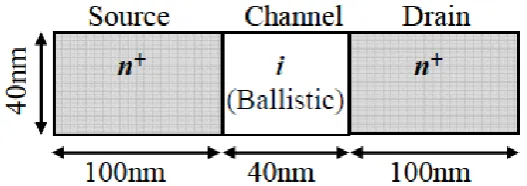
Figure 1: Schematic of structure of silicon ballistic channel n+-i-n+ diode.
Numerical Analysis Method
10 for intravalley acoustic phonon scattering. The electron concentration profile is calculated by the cloud-in-cell method and the potential profile is calculated by the finite difference method scheme of the Poisson equation.[8] The steady-state current is computed using the Ramo-Shockley formula.[11,12] The channel region is assumed to be intrinsic and ballistic. Electrons do not suffer any scattering throughout the channel. The different cases of scattering are studied in the drain region.
Case A: The drain region is ballistic. Electrons do not suffer any scattering throughout the drain.
Case B: Only intravalley acoustic phonon scattering is considered in the drain region.
Case C: Intravalley acoustic phonon and ionized impurity scatterings are considered in the drain region.
Case D: Intravalley acoustic and intervalley phonon scatterings are considered in the drain region.
Case E: Intravalley acoustic, intervalley phonon, and ionized impurity scatterings are considered in the drain region.
Intravalley acoustic, intervalley phonon, and ionized impurity scatterings are considered in the source region for all cases. Intravalley acoustic phonon scattering can be considered as an elastic scattering owing to the fact that the acoustic phonon energy is much lower than kBTat
room temperature, where kBis the Boltzmann constant and Tis the lattice temperature.
The intervalley phonon energy is comparable to the average thermal energy of carriers at room temperature and the intervalley phonon scattering is therefore regarded as inelastic. Ionized impurity scattering is treated as an elastic process. The doping concentrations of the source/drain are set to be ND = 1018 and 1020 cm-3,respectively. The scattering rate of
ionized impurity scattering is computed by the Brooks-Herring approach[8] when ND = 1018
cm-3 and using Kosina’s model[13, 14] when ND= 1020 cm-3. Kosina’s model has been shown
to be adequate for doping concentrations up to 1020 cm−3.
RESULTS AND DISCUSSION
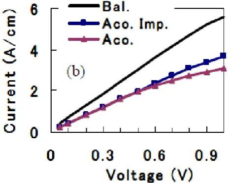
the current-voltage characteristics of a ballistic n+-i-n+ diode for cases A, B, and C with ND = 1018 cm-3.For all cases, the mean velocity of electrons is decreased in the drain region, because there are many “cold” electrons with low velocity in the drain region.
When the drain region is ballistic (case A), all hot electrons are absorbed in the drain region and are not transported in the backward direction since scattering does not occur. Therefore, case A has the largest peak of the mean velocity of electrons in the channel as well as the largest steady-state current. When only the intravalley acoustic phonon scattering is considered in the drain region (case B), results are in accordance with the theory of elastic/inelastic scattering as described by Kurusu and Natori.[6]
Figure 2 (a) Distribution of mean velocity of electrons along X-axis at VD= 0.3 V, and (b)
I-VD characteristics of ballistic channel n+-i-n+ diode, for cases in which the drain region
is ballistic (case A, solid line), only acoustic phonon scattering is considered (case B, triangles line) and both of acoustic phonon and ionized impurity scatterings are considered (case C, squaresline). Here, the doping concentration of source/drain is ND =
1018 cm-3.
Figure 3: (a) Distribution of mean velocity of all electrons along X-axis at VD= 0.3 V, ND
= 1018 cm-3 and (b) I-VD characteristics of ballistic n+-i-n+ diode, for cases in which the
drain region is ballistic (case A, solid line), intravalley acoustic and intervalley phonon scatterings are considered (case D, squares line) and intravalley acoustic, intervalley phonon, and ionized impurity scatterings are considered (case E, triangles line). Here, the doping concentration of source/drain is ND = 1018 cm-3.
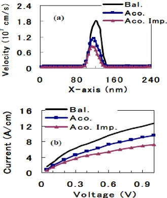
Figure .4 (a) Distribution of mean velocity of all electrons along X-axis at VD = 0.3 V and
(b) I-VD characteristics of ballistic n+-i-n+ diode, for case A (solid line), case B (squares
line) and case C (triangles line) with ND = 1020cm-3.
of ionized impurity scattering leads to a minor change in the peak of the mean velocity of electrons in the channel and the steady-state current. It must be mentioned that ionized impurity scattering approaches the isotropic state and obviously increases the rebound of hot electrons in the backward direction at sufficiently high doping concentrations. These effects will severely degrade the peak of the mean velocity of electrons in the channel and the steady-state current.
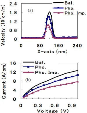
Figure 5 (a) Distribution of mean velocity of all electrons along X-axis at VD = 0.3 V and
(b) I-VD characteristics of ballistic n+-i-n+ diode, for case A (solid line), case D (squares
line) and case E (triangles line) with ND= 1020 cm-3.
ionized impurity scattering is considered in the drain region when the doping concentration is
ND=1020 cm-3.
CONCLUDING REMARKS
Intravalley acoustic phonon scattering within drain severely degrades peak of the mean velocity of electrons in the channel and the steady-state current of the device,because the scattering substantially increases the backward flow of hot electrons. The reason is that the intravalley acoustic phonon scattering is not only an elastic scattering,but is an isotropic scattering and has a random scattering direction. At low doping concentrations, the ionized impurity scattering has a weak influence on hot electron transport because of its anisotropic characteristics with a high probability for forward-scattering events. On the other hand, the scattering assumes an isotropic character at sufficiently high doping concentrations, and increases the scattering of hot electrons in the backward direction, severely degrading the peak of the mean velocity of electrons in the channel and also the steady-state current. It is concluded that the scattering direction is an important factor for the hot electron transport within drain of semiconductor devices. Both the peak of the mean velocity of electrons in the channel and the steady-state current are decreased if the rebound of hot electrons in backward direction is increased in the drain region.
REFERENCES
1. ITRS 2011 [http://www.itrs.net/].
2. K. Natori, “Scaling Limit of the MOS Transistor-A Ballistic MOSFE”, IEICE Trans. Electron., 2001; E84-C: 1029.
3. P. Palestri, D. Esseni, S. Eminente, C. Fiegna, E. Sangiorgi, and L. Slemi, “AMonte-Carlo study of the role of scattering in deca-nanometer MOSFETs”, IEDMTech. Dig., 2004; 605.
4. M. Fischetti, and S. Laux, “Monte Carlo study of sub-band-gap impact ionization insmall silicon field-effect transistors”, IEDM Tech. Dig., 1995; 305.
5. A. Svizhenko, and M. P. Anantram, “Role of scattering in nanotransistors”, IEEETrans. Electron Devices., 2003; 50: 1459.
7. T. Gonzalez, and D. Pardo, “Physical models of ohmic contact for Monte Carlo device simulation”, Solid-State Electron., 1996; 39: 555.
8. K. Tomizawa, Numerical simulation of submicron semiconductor devices. (Artech House, 1993).
9. C. Jacoboni and L. Reggiani, “The Monte Carlo method for the solution of chargetransport in semiconductors with applications to covalent materials”, Rev. Mod. Phys., 1983; 55(3): 645.
10.G. Donnarumma, J. Wozny, and Z. Lisik, “Monte Carlo simulation of bulksemiconductors for accurate calculation of drift velocity as a parameter fordrift-diffusion, hydrodynamic models”, Mater. Sci. Eng. B., 2009; 165: 47.
11.W. Shockley, “Currents to Conductors Induced by a Moving Point Charge”, J. Appl. Phys., 1938; 9: 635.
12.S. Ramo, “Currents Induced by Electron Motion”, Proc. IRE., 1939; 27: 584.
13.H. Kosina, “A method to reduce small-angle scattering in Monte Carlo device analysis”, Transaction on Electron Devices., 1999; 46: 1196.