FPGA Implementation of Baseband
Modulation for Transceiver of 802.16e
(Wi-MAX)
Abhishek Agrahari*
MTech (Research) Scholar
Electronic & Communication Engineering Department Sardar Vallabhbhai National Institute of Technology (NIT Surat)
Surat- 395007, Gujarat www.svnit.ac.in
Anand Darji
Assistant Professor,
Electronic & Communication Engineering Department Sardar Vallabhbhai National Institute of Technology(NIT Surat)
Surat -395007 Gujarat www.svnit.ac.in
Abstract –
In this paper, we have presented the hardware implementation of Convolutional Encoder and Viterbi Decoder for an OFDM based wireless MAN standard, viz. IEEE 802.16e, popularly known as Mobile WiMAX [4]. WiMAX networks specify data rates above 100 Mbps. For the selected design parameters of code rate = ½ and constraint length = 3, we have obtained a data rate as high as 211 Mbps on implementing our design on Xilinx Spartan 3e FPGA. Here, we describe briefly the Viterbi algorithm, our design methodology of implementing it in VHDL and final implementation results using Xilinx ISE software. Finally, error performance plots were obtained on MATLAB, which bear a close match with theoretical results.
Keywords – WiMAX, Convolutional Encoder, Viterbi Decoder, Maximum likelihood decoding, data rate, hamming distance, Spartan FPGA
INTRODUCTION
Viterbi algorithm is widely used in channel decoders for satellite and other noisy communication channels. It basically implements maximum likelihood decoding rule, which states that the path traced in the trellis with minimum hamming distance must the most likely path to contain the original data sequence. The convolutional encoded data contains redundant information which is used to implement forward error correction techniques which are now the most widely used in digital communication systems. The encoded data is transmitted after being multiplexed, which further boosts up the data rate, and modulated using PSK or QAM. The decoder receives the message after demultiplexing and demodulation are performed at the front end of the receiver. The decoder employing Viterbi algorithm retrieves the original data bits from encoded code words. Thus, the Viterbi decoder is optimum in combating the channel errors due to noise and intersymbol interference.
Our FPGA based project is aimed at providing a better bit error rate immunity and improvement in speed for WiMAX. In section II, we first briefly describe the algorithms of convolutional encoder and hard decision Viterbi decoder. We have considered a binary symmetric channel for our implementation. In section III, we discuss at length the hardware implementation flow of our design using selected design parameters of code rate = ½ and constraint length = 3. The coding for encoder and decoder was done on a VHDL platform in an Xilinx Integrated Simulation Environment (ISE) tool. In section IV, the results and conclusion of our project work are described.
ALGORITHM
fixed length n for each of the k length input bits. The Constraint length of the convolutional encoder [2] determines the number of shifts over which the message bits are to be shifted to form a linear convolution of data sequence with the impulse response of the encoder.
Viterbi algorithm implements maximum likelihood decoding procedure. Basically, it implements Maximum Likelihood Decoding Procedure Rule, which Says that “For N-dimensional signal space, choose a signal vector that is closest in Euclidean distance to the received vector, to achieve minimum probability of error ( PE) for given EB/N0 ratio.”
There are several decoding methods based on this algorithm: namely register exchange method and the traceback method. The concept is to find out a sequence in the trellis diagram which has a minimum hamming distance. This path will definitely contain minimum errors and will be closest to the correct data sequence.
HARDWARE IMPLEMENTATION
The parameters chosen in our design are as follows:
1.Constraint Length: K=3: That is the number of shifts (i.e. flip flops) in the linear shift register over which the input data bits have to be shifted before they are taken out of the shift register.
2.Code Rate: k/n = ½: That is for every input message bit, there are two output bits created out of convolution of the impulse response of the linear shift register and the input bit sequence.
3. Minimum Free Distance = 5: That is the minimum Hamming Distance between the codeword sequence and the all zeroes codeword sequence.
4. Trace Back Depth=15: That is the number of paths in Trellis Diagram or the branches in the Tree Diagram, which must be covered before the first input bit can be decoded.
Now we describe the three basic entities used in our VHDL design.
A. Convolutional Encoder Model:
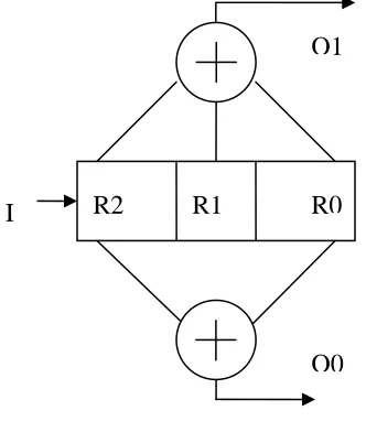
Fig. 1 Structure of Convolutional Encoder
As shown in fig. 1, it uses a linear feedback shift register of 3 D flip-flops & 2 XOR Gates acting as function generators.
XOR1 = S2 xor S0 and XOR2 = S2 xor S1 xor S0
B. Binary Symmetric Channel Model:
Channel Output suffers an error due to channel noise, so it is given as - Encoder Output XOR Noise
I
R2
R1
R0
O0
O1
C. Viterbi Decoder Model:
The complete hardware model of our design is shown in fig 2. Here we consider the different units of this model [6].
1. Branch Metrics Unit:
It calculates branch metrics for each of the 2-bit code sequences. For K=3, a total of 8 branches corresponding to 4 states, each of which has a corresponding 2-bit hamming distance stored in a 16-bit register.
2. Add Compare Select Units:
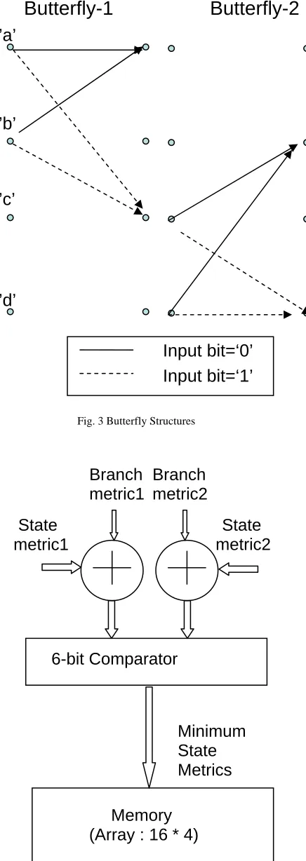
The next state metrics of a given state is defined as the sum of previous state metric of the state corresponding to the incoming surviving path plus the hamming distance along that path. The algorithm requires two Butterfly Structures shown below whose hardware implementation is shown in fig. 3. Two 6-bit adders add one 6-bit state metric and one 2-bit branch metric. These two values are computed and then compared in the comparator unit. Then the minimum of the two values is stored in the memory. Also stored in the memory is one path history bit which is computed in Path History Unit, so the optimum organization of Path History Block is 16 * 4. Only because it is going to generate, that is decode, the input message bit.
Fig 2. Viterbi Decoder Model
Clock Reset
Controller
Channel Output bit
pairs BMU
In Built Memory
ACS UNIT
Memory storing State Metrics and
PHR array Trace Back Block
Fig. 4 Add Compare Select Unit
State
metric1
Branch
metric1
Branch
metric2
State
metric2
6-bit Comparator
Minimum
State
Metrics
Memory
(Array : 16 * 4)
’a’
’b’
’c’
’d’
Input bit=‘0’
Input bit=‘1’
Butterfly-2
Butterfly-1
Fig. 3 Butterfly Structures
Path History Unit:
Whenever each state metrics is computed and stored in memory, 1-bit for path memory is also stored in memory, indicating what path enters a given state from the previous 2 possible states The Organization of the Path History Block is as follows: As there are 4 states at any time in the encoder, and the Traceback Back Depth required is a minimum of 15 for the chosen parameters for optimum Bit Error Performance, so the optimum organization of Path History Block is 16 * 4, that is 16 4-bit registers that is a total of 64 flip-flops for this block. If the surviving path coming to a given state comes from a lower state, the corresponding will be ‘1’, else ‘0’.
Traceback Unit:
This unit works only after the depth covered in the Trellis Diagram is 15, hence at the 16th clock cycle, the first input message bit is decoded and is output from the Viterbi Decoder [5]. The unit performs traceback over the path with minimum metric to get the correct data bit sequence.
Control Unit:
This unit governs the processing operations of the different units of the Viterbi Decoder. On hardware there is a multiplexer that determines the different operations on each event of clock.
Also, that when the encoder reaches steady state, the amount of processing load and the memory required will be different. This is also handled by this counter.
We have used Xilinx ISE software to implement the design on Spartan-2 and Spartan 3e FPGAs. These are the most advanced FPGAs in the Spartan Family with abundant logic, memory and routing resources.
Fig. 5 FPGA Design Flow
Behavioral and timing Simulation are performed after writing a separate test bench for each separate entity. Then, after the synthesized netlist produce a RTL schematic. The design is then implemented using Xilinx Impact Tool. FPGA implementation involves Translate, Mapping and Place and Route. Here the logic , memory and routing resources available on the FPGA are assigned to the different circuits required for implementation of our design that has been synthesized using Xilinx Synthesis Technology tool. Finally, a programming file is generated which is downloaded on the FPGA.Because the SRAM devices lose their configuration when power is turned off, the bitstream is stored in a serial PROM. There is an associated hardware that connects from the computer to a board containing the target device.
RESULTS
We present the results of synthesizing our design using Xilinx Synthesis Technology Tool on Xilinx Spartan XC2S200-5PQ208 FPGA and Xilinx Spartan XC3S500E-FGG320 FPGA.
As shown in the Table 1, the different circuits used on the two FPGAs are mentioned. As we see, the number of different circuits used in the designs is same.
Design Specification
Design Entry in HDL
Synthesis Using Xilinx Synthesis
Technology
Functional Simulation
Implementation
Translate
Place & Route
Download
Test Vectors
Timing Simulation
Table 1 Circuits Synthesis Results
The following table 2 lists the number of resources utilized on the two FPGAs.
Device Utilization Summary
Resources Spartan 2 FPGA Spartan 3E FPGA Number of Slices 952 (40% ) 922 (19%) Number of Slice Flip
Flops
410 (8% ) 402 (4%) Number of 4 input
LUTs:
1855 (39%) 1811 (19%) Number of IOs 4 4
Number of GCLKs: 2 (50%) 2 (8%) Table 2 Device Utilization Summary
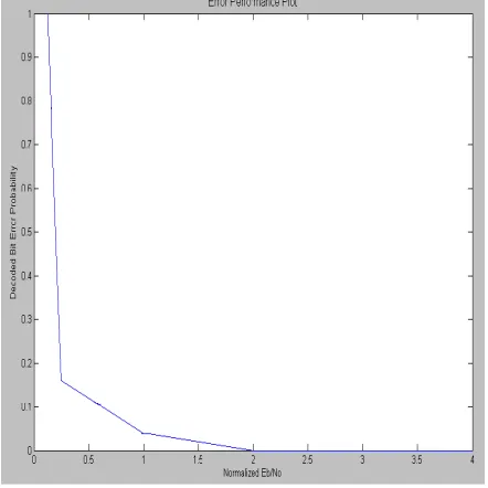
The implemented design on Spartan 2 FPGA can operate at 37 MHz, while the more advanced FPGA, i.e. Spartan 3e, with more logic and routing resources can run our design at a maximum frequency of 211 MHz. The equation for Bit-Energy Eb is given as product of Voltage level of data bits and time period of data bits. For this plot, the ratio
of time period divided by noise power spectral density has been normalized to unity, when the bit period is in microseconds. Our simulation results reveal that the decoder corrects up to atleast 5 continuous errors bits in a sequence of 25 bits, which clearly satisfies minimum error correcting capability of the code.
Figure 6 [Practical Plot] Decoded Bit Error Probability versus Normalized Eb/No for constraint length K = 3 with
Hard Decision Viterbi Decoding
Circuits Number of Instances Utilized on Spartan 2 & Spartan 3E FPGA
6-bit adder 109
5-bit up counter 1 7-bit up counter 1
Flip-Flops 423 6-bit comparator less 6
As shown in the above figure 6, for a data rates less than 500 Kbps, we get nearly zero Bit Error Probability and for data rates above and equal to 8 Mbps, the Bit Error Probability is nearly unity. The attained speed is limited by instruments available at the VLSI laboratory of our institute.
V. CONCLUSION
We have completed the design of Convolutional Encoder and Viterbi Decoder for code rate = ½, that achieves minimum decoding delay, data rate upto 211 Mbps at the optimum Constraint Length K = 3, with hard decision decoding and reasonable hardware complexity
REFERENCES
[1] B. Sklar, Digital Communications, Fundamentals and Applications, Second Edition, New Delhi, Pearson Education, 2004. [2] Convolutional Codes and ’Their Performance in Communication Systems ANDREW J. VITERBI, SENIOR MEMBER, IEEE [3] Xilinx, Xilinx Synthesis and Simulation DesignGuide, 2002
[4] Mobile WiMAX, A technical Overview and Performance Evaluation, prepared on behalf of WiMAX Forum, 2006.
[5] J.A. Heller and I. M. Jacobs, “Viterbi Decoding for Satellite and Space Communications”, IEEE Trans. Commun. Technol., vol. COM19, no. 5, 1971.
[6] Viterbi Decoding in Field Programmable Gate Arrays, Chameleon Logics, downloaded in March 2008. [7] Xilinx, Spartan 3E Starter Kit Board User Guide UG230 (v 1.0), 2006.