Volume 13, Issue 7 (July 2017), PP.06-12
Design of Synthesizable Asynchronous FIFO And
Implementation on FPGA
Hemant Kaushal
1, Tushar Puri
21
Student, School Of Electronics, M.Techvlsi(2015-17),CDAC–Noida, [email protected]
2
Student, School Of Electronics, M.Tech VLSI (2015-17), CDAC–Noida, [email protected]
ABSTRACT:
This paper presents a design of asynchronous FIFO which, along with the regular status signals,consists of some extra status signals for more user-friendly design and added safety. Gray code pointers are used in the design. For synchronisation purpose, two synchroniser modules are used which contain two D-flip-flops each. The design is implemented and synthesised at register transfer level (RTL) using Verilog HDL. Simulation and implementation is done using Xilinx ISE Design Suite. Further, the design is implemented on Basys 2 Spartan-3E FPGA Board. Asynchronous FIFO is used to carry out steady data transmission at high speeds between two asynchronous clock domains.
Keywords:
Asynchronous FIFO; FPGA; Verilog HDL.I.
INTRODUCTION
Asynchronous FIFO is a design in which the data is written into the FIFO memory in one clock domain and is read from the same memory in another clock domain. The two clock domains are asynchronous to each other. Asynchronous FIFO is used in asynchronous communication where write and read speeds are different. Hence, by using them we can safely pass data from one clock domain to the other clock domain. The main problem which arises here is the generation of FIFO pointers (read pointer and write pointer) and comparing them to find FIFO full and empty conditions. The write pointer points to the next location to be written into the memory and read pointer points to the current location to be read from the memory. They both are set to zero on reset. The generation of FIFO pointers is of utmost importance because they are clocked at different clocks so they need to be synchronised if they are used in other clock domain. These synchronised pointers are then compared to generate full and empty conditions.
Empty condition arises when read pointer and write pointer both are equal. This condition can happen when both pointers are reset to zero or when read pointer catches up the write pointer i.e. the last word from the FIFO has been read. Full condition arises when the pointers are again equal but this time write pointer catches up the read pointer i.e. the last location of the FIFO memory has been written. To distinguish between these two conditions, one extra bit is added to each pointer. Thus, if all the bits except MSBs of both the pointers are equal then FIFO is full. Also, if all the bits including MSBs of both the pointers are equal then FIFO is empty. For a FIFO with 2(n-1) writable locations, n-bit pointers are used where (n-1) bits are required to address the FIFO memory. To generate FIFO full and empty conditions, the two pointers are compared in different clock domains i.e. read pointer should be synchronised with the write clock domain to be compared with the write pointer and vice-versa. Gray coded values are used instead of binary values for the pointers because every single bit can change simultaneously in the case of binary pointers, thus synchronising binary values is problematic. Gray codes allow only one bit to change for each clock transition, eliminating the problem of synchronising multiple bits at a time.
The paper is organised as follows: Section II describes the architecture of asynchronous FIFO and explains each of its module in detail. Section III describes Simulation Results which include simulated waveforms, RTL schematic of asynchronous FIFO, timing report and design utilisation summary. Section IV presents realisation of the design on FPGA.
II.
MODULE DESCRIPTION
In this section, all the modules in the design are explained one by one. Verilog HDL is used to code the design. The tool used for simulation and implementation of the design is Xilinx ISE Design Suite with ISim as simulator
A.FIFO_top
It is the top module of the design. All other constituting modules are instantiated inside this module. This module can be instantiated inside the system that will use the FIFO. This top module is synthesized, implemented and then converted into the bit file required for implementation of the design on FPGA. This bit file is then dumped on the FPGA. Write clock (wr_clk) domain signals include 3 input signals, which are data_in, wr_rstn and wenable, and 3 output signals, which are full, near_full and overflow. Read clock (rd_clk) domain signals include 3 input signals, which are data_out, rd_rstn and renable, and 3 output signals, which are empty, near_empty and underflow.At positive edge of wr_clk, data_in is latched onto FIFO memory if wenable is high. And at positive edge of rd_clk, data_out is taken out from FIFO memory if renable is high. wr_rstn and rd_rstn signals are used to reset the FIFO.
Figure 1: Top module FIFO_top
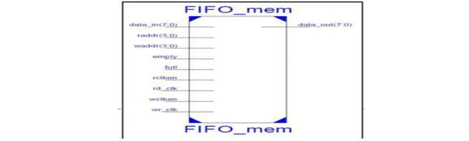
B. FIFO_mem
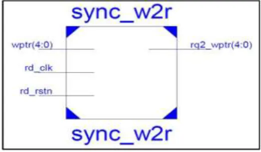
C. sync_r2w
This is the synchroniser module that is used to synchronise the read pointer to write clock domain. As shown in figure 4, sync_r2w (also sync_w2r) contains two D-Flip-flops for its working. The two flip-flops are clocked by the destination clock.
Figure 3: Synchroniser module sync_r2w
Figure 4: Two D-FFs in synchroniser module
D. sync_w2r
This is the synchroniser module that is used to synchronise the write pointer to read clock domain.
E. rptr_empty
This module is synchronous to read clock domain and contains logic for empty, near_empty and underflow. Near_empty (also near_full) is also made parameterised. This module also contains binary to gray code converter which converts binary read pointer to its gray code equivalent. By doing this, FIFO is made reconfigurable at run-time and we can change this value as per the need.
Figure 6: Module containing empty, near_empty and underflow logic
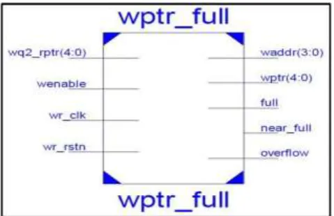
F.wptr_full
This module is synchronous to write clock domain and contains logic for full, near_full and overflow. This module also contains binary to gray code converter which converts binary write pointer to its gray code equivalent.
Figure 7: Module containing full, near_full and verflow logic
III. SIMULATION RESULTS
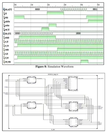
Figure 8: Simulation Waveform
Figure 9: RTL schematic of Asynchronous FIFO
The timing report is also extracted which gives timing details (at Speed Grade -4). The minimum period of the design turns out to be 6.809 ns i.e. maximum frequency is 146.864 MHz.
Figure 11: Timing report summary
IV. FPGA REALISATION
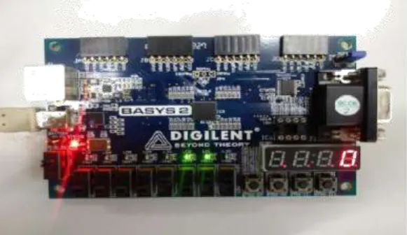
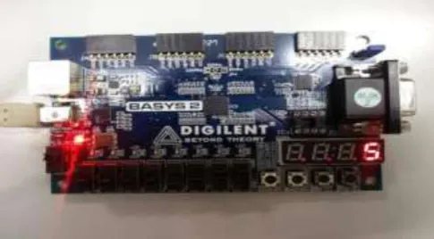
The bit file generated by implementing the asynchronous FIFO design is downloaded onto FPGA. The FPGA used is Basys 2 Spartan-3E FPGA Board. It is used in the configuration xc3s100e-4cp132. For implementing the design on Spartan 3E FPGA, we take some data inputs from a predefined memory. These data inputs are saved in this memory and from there they are given to the FIFO memory (FIFO_mem) as „data_in‟The write and read clocks are downgraded to 1 second and 2 second respectively by applying counters to the main clock. This is done to show the „data_out‟ on the seven segment display. The 20ns (50 MHz) clock will not be able to do the same. The output will not be seen with the naked eye if 20ns clock is used. Also the output LEDs will turn on in no time if 20ns clock is used. So, to illustrate the working of the FIFO on FPGA, downgrading of the clocks is done. The „data_out‟ is also shown on seven segment display. Some scenarios are shown in figure 11, figure 12 and figure 13.„renable‟, „rd_rstn‟, „wenable‟ and „wr_rstn‟ are implemented on slide switches. „empty‟, „near_empty‟, „underflow‟, „full‟, „near_full‟ and „overflow‟ are implemented on LEDs
Figure 13: „wenable=1‟ when „full=1‟ condition is reached, results in „overflow=1‟
Figure 14:‟seven segment display‟ showing „data_out‟ from the FIFO.
V.
CONCLUSION
The asynchronous FIFO is successfully implemented on FPGA. The FIFO is made parameterised and also additional status flags like „underflow‟, „overflow‟, „near_empty‟ and „near_full‟ are included in the design to make the design safer. The design turns out to be of high speed with maximum frequency146.864 MHz.
REFERENCES
Shruti Sharma, “Implementation of an RTL synthesizable asynchronous FIFO for conveying data by avoiding actual data movement via FIFO”
[2]. proposed in Computing, Communication and Networking Technologies (ICCCNT), 2015 6th IEEE International Conference on 13-15 July 2015.
Xinrui Zhang, Jian Wang, Yuan Wang, Dan Chen, Jinmei Lai, “BRAM-based Asysnchronous FIFO in FPGA with Optimized Cycle Latency” proposed in Solid-State and
[4]. Integrated Circuit Technology (ICSICT), 2012 IEEE 11th International Conference on 29 Oct-1 Nov 2012.
Yanjun Zhang, Chunli Yi and Jinqi
[6]. Wang, “Asynchronous FIFO Implementation Using FPGA”,
[7]. International Conference on Electronics and Optoelectronics, IEEE Conference Publications, 2011, Volume 3.
HaythamAshour, “Design, Simulation and Realisation of a parameterizable,