112 | P a g e
CONTINUOUS CONTROLLER DESIGN FOR THE
BOOST CONVERTER VIA PSIM
Dr. P.S.Jagadeesh Kumar
1, Prashant Thapliyal
2Electrical Engineering Department, DIT University, Dehradun U.K. (India)
ABSTRACT
This paper represents the simulation modeling of DC-DC convertor (boost convertor) in practice there are so many design techniques available such as direct digital control, digital redesign etc. Before moving to implement such techniques we require to design our controller in continuous s- domain in order to get complete view about the parameter variation in time domain. Since converter dynamics is very important to study before the development of real-time systems. PSIM (power electronics, motor drives, and dynamic system simulation) simulation software specifically designed for power electronics simulations is a tool designed for studying the converter dynamics in an easier manner.
Keywords: PSIM, Boost converter, Bode plot, Controller, Root locus, MATLAB (Simulink)
I. INTRODUCTION
In power electronics Boost converter is the basic topology under DC–DC converter, whose behavior serves to
convert a DC input voltage to a Higher DC output voltage, which has been widely used in engineering. It is an important step for designing of a Boost converter is to model and analyze this converter according to the real
requirements [1].For implementation of the real converter an engineer needs to possess the system behavior and its
dynamics. Controller design is an added advantage in practice if we want that system should respond according to
our needs. It involves tedious mathematics to solve various integro-differential equations. As a matter of fact
semiconductor devices involved in the system brings non-linearity which further increases the work of calculations.
To have an insight with prior knowledge boost converter operates in two modes:
Continuous Conduction Mode (CCM).
Discontinuous Conduction Mode (DCM).
So as assumed here CCM is easy approach for studying DC-DC converters and can better deliver the insight related
113 | P a g e
II. Boost Converter
The overall objective associated to converter simulation is wholly dependent on the system circuit model. There are
two states associated with a boost converter:
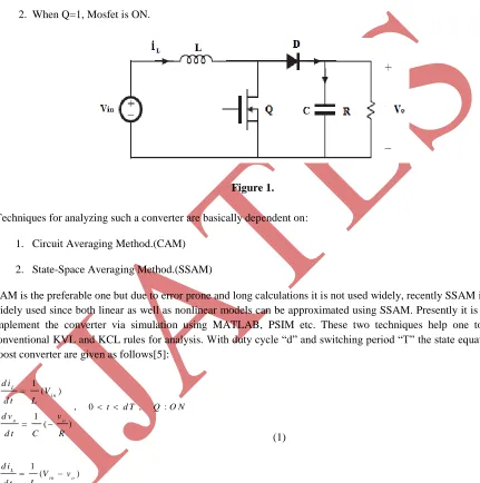
1. When Q=0, Mosfet is OFF.
2. When Q=1, Mosfet is ON.
Figure 1.
Techniques for analyzing such a converter are basically dependent on:
1. Circuit Averaging Method.(CAM)
2. State-Space Averaging Method.(SSAM)
CAM is the preferable one but due to error prone and long calculations it is not used widely, recently SSAM is being widely used since both linear as well as nonlinear models can be approximated using SSAM. Presently it is easy to implement the converter via simulation using MATLAB, PSIM etc. These two techniques help one to apply conventional KVL and KCL rules for analysis. With duty cycle “d” and switching period “T” the state equations of boost converter are given as follows[5]:
1 ( )
, 0 , :
1 ( ) L i n o o d i V d t L
t d T Q O N
d v v
d t C R
(1)
1 ( ) , , : 1 ( ) L
i n o
o o
L d i
V v d t L
d T t T Q O F F
d v v
i d t C R
(2)
III. CONTROLLER DESIGN METHODS
114 | P a g e
1. Transfer Function Based Controller Design Methods (TFBCD): System modeled here is Linear timeinvariant (LTI) as well as Single-input and Single-output (SISO).
2. State Space Controller Design Methods (SSCD): System modeled here is Multiple-input and multiple-output system (MIMO).
The adopted method to design controller is TFBCD since assuming system to be LTI and SISO therefore classical techniques available are as:
Root locus.
Bode diagram.
Nyquist Diagram.
Inverse Polar plot.
Nicholas chart.
The classical methods above are well suited methods but root locus is enough for predicting the results for lower order as well as higher order systems, Bode diagram is also popular technique among designers but it fails for the non-minimum phase systems.
IV. STATE SPACE MODELLING OF BOOST CONVERTER USING MATLAB
clear all;
clc
Vg=15;%input volatge D= 0.4;%Duty ratio L= 2e-3;%Inductance C= 10e-6;%capacitance R= 100;%load resistance
As= [0 -(1-D)/L ;(1-D)/C -1/(R*C)]; Bs= [1/L 0 0; 0 -1/C 0];
Cs= [0 1; 1 0]; Ds= [0 0 0];
Vo= -Cs(1,:)* inv(As)*Bs(:,1)*Vg Ig= -Cs(2,:)* inv(As)*Bs(:,1)*Vg
a=[0 -(1-D)/L;(1-D)/C -1/(R*C)]; b=[1/L 0 Vo/L;0 -1/C -Ig/C]; c=[0 1];
d=[0 0 0];
ulabels= ['vg iz d'];
ylabels=['vo ig'];
xlabels=['il vc'];
115 | P a g e
-1 0 1 2 3 4 5 6 7
x 104 -2
-1.5 -1 -0.5 0 0.5 1 1.5
2x 10
4
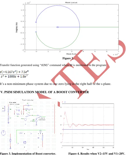
Root Locus
Real A xis
Im
ag
in
ar
y
Ax
is
Figure 2.
Transfer function generated using “tf(M)” command where M is mentioned in the program:
It’s a non-minimum phase system due to one zero lying in the right half of the s-plane.
V. PSIM SIMULATION MODEL OF A BOOST CONVERTER
Figure 3. Implementation of Boost converter. Figure 4. Results when V2=15V and V1=20V.
Parameters are chosen for implementation as shown in M-file are as follows Vg=15;(input voltage)
;
L= 2e-3;(Inductance);
C= 10e-6;(capacitance);
R= 100;(load resistance).116 | P a g e
Figure 5.Example for buck converter design type-3 compensation Network[13].REFERENCE
[1] Kazimierczuk M K , “Pulse-width Modulated DC–DC power converters” (London: John Wiley and Sons, 2008).
[2] Young-Joo Lee and Ali Emadi , “Phase Shift Switching Scheme for DC/DC Boost Converter with Switches in Parallel”, IEEE Vehicle.
[3] Power and Propulsion Conference (VPPC), September 3-5, 2008, Harbin, China.
[4] Omar Hegazy, Joeri Van Mierlo and Philippe Lataire,“Analysis, Control and Comparison of DC/DC Boost Converter Topologies for Fuel Cell Hybrid Electric Vehicle Applications”.
[5] Alan Martin, Boost Converter Design Tips, in Field Applications Engineering, National semiconductors, March 2005.
[6] R. Krishnan, Electric Motor Drives- Modeling, Analysis and Control, 10th edn.,Prentice Hall, Upper Saddle River, NJ, 2001.
[7] Alan Martin, “Boost Converter Design Tips, in Field Applications Engineering”, National semiconductors, March 2005.
[8] Muhammad H. Rashid, Power Electronics- Ciruits, Devices, and Applications, 9th edn.,Springer-Verlag, New York, 2011.
[9] Magnus Hedlund, “Design and Construction of Bidirectional DC-DC Converter for an EV Application”, (http://www.teknat.uu.se/student, Feb, 2010).
[10] Bryant, B. Kazimierczuk, M.K., “Small-signal duty cycle to inductor current transfer function for boost PWM DC-DC converter in continuous conduction mode”, Proceedings of the International Symposium on Circuits and Systems, ISCAS '04, 23-26 May 2004,Vol. 5, pp: 856-859.
[11] Mehrdad Ehsani, Yimin Gao, and Ali Emadi ,” Modern Electric, Modern Hybrid, and Fuel Cell Vehicles”,Book, 2010 by Taylor and Francis Group, LLC.
[12] Doug Mattingly, “Designing Stable Compensation Networks for Single Phase Voltage Mode Buck Regulators”, Intersil, Technical Brief Dec-2003.