959
Efficient Configurable Crossbar Switch Design For
Noc
Vivek tiwari, Kavita khare
Abstract :Network-on-Chip is an emerging paradigm for integrating very high number of Intellectual Property blocks on a single Integrated Chip. Crossbar switch is one of the important parts of NoC. In this paper, 2x1 MUX are used instead of existing crossbar design with 4x1 MUX, to meet the requirement of high speed networks. The proposed design reduces area by 40% and delay by 7.14 % as compared to 2-D cross bar switch as well as conventional crossbar switch. The functional verification and synthesis of proposed cross bar switch design is done by using Xilinx ISE 9.2i
Keywords: Network-on-Chip; NoC router; crossbar switch; Xilinx; RTL simulation, MUX;
————————————————————
I.INTRODUCTION
Device sizes are continuously reducing as a result of advancement in process technology. Due to this multiple processing elements (PEs) can be integrated into a single a chip, referred as system-on-chip (SoC). SoC technology offers many advantages over conventional approach such as higher performance and low power consumption. But in SoC due to large number of PEs, communication between cores becomes very complicated. In some SoC system where communication links is much larger than the number of PEs multiple communication links may require and it can make these communication networks very complex. In conventional on-chip communication architecture, it consists of bus-based infrastructure and point-to-point communication network, may not be able to provide adequate communication support for SoC. Generally bus–based infrastructure and point-to-point communication network is used in conventional on-chip communication architecture, as number of cores is increasing continuously over SoC, so communication infrastructures is not efficient. To provide better communication between cores of SoC Network-on-chip architecture is a better solution now-a-days[1].
(a) (b) (c)
Fig.1 Connection between different cores of multiprocessor (a) Point to point connection (b) Bus based connection (c) Network based connection [30].
Fig.1 (a) shows point to point connection between two modules through direct link assign to them. In this type connection large number of link will required which will increase size of chip. Because of long communication wire there is excessive signal delay. Fig.1 (b) shows bus based communication network which is efficient and flexible compare to point to point communication. In bus based communication the whole communication network is utilized only by two modules at a time because of this all module become idle in this time. Thus the bus may become a bottleneck of overall system performance where heavy communication is required. Fig.1(c) show a packet switched networking infrastructure based solution that can be a promising solution for above discussed problem. This type of approach for communication between nodes referred to as network-on-chip (NoC)[2–5][30]. In NoC, router is used to transferred data in packed switched network, package of data can be further divided into multiple flow information units (flits) that are actually transmitted. NoC greatly improves the scalability of SoCs and achieves higher power efficiency compared to other types of communication structures. As compare to other types of communication structure, NoC provide great improvement in scalability of SoC. it also provide higher efficiency in term of area, delay and area [25]. In NoC based communication system different cores such as processors, memories application specific integrated circuits and intellectual properties exchange their data through the NoC, which consists of router, data links and network interfaces Data links are used to transmit data over communication media and NI provide interface between PE and a router, where it is Responsible to transforming data into packet and vice versa. Physical path for data transmission is decided by routers [28].
_____________________
960
Fig.2 5x5 NoC Router architecture [25]
A 5x5 NoC router architecture shown in Fig.2, consisting of input port, output port, input buffer, arbiter and crossbar switch. In this NoC router it is shown that a 5x5 crossbar switch is used to connect 5 input channels to 5 output channels [7, 31]. In this paper new efficient crossbar switch architecture is proposed, which also consists five input ports and five output ports. This crossbar switch provides connection between north ports to south port, east port to west port and simultaneously, which is main feature of our proposed work. It also provides connection between all the four ports (i.e. east port, west port, north port, south port) to local port same as conventional crossbar switch. This proposed design is simulated in Xilinx 9.3 and its result i.e. RTL view, simulation, area, power delay is compared with 2-D crossbar switch and conventional crossbar switch [6]. In this proposed efficient crossbar switch area and delay significantly reduces [6]. And it is also proposed that when this crossbar switch is implemented within NoC router, it will become Faster and more efficient [26].
II-Related Work
In NoC we use a Crossbar switch to connect input port to output port which is a collection of switches arranged in the form of matrix configuration [8]. It has multiple input and output lines arranged in the form of row and column. Input-Output lines get arranged in such a way that they cross each other and a switch is placed between them, by closing these switch connection could be established. When switches at interconnection are closed connectivity is established between one of the input to output. Crossbar switch is a non-blocking type switch i.e. it does not affect any other concurrent input, output connection. In any NoC, crossbar switch and input- output buffer is main power and area contributor [9-15]. Decomposition and segmentation method are previously used for reduction of area and power [10,11,16-22]. In decomposition method, the larger crossbar switch is decomposed into smaller sub-crossbar switches, hence less area and power consumption are achieved. But it bound connectivity between some input output pair. In segmentation method, power reduction is achieved by activating only the
required wire segment that is responsible for connectivity between input and output ports by using tri-state buffer. A number of methods and technologies have been discussed to make crossbar switch more efficient and suitable for NoC architecture. In conventional NoC router a swizzle switch is proposed as a crossbar switch design [23].The switching stages has been improved with the help of virtual input crossbar switch which gives opportunity to use more than one input virtual channel for flit transmission [24]. For bidirectional NoC router high performance reconfigurable crossbar switch has been proposed which is capable to handle data traffic in different environment changes.[8] In modular decoupled crossbar design decomposition & segmentation technique is used, which divide crossbar switch design into three modules. In this crossbar structure design, it utilized extra tri-state buffer and feeder wire logic for communicating in inter module paths, due to which its area and power consumption increases [9].
Fig.3 RTL view of conventional crossbar switch
In conventional crossbar switch five 4x1 MUX are used. Its RTL view is shown in Fig. It require 40 slices and total number of 80 four inputs LUT. Fig.7 is block diagram of slice of FPGA [31].
III. Proposed crossbar switch design
961
Fig.4 2-D Mesh- based NoC[6]
Conventional crossbar switch that generally used in every NoC router is used is shown in Fig.5 having four directional input channel, output channel and one local input output channel as shown in fig.4 and all detail is given in Table.1[27].
Fig .5 Crossbar switch for 2-D Mesh based NoC and its all direction
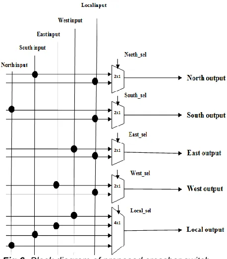
Proposed crossbar switch block diagram is shown in Fig.6. It consist of four input channel in a row i.e. north input, south input, east input, west input and local input, four output channel in column i.e. north output, south output, east output, west output and local output, in internal structure as shown in block diagram it consist four 2x1 MUX where each MUX have two input channel, one output channel and one selection line[41].and it also consist of one 4x1 MUX which has four input channel and four output channel with two selection line[29].
Table.1 Direction of input and output channel
DIRECTION INPUT
CHANNEL
OUTPUT CHANNEL North Direction North input North output South Direction South input South output East Direction East input East output West Direction West input West output Local Direction Local input Local output
Fig.6: Block diagram of proposed crossbar switch
Here by implementing idea of four 2x1 MUX it is proposed that data will only transfer in one direction in each of four input direction, such as from north to south ,south to north, east to west, west to east and in this type of data transmission method transmission path doesn‘t block by any other channel. In this way it provides high speed data transmission between two channels and also contributes to minimize area of cross bar switch. Apart from providing connectivity between directional input and output channel, each four input channel (i.e. east (E), west (W), north (N), and south (S)) is also connected with local output channel to connect intellectual property (IP) to communication network. In our proposed model it is used a 4x1 MUX to connect four directional input channel i.e. north input channel, south input channel, east input channel and west input channel to localoutput channel such as conventional NoC router architecture[29].
962
Proposed digital circuit i.e. a crossbar switch is simulated in Xilinx9.2 ISE, where total delay from input to output port is calculated which is divided in two part i.e. delay due to logic used in circuit and delay due to path of the circuit mathematically we it can be expressed as
ttotal = tlogic + troute
Where
ttotal = total delay from input to output in ns
tlogic = total delay due to logic used in circuit in ns
troute = total delay due to path in ns
Above proposed model is designed by using VHDL language and this design is simulated in Xilinx 9.2 ISE software, outcomes of results, i.e. RTL view of proposed efficient crossbar switch is shown in Fig.5, where all input line, out line and selection line is shown in Fig.5. schematic diagram of result is shown in Fig.6 where it is shown that four 2x1 MUX is connected with four input and output channel and a 4x1 MUX is used to connect four input channel to one output channel. Simulation result of above proposed model is shown in Fig.7. Power, delay and area of proposed model is analysed by using x-power tools of Xilinx software. And result of proposed crossbar switch is compared with conventional and 2-D mesh crossbar switch that is shown in Table.2. Result shows significant improvement in proposed model as compare to 2-D mesh Crossbar switch as well as conventional crossbar switch [6].
IV. RESULTS
Design of proposed crossbar switch has been synthesized and simulated on Xilinx9.2i Spartan3E FPGA Device. RTL view and simulation result of proposed method is shown in Fig.8 and Fig.10 simuntanousaly. Fig.10 shows the results of switching of input to the output at different control signals in the form of wave. Fig.9 shows the schematic view of the proposed crossbar switch. As shown in Fig.7 FPGA consist a slice to implement any Boolean logic and a slice consist of two 4 input LUT (look up table). In conventional crossbar design has 40 slices and 80 no. LUT. In proposed crossbar switch since four 4x1 MUX are replaced by 2x1mux it required only 24 slices and 48 LUT.
In Table.2, indicates the compression of delay, area (area in terms of number of slice LUT‘s) and power of the proposed crossbar switch design with compare to 2-D cross bar switch design [6]. Table.3 gives FPGA Resource utilization by Conventional and Proposed crossbar switch. Proposed cross bar switch has delay due to logic circuit i.e. tlogic=5.515 ns, due
to path i.e. troute=1.629 nsand total delay i.e. ttotal= 7.144 ns as
compared to conventional crossbar switch which has delay due to logic circuit i.e. tlogic= 6.289 ns, delay due to path i.e.
troute=3.720 and total delay i.e. ttotal= 10.009 ns it has 77.2%
delay due to logic circuit and 22.8% due to path as compared to conventional crossbar switch which has62.8% delay due to logic circuit and 37.2% due to path. Total memory usage in proposed crossbar switch is 163400 kilobytes as compare to conventional crossbar switch where memory usage is 163464 kilobytes.
Table.2: Area, delay and power of proposed crossbar switch design and there compression
CROSSBAR SWITCH
AREA(SLICE/LUT COUNT)
POWER DELAY
Conventional
Crossbar switch 40/80 351mw 7.864ns
2-D Cross bar
switch 40/80 14 mw 7.694ns
Proposed
Crossbar switch 24/48 102mw 7.144ns
Table.3: Compression between FPGA Resource utilization of Conventional and Proposed crossbar switch (Spartan 3E)
Resource Available
Conventional Crossbar Switch
Proposed Crossbar Switch Used Utilization Used Utilization
Slice 960 40 4% 24 2%
LUTs 1920 80 4% 48 2%
I OBs 66 90 136% 86 130%
Fig.8: RTL view of proposed crossbar switch design
963
Fig.10: Simulation result for proposed cross bar switch
V. CONCLUSION
In this paper an efficient crossbar switch design is proposed for high speed NoC. Proposed crossbar switch has four 2x1 MUX and a 4x1 MUX as compared to five 4x1 MUX in 2D existing crossbar switch. Simulation results show that delay is reduced by 7.14% and area by 40% as compared to 2-D crossbar switch.
VI. REFRENCES
[1] W. J. Dally and B. Towles, ―Route packets, not wires: on-chip interconnection networks,‖ in Proceedings of the 38th Design Automation Conference, Las Vegas, Nev, USA, pp. 684–689, June 2001.
[2] W. J. Dally and B. P. Towles. Principles and practices of interconnection networks. Morgan Kaufmann Publishers, ISBN: 0122007514, San Francisco, CA, 2004.
[3] J. Nurmi, ―Network-on-chip: A new paradigm for system-on-chip
design,‖ in Proc. IEEE Syst.-Chip, Nov., pp. 2–6, 2005.
[4] B. S. Feero and P. P. Pande, ―Networks-on-chip in a three-dimensional environment: A performance evaluation,‖ IEEE Trans. Compute., vol. 58,no. 1, pp. 32–45, Jan. 2009.
[5] R. Marculescu, U. Y. Ogras, L.-S. Peh, N. E. Jerger, and Y. Hoskote, ―Outstanding research problems in NoC design: System, microarchitecture, and circuit perspectives,‖ IEEE Trans. Comput.-Aided Design Integr. Circuits Syst., vol. 28, no. 1, pp. 3–21, Jan. 2009.
[6] S. Bansal, S. Sharma, and N. Sharma ― Design of Configurable Power Efficient 2-Dimensional Crossbar Switch For Network-on-Chip(NoC )‖ IEEE International Conference On Recent Trends In Electronics Information Communication Technology, India , pp. 1514–1517 May 20-21, 2016.
[7] L. Mingche, G. Lei, S. Wei, and W. Zhiying, ―Escaping from blocking: A dynamic virtual channel for pipelined routers,‖ in Proc. Int.Conf. Complex, Intell., Softw. Intensive Syst., Barcelona, Spain, pp. 795–800,2008. [8] A. Khodwe, V.K. Rajput, C.N. Bhoyar and P. M.
Nerkar, ―Design of Reconfigurable Crossbar Switch
for BiNoC Router,‖ International Journal on Recent and Innovation Trends in Computing and Communication. Volume: 1 Issue: 4, pp 234–240, April 2013.
[9] D. Park, A.Vaidya, A. Kumar and M. Azimi, ―MoDe-X: Microarchitecture of a Layout-Aware Modular Decoupled Crossbar for On-Chip Interconnects,‖ IEEE Transactions On Computers, Vol. 63, No. 3, pp. 622-636, March 2014.
[10]J. Kim, C. Nicopoulos, D. Park, V. Narayanan, M.S. Yousif, and C.R. Das, "A Gracefully Degrading and Energy-Efficient Modular Router Architecture for On-Chip Networks," Proc. 33rd Ann. Int'l Symp. Computer Architecture(ISCA),pp 4-15, 2006. [11]K. lee et al., "Low-Power Network-on-Chip for
High-Performance SoC Design," IEEE Transactions on Very Large Scale Integration (VlSI) Systems, vol. 14, no. 2, pp. 148-160,2006.
[12]G. de Micheli and L. Benini, ―Networks on chip: A new paradigm for systems on chip design,‖ in Proc. DATE,pp. 2–6,2002.
[13]G. Ascia, V. Catania, and M. Palesi, ―Multi-objective mapping for
mesh-based NoC architectures,‖ in Proc. ISSS-CODES, pp.182–187,2004.
[14]K. Goossens, L. Mhamdi and I. V. Senim, ―Internet Router Buffered Crossbars Based On Networks-On-Chip,‖ 12th Euromicro Confrence On Digital System Design/ Architectures, Methods and Tools,pp. 365-374, 2009.
[15]C. H. Hoo and Akash Kumar, ―An Area-Efficient Partially Reconfigurable Crossbar Switch With Low Configuration Delay,‖ 978-1-4673-2256-0, IEEE,pp. 400 – 406,2012.
[16]S. Abovyan, G. Patrosyan and T. Harutyunyan, ―Architecture Of Queued-Free Crossbar For On-Chip-Network,‖ 978-1-4244-9556-6, IEEE,pp.114-121, 2010.
[17]S. Malipatil and Rekha S, ―Design And Analysis of 10 Port Router for Network-On-hip (NoC),‖ International Confrence On Pervasive Computing (ICPC),pp.1-3, 2015.
[18]S. Kumar and A. Srivastava , ―Design And Implementation of Crossbar Switch in NS2,‖ 5th ICCCNT, Hefei, China, pp.11-13, July 2014.
[19]Y. Lee, J. M. Jou and Y. Chen, ―A High-Speed and Decentralized Arbiter Design for NoC,‖ 978-1-4244-3806-8, IEEE pp.350-353,2009.
[20]Ronny Pau and Naraig Manjikian, ―Implementation of a Configurable Router for Embedded Network-On-Chip Support in FPGAs,‖ 978-1-4244-2332-3, IEEE,pp.25-28,2008.
[21]S. Charles, ―Let‘s Route Packets Instead of Wires,‖ Proc. 6th MIT Conf., Advance Research in VLSI, pp. 133-138,1990.
[22]H. S. Wang, L. S. Peh, and S. Malik, ―Power-driven design of router micro architectures in on-chip-networks,‖ In Proceedings of the 36th Annual ACM/IEEE International Symposium on Micro architecture, Washington DC, USA, pp. 105–116 December 2003.
964
selected topics in circuits and systems, Vol.2, No.2, pp. 278-294, June,2012.
[24]Supriya Rao, Supreet Jeloka, Reetuparna Das, David Blaauw, Ronald Dreslinski and Trevor Mudge, ―VIX: Virtual Input Crossbar for Efficient Switch Allocation,‖ DAC 2014, ACM 978-1-4503-2730-5/14/06,pp.1-6, June 1-5, 2014.
[25]M. Oveis-Gharan and Gul N. Khan, ‗Efficient Dynamic Virtual Channel Organization and Architecture for NoC Systems‘, IEEE Transactions On Very Large Scale Integration (VLSI) Systems, Vol. 24, No. 2,pp. 465–478, February 2016.
[26]BP Shrivastava and K Khare "Area and power efficient router design for network on chip" International Journal of Scientific and Research Publications, Volume 3, Issue 5, 1 ISSN 2250-3153,pp.1-5 May 2013.
[27]BP Shrivastava and K Khare "Smart Multicrossbar Router Design In NOC" International Journal of VLSI design & Communication Systems (VLSICS) Vol.4, No.2,pp.75-82, April 2013.
[28]BP Shrivastava and K Khare "Synthesis and Simulation of Enhanced Buffer Router vs. Virtual Channel Router in NOC ON Cadence" World Academy of Science, Engineering and Technology International Journal of Electrical and Computer Engineering Vol:7, No:2,pp. 285-293,2013.
[29]BP Shrivastava and K Khare "Design of Improved Routers for Network on Chip" International Journal of Computer Trends and Technology (IJCTT) – volume 4 Issue 9 pp. 2975-2980,Sep 2013.
[30]K. Shu-Min Li, "CusNoC: Fast Full-Chip Custom NoC Generation"