© 2015 IJSRSET | Volume 1 | Issue 6 | Print ISSN : 2395-1990 | Online ISSN : 2394-4099 Themed Section: Engineering and Technology
Implementation of UART with Error Correction and Error
Detection Capability & Frame Length Selection
Amit Khare*, Nitesh Dodkey
Surabhi Group of Institute, Bhopal, Madhya Pradesh, India
ABSTRACT
This work represents implementation of UART (universal asynchronous receiver transmitter with the error correction and detection capability of one bit with different frame of bits. But the frame of bits should be equal to four bits and can be up to eight bits. In this phenomenon two operating modes can be used in application by the design circuit configuration, first is the normal mode in which one parity bit is added for one bit error detection and the second mode is error correction where single error can be corrected and double error can be detected. By use of this work there is no need of built-in-self test. The error correction used in this design is extended hamming code in which four numbers of hamming bits are added for error correction capability mode. In this configuration the baud rate of transmission and reception can be selected dynamically amongst eight different options. This design configuration is implemented on Field programmable gate array (FPGA), and the target device is Spartan 3E. Keywords: UART, FPGA, Forward Error Correction, Error detection, Baud Rate.
I.
INTRODUCTION
UART is the peripheral for the microprocessor for asynchronous serial communication. It takes a data byte/word at a time from the microprocessor and adds start, stop, parity bit etc., to form a frame. This frame is transmitted bit by bit. Synchronization between transmitter and receiver is achieved by the start and stop bits. This protocol thus adds extra bits (overhead) to the data byte.
Several schemes have been proposed by various researchers in recent years. UART for integration with FPGA has been implemented for reliable data transmission [6]. UART with status register by VHDL implementation has been proposed [2] with the capability of detecting parity error, framing error, overrun error, and break error using status register. UART with a recursive summing filter to remove noise has been proposed by authors of [7]. R. W. Hamming [1] proposed linear block code called hamming code with forward error correction capability of 1 bit.
In this paper, we present a UART with error detecting and correction capability. The inclusion of a hamming encoder in the transmitter section and hamming decoder in the receiver section can correct up to one error and detect up to two errors.
II.
METHODS AND MATERIAL
Proposed Architecture of UART
UART works in asynchronous mode which does not require transmission of clock along with the data. The proposed UART employs a 12 bit frame as shown in figure 1. The character length can vary from 5 to eight bits and hence the frame length can vary from 8 to 11 bits. This works in the two modes. First one is normal mode and the second one is error correction and detection mode. This paper principally deals with the error correction mode.
hamming bits are concatenated in the LSB position with 4 data bits forming 8 bit hamming code. In the transmitter, the data frame is formed with one start bit followed by 8 bits of hamming code, a „1‟, and one stop bit. Start bit is a „0‟ and stop bit is a „1‟. This frame is transmitted by the transmitter bit by bit. When received by the receiver, the overhead are separated from the frame. The hamming code is decoded to correct the error in the received data. Errors up to one can be corrected in this method and two errors can be detected. The data bits after correction are available in parallel form to be accepted by the microprocessor. The frame formats for the proposed UART in the error correction mode and also in normal modes are shown in fig. 1 and 2 below.
Figure 1: Frame Format – Error Correction Mode
Figure 2: Frame Format – Normal Mode
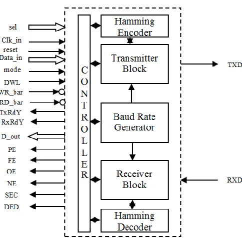
Figure 3 shows the high level block diagram of UART transmitter and receiver with error correction capability. The “clk_in” signal is the system clock which is used to derive the transmission clock and receiver clock to determine baud rate of transmission and reception using baud rate generator. The “reset” signal resets the UART and put the machine in idle mode clearing all the internal registers. The 8 bit data_in the input data lines from the processor and the data from these data lines is transmitted over “TXD” line. When “mode” = 1 then the selected mode is error correction mode and if “mode” = 0 then the selected mode is normal mode. “DWL” is data word length, it is a two bit signal which is used to determine the length of charter. Table 1 define the possible values of DWL.
Table 1 : Word Lengths
DWL Word Length
00 5 bits
01 6 bits
10 7 bits
11 8 bits
Figure 3: High level block diagram – UART
“Wr_bar” is active low input signal from processor which is used to write data to the transmitter of UART. “RD_bar” is the active low input signal from processor which is used to read receiver register of UART. “Txrdy” is the output signal used to interrupt processor, the processor writes next data word in response to this signal. “Rxrdy” is output signal used to interrupt processor; this signal informs the processor about the availability of data byte in receiver register, the processor reads the receiver register in response to this signal. “D_out” is the 8 bit output line to processor. “PE” when high informs about parity error. “FE” when high informs about framing error. “OE” when high informs about overrun error. “NE”, “SED” and “DED” are applicable only in error correction mode. “NE” when high shows no error in received data. “SEC” when high shows the correction of single bit error. “DED” shows the detection of two bit error and it cannot be corrected.
A. Baud Rate Generator
Figure 4: Baud Rate Generator
reception, “clk_in” the system clock, the three bit
“sel” signal determines the baud rate. Table 2
shows the “sel” values with the corresponding baud
rates. Internally divide by n counters
are used to achieve different baud rate. “Reset” signal resets the baud rate generator and initializes internal counters.Table 2: Baud Rate Selection
SEL Baud Rate@ clk_in = 10Mhz
000 57600bps
001 38400bps
010 19200bps
011 9600bps
100 4800bps
101 2400bps
110 1200bps
111 600bps
B. Transmitter
The transmitter block is shown in figure 5. When the “mode” input is zero then the selected mode is normal mode in which only parity bit is generated for error detection. Total 9 bits are generated from this unit, 8 data bits and 1 parity bit. When the “mode” input is one then the selected mode is error correction, in this mode 4 LSB data bits are taken from the data bus input “data_in” and hamming code is applied is to it to from an 8 bit word. Total 9 bits are generated from this unit, 4 hamming bits, 4 data bits and 1 bit is always „1‟. The frame format is shown in figure 1 and 2 respectively. The transmitter hold register (THR) is used to hold the data from the parity encoder or from the hamming encoder. The TSR block does the framing i.e. insertion of start and stop bit to the data word and transmits data serially over “TXD” line on rising edge of “clk_baud”. Also the character length can be varied using DWL only in normal mode. This length is fixed to 8 bits in error correction mode.
Figure 5: Transmitter with Hamming Encoder
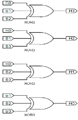
C. Hamming Encoder
The hamming encoder generates an (8,4) extended hamming code called SEC-DED code, which is the extended (8,4) hamming code. The SEC-DED code is the Single Error Correcting and Double Error Detecting code. It can correct one error and can detect up to a maximum of two errors. It is an extension of the (7, 4) hamming code and formed by adding one extra parity bit. Hence the SEC-DED code has 4 data bits(LSB) followed by 4 check bits (hamming bits). The encoder takes 4 data bits giving out 8 bits consisting of the 4 data bits followed by 4 parity bits. Fig. 6 shows the extended (8,4) hamming code generation logic circuit.
Figure 6 : Hamming Encoder
D. Receiver Block
“baud_clk”. Then the assembled data of 9 bits, 8 data bits (variable in case of normal mode depending upon “DWL” signal) and 1 parity bit (always 1 in case of error correction mode) is forwarded to either parity decoder logic or hamming decoder logic depending upon the value of “mode” input signal. The parity decoder logic generates parity error in case of parity error. The hamming decoder logic decodes the input data and checks for any error, if single bit error the error is corrected and data is forwarded to SBUF, also “SED” signal is made high, else if double error are detected then “DED” signal is made high and data is discarded. If no error is detected then the data is forwarded to SBUF and “NE” signal is made high. The SBUF block then generates “rxrdy” signal to inform processor about the arrival of new data byte, the processor reads the SBUF in response to this “rxrdy” signal. Prior to the read cycle if next data byte is arrived then over run error “OE” is generated and UART starts assembling next data byte.
Figure 7 : shows the receiver block of UART
E. Hamming Decoder
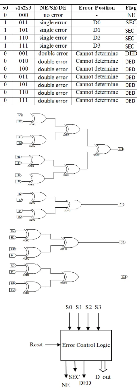
Hamming decoder takes the 9 bit assembled data, discard the 9th bit as it is always „1‟ and used only for the uniformity of data frame size. The remaining 8 bits are has 4 bit of data and 4 bits of check bits which are used to identify errors. If the error is of only 1 bit then it is corrected and if it is of 2 bit then it can only is identified. Respective flags are generated in this process. Figure 8 shows the hamming decoder logic used in this design. s3, s2, s1, s0 bits are generated to identify the location and type of error. Table III shows the possible values of s3-s0 and corresponding meaning.
Table 3 : Error Control Logic
The “d_out” is an 8 bit data to the processor, 4 least significant bits are data and remaining 4 bits are always zeros.
F. Controller
Figure 9 : State Diagram - Transmitter
Figure 9 shows the state machine for the transmitter controller block. At reset machine is in IDLE state, at the arrival of “wr_bar” signal machine moves to either ERROR CORRECTION state or NORMAL state depending upon the value of “mode” signal. Then in these states data frame to be transmitted is formed and then at the arrival of next rising edge of “clk_baud” machine moves to START state, start bit is transmitted in this state. Then machine moves to B0 then B1 and so on, to PARITY and in these states bits are transmitted serially over “txd” line. The number of bits to be transmitted is decided by DWL.
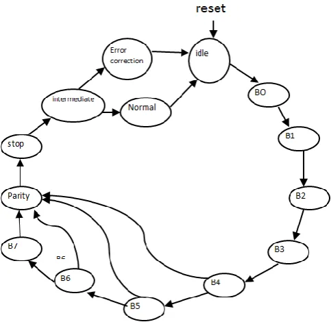
Figure 10: State Diagram - Receiver
Figure 10 shows the state machine for the receiver controller block. At reset the machine is in IDLE state and remains in idle state till the arrival of valid start bit, at the arrival of start bit and next rising edge the machine changes its state to B0 and then to B1, B2, ….B7. In these states the serial data is captured in a RHR register. In PARITY state the data is checked for any parity errors and then in STOP state the framing error signal “FE” is updated. In INTERMIDIATE state the next state is decided depending upon the “mode signal”. Error signals are updated in this state and machine goes into idle state till the arrival of next start bit.
III.
RESULTS AND DISCUSSION
Simulation
In this section simulation of UART transmitter and receiver is presented. We have implemented our design on Xilinx Spartan 3 FPGA and used Xilinx 14.1i CAD tool for simulation, synthesis and implementation. Figure 11 shows the simulation of UART transmitter in normal mode. After the “wr_bar” signal goes the “txrdy” goes low and data is transmitted on rising edge of “clk_baud” over “txd” line serially. The parity bit PB and stop bits are also shown in figure.
Figure 11: Simulation – Transmitter – Normal Mode
Figure 12: Simulation – Receiver – Normal Mode
Figure 13: Simulation – Transmitter – Error correction Mode
the arrival of stop bit “rxrdy” is signal is generated to processor, in response to this signal the processor initiates read cycle and data is transferred to “d_out” and the “rxrdy” signal goes low.
Figure 13 shows simulation of UART transmitter in error correction mode the data is loaded when the “wr_bar” signal goes low, then the incoming data is encoded using extended hamming code, here the encoded data for input bits “0001” is “00010111” and it is transmitted over “txd” line at the rising edge of “clk_baud”.
Figure 14: Simulation UART receiver in error correction mode
Figure 14 shows the simulation of UART receiver in error correction mode. At the arrival of start bit at “rxd” the receiver block starts assembling the data at each rising edge of “clk_baud”. After complete assembling of data, it is checked for any error, in this case no error was received and hence the “NE” flag is raised high. And all the other error flags are kept low.
IV.
CONCLUSION
In this research UART with one bit error correction and two bit error detection mechanism is implemented. The design can operate in two modes, normal mode and error correction mode. Also the baud rate of the design can be selected from eight possible values. The character length (number of data bits) can also be selected from four possible values. The target device used for implementation is Spartan 3 FPGA. The maximum operating frequency is 160 Mhz for this design.
V.
REFERENCES
[1] R. W. Hamming, “Error detecting and error
correcting codes”, The Bell System Technical journal Vol. XXIX, April 1950, Vol. 2, American Telephone and Telegraph company.
[2] Naresh Patel, Vatsalkumar Patel, Vikaskumar
Patel, ”VHDL Implementation of UART with Status Register”, 2012 IEEE International Conference on Communication Systems and Network Technologies, 2012.
[3] Elmenreich W, Delvai M, "Time-triggered
communication with UARTs”, 4thIEEE
International Workshop on Factory Communication Systems, 2002, pp. 97- 104, 2002.
[4] Gallo R, Delvai M, Elmenreich W, Steininger A,
“Revision and verification of an enhanced UART”, 2004, Proceedings, 2004 IEEE International Workshop on Factory Communication Systems, pp. 315- 318, 22-24, Sept. 2004.
[5] Norhuzaimin J, Maimun H.H, "The design of high
speed UART", Asia- Pacific Conference on Applied Electromagnetics (APACE), pp. 20- 21, Dec. 2005.
[6] Fang Yi-yuan, Chen Xue-jun, "Design and
Simulation of UART Serial Communication Module Based on VHDL", 2011 3rd International Workshop on Intelligent Systems and Applications (ISA), pp. 1-4, 28- 29, May 2011. Yongcheng Wang, Kefei Song, "A new approach to realize
UART", 2011 International Conference on
Electronic and Mechanical Engineering and Information Technology (EMEIT), pp. 2749-2752, 2011.
[7] Himanshu Patel, Sanjay Trivedi, R. Neelkanthan,
V. R. Gujraty , "A Robust UART Architecture Based on Recursive Running Sum Filter for Better Noise Performance", Held jointly with 6th International Conference on Embedded Systems, 20th International Conference on VLSI Design, pp. 819-823, Jan. 2007.
[8] Idris, M.Y.I, Yaacob M, "A VHDL implementation
of BIST technique in UART design", 2003 Conference on Convergent Technologies for Asia-Pacific Region (TENCON), pp. 1450-1454, 2003.
[9] Chun-zhi He, Yin-shui Xia, Lun-yao, Wang, "A
universal asynchronous receiver transmitter
design”, 2011 International Conference on Electronics Communications and Control (ICECC), pp. 691-694, 9-11, Sept. 2011.
[10] Prof. Rami Abielmona, “Project UART Design”,