75 |
P a g e
A STUDY OF LOW TO HIGH SWING CONVERTERS
FOR ON-CHIP INTERCONNECTS IN CMOS
VOLTAGE INTERFACE CIRCUITS
Neeraj saini
1, Deepak kedia
2 1M.Tech, VLSI Design & Embedded system,
2Department of Electronics and Communication
Guru Jambheshwar University of Science and Technology, Hisar (India)
ABSTRACT
This paper explores the use of interconnect signaling techniques to improve Delay time for performance and
reduce power consumption of On-chip interconnect. The various Driver–Receiver pairs such as ddc-db, asf-lc,
mj-sib and mj-db for On-chip interconnect with different capacitive load at the output of the circuit are being
explored in detail. A detailed comparison of the driver-receiver pairs for On-chip interconnects line with
differential capacitive load from 0.5pF to 3.0pF and VDD power supply is 3.3V/1.2V has been carried out. These
techniques are widely used to improve the signal bandwidth of interconnect channels and to meet the delay goal
of cross-chip communication.
Keywords: Mentor Graphics 8.2, Xilinx Simulink
I.
INTRODUCTION
Power consumption, delay and noise of global interconnects have become the major factors in deciding how
long CMOS can serve the world’s need for intelligent devices and communication [1],[2]. Due to the scaling
nature of silicon technologies, it is no longer area, but global signaling and power dissipation that have become
the limitations in integrating more functionality on a chip. Unlike local or intermediate interconnects, global
interconnects do not scale down in length, since they communicate signals across a chip [3]. Together with a
lack of new processes and materials based solutions for long interconnects, signaling design on global
interconnects has become an increasingly important issue for circuit and architecture designers. Conventional
repeater insertion techniques have been effective at achieving lower latency and higher data throughput for
On-Chip RC dominated interconnects [4], [5]. However, the insertion of repeaters causes layout placement
blockages that interrupt interconnect lines and circuits beneath. More importantly, the number of required
repeaters increases as optimal repeater insertion spacing decreases with each technology node [6]. The power
dissipation and delay latency associated with repeater themselves start to challenge the power/delay
performance of global interconnects [7]. The Low Voltage Swing technique in CMOS circuit has a signal
receiving unit, a signal processing unit and a driving circuit. The signal receiving unit converts a small
amplitude signal from a bus into a large amplitude signal. The signal processing unit processes the large
amplitude signal. The driving circuit converts the large amplitude signal processed into a small amplitude signal
76 |
P a g e
insertion techniques effectively improve the data rate for long on-chip interconnects by changing the quadraticrelationship between line delay and line length to a linear relationship (Figure 1.1). Up to 80% of on-chip global
interconnects in high performance ICs require repeaters to meet the delay goal. Repeaters divide a long line into
several shorter segments. This makes the coupling distance of long parallel lines shorter and prevents inductive
effects. Significant work has been done on delay, power, or noise optimal repeater insertion techniques.. More
importantly, the number of required repeaters increases as optimal repeater insertion spacing decreases with
each technology node. The power dissipation and delay latency associated with repeater themselves start to
undermine the power/delay performance of global interconnects.
(1/2)RoCoL2 -> (1/2) RoCoL2/K
Quadratic -> Linear
Figure 1.1 Repeater insertion techniques [15].
Speed improvements on long interconnect lines are possible by reduce the energy delay. The driver receiver pair
must have reasonable noise margin is reduced unless a differential approach is used. The π-3 interconnect model
for simulation in this process with CL = 1pF, CW = 1pF and RW = 300Ω. CL is the load capacitance distributed
along the wire, CW is the wire capacitance and RW the wire resistance. The technology 0.35µm process is used
to check the performance of the low swing architecture in a deep sub- micron process.
. Figure 1.2: Interconnect π-3 model [5].
The dynamic switching energy required to drive the line with low swing (ELOW)
ELOW = Ctot. Vdd.Vs (1)
Where Ctot is the total capacitance driver
( CL + CW ), Vdd is the driver power supply voltage and Vs is voltage swing applied over the line.
The total introduced in the line (Vn) is estimated as follows:
VN = KN. VS+ VIN (2)
Where KN. VS accounts for the noise that is proportional to the signal amplitude such as crosstalk and induced
power supply noise and VIN represents the noise sources that are independent of the signal magnitude like
transmitter and receiver offsets. The signal noise ratio (SNR) then:
SNR = 0.5. VS/ VN (3)
It is very effective to reduce the power consumption of global communication by reducing signal swing. The
equation for dynamic power as a function of voltage swing on interconnect is,
Pdyn = α f CL V2 (4)
Where α is the data activity, f is the working frequency, CL is the total of wire and load capacitance, and V is the
77 |
P a g e
problems of interconnections. The bus driver drives a bus line with reduced output swing, VCC/n. The busreceiver amplifies the reduced-swing signal to a full swing signal. With this architecture, the gate-level circuit in
the circuit blocks operates faster because the supply voltage can be higher than that determined by the power
limitation. The key issue for this architecture is to achieve high speed level conversion both from high to low
and from low to high transition.
Figure 1.3: Low-swing interconnects circuit [2].
Figure 1.3 shows the conventional level converter (CLC) represents the traditional way of converting a low –
swing signal back to a full swing one. The driver uses an extra low-voltage supply to drive the interconnect from
zero to VDD. Although the noise margin is reduced, this circuit is very robust against noise, as the receiver
behaves as a differential amplifier and the internal inverter further attenuates some noise through re-generation.
It requires two extra power rails to limit the interconnect swing and uses special low-Vi devices to compensate
for the current-drive loss due to the lower supplies. As the performance of VLSI’s increases, the chip size and
the bus width will also increase and the total wiring capacitance of the bus lines will considerably larger. In
addition to the increase in chip power, another concern for the design of VLSI’s is the reliability problems of
interconnections. It relieves problem due to the reduced charging and discharging current.
II. CMOS driver-receiver pair for On-Chip interconnects
(A) CMOS driver-receiver ddc-db for low- high offset symmetric
Increasing energy budget in the integrated circuits comes from the interconnect wires and associated driver and
receiver circuitries. In some gate array design style power dissipation from the interconnect wires amounts to up
to 40% of the total on –chip power dissipation. On the field programmable gate array fabric the reported power
dissipation from the interconnect wires is up to 90%. To achieve power reduction and energy-delay efficiency
on the global interconnects reducing the voltage swing of the signal on the wire. Reducing the voltage swing
generally comes at the expense of reduced reliability and performance and increase in the driver and receiver
complexity. In order to improve the driving capability, some driver circuits rely on bootstrapping techniques.
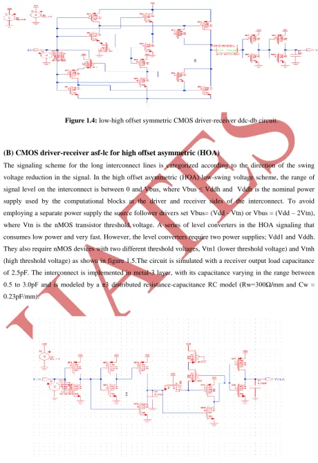
In low-high offset symmetric(LHOS) low-swing voltage signaling scheme, on the other hand, the output
voltage range symmetrically extends between 0 ≤ Vbus1 and Vbush ≤ Vddh. Values of Vbus1 = Vtn and Vbush
= (Vddh - Vtp) are chosen as shown in figure 1.4. Low power LHOS signaling scheme with high driving
capability at the driver side and suitable matching low power level restorer at the receiver side.
driver
receiver Interconnection lines
78 |
P a g e
Figure 1.4: low-high offset symmetric CMOS driver-receiver ddc-db circuit.
(B) CMOS driver-receiver asf-lc for high offset asymmetric (HOA)
The signaling scheme for the long interconnect lines is categorized according to the direction of the swing
voltage reduction in the signal. In the high offset asymmetric (HOA) low-swing voltage scheme, the range of
signal level on the interconnect is between 0 and Vbus, where Vbus ≤ Vddh and Vddh is the nominal power
supply used by the computational blocks at the driver and receiver sides of the interconnect. To avoid
employing a separate power supply the source follower drivers set Vbus= (Vdd - Vtn) or Vbus = (Vdd – 2Vtn),
where Vtn is the nMOS transistor threshold voltage. A series of level converters in the HOA signaling that
consumes low power and very fast. However, the level converters require two power supplies; Vdd1 and Vddh.
They also require nMOS devices with two different threshold voltages, Vtn1 (lower threshold voltage) and Vtnh
(high threshold voltage) as shown in figure 1.5.The circuit is simulated with a receiver output load capacitance
of 2.5pF. The interconnect is implemented in metal-3 layer, with its capacitance varying in the range between
0.5 to 3.0pF and is modeled by a π3 distributed resistance-capacitance RC model (Rw=300Ω/mm and Cw = 0.23pF/mm).
79 |
P a g e
(
C) CMOS driver-receiver mj-sib for low- high offset symmetric
The operation of mj-driver as low state at the output outmj is low we have inn= outmj=low, ou1=high and
ou2=low, MN1, MP2 and MP3 off and MP1 on. In this state, the output is driven low through the diode
connected pair MN4-MN3.Low to high transition at the output outmj due to delay in the feedback loop INV6,
out of nand will go low and out of INV1 go high briefly. This causes MN1 and consequently MP2 to turn on and
strongly pull the output node outmj to high to charge up the output load. In the sib-receiver circuit, the pass
transistor MN1 isolates the internal node2, from the previous stage. Without it the lower potential from the
previous stage causes the current to flow from the Vddh through MP1 back to the driver side. The sib-receiver
uses the inverter INV7 and MN6 transistor to reduce the output pull-down transition time. Splitting the pull-up
for node2 to MP2 and MP3 will help to reduce the load on node3 and reduce energy consumption without
hurting the performance as shown in figure1.6.
(D) CMOS driver-receiver mj-db for low-high offset symmetric
The operation of mj-driver as low state at the output outmj is low we have inn= outmj=low, ou1=high and
ou2=low, MN1, MP2 and MP3 off and MP1 on. In this state, the output is driven low through the diode
connected pair MN4-MN3.Low to high transition at the output outmj due to delay in the feedback loop INV6,
out of nand will go low and out of INV1 go high briefly. This causes MN1 and consequently MP2 to turn on
and strongly pull the output node outmj to high to charge up the output load. In the sib-receiver circuit, the pass
transistor MN1 isolates the internal node2, from the previous stage.
80 |
P a g e
Figure 1.7: Circuit structure for the LHOS CMOS driver-receiver mj-db version.
III. COMPARATIVE SIMULATION RESULTS
The comparison of simulation results for the presented circuits has been drawn. The circuits were analyzed for
various circuit performance parameters. The circuits are optimized individually against the testing benchmark to
get a fair comparison. The performances of them along with the full swing case are tabulated in Table1.1 for the
parameter settings of Vdd=3.3V, CL=0.5 to 3.0pF. In the simulations Vdd is set at 3.3V and the capacitive load
on the interconnect is swept from 0.5 to 3.0pF with the transistor sizes for nMOS (W=2.1u, L=0.5u) and for
pMOS (W=6.1u, L=0.5u) kept constant. Table 1.1 shows the Average power of the four signaling scheme. The
advantage of mj-db driver-receiver with respect to asf-lc that the values are obtained with the driver-receiver
circuit in improved energy dissipation outperforms. Table 1.2 enumerates the components of Delay performance
of the four signaling scheme. The performance of the mj-sib driver-receiver signaling scheme, at the capacitance
of 2.5pF is better than mj-db, mj-sib and LHOS driver-receiver pair.The advantage of mj-sib driver-receiver
with respect to mj-db that the values are obtained with the driver-receiver circuit in improved delay outperforms.
Table 1.1: Average power of various Table 1.2: Delay of driver-receiver pair
driver-receiver pair at different capacitive load.
Capacitive Load CL(pF) Average power(V) LHOS driver-receiver asf-lc driver-receiver mj-sib driver-receiver mj-db driver-receiver
0.5 2.5015 1.951 4.2594 1.4061
1.0 2.5558 1.794 3.8215 1.4083
1.5 2.5933 1.592 3.4847 1.4090
2.0 2.6184 1.227 3.2255 1.4111
2.5 2.6343 0.982 3.0243 1.4089
3.0 2.6394 0.790 2.8627 1.4058
Capacitive Load CL(pF) Delay(ns) LHOS driver-receiver asf-lc driver-receiver mj-sib driver-receiver mj-db driver-receiver
0.5 14.784 18.272 6.7963 13.564
1.0 13.057 17.920 5.9681 12.394
1.5 11.512 17.254 5.4892 11.250
2.0 10.325 16.514 5.2921 10.142
2.5 9.2379 14.223 5.2059 9.1493
81 |
P a g e
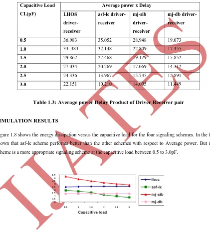
Table1.3 presents the Average power delay product for the four signaling scheme. Reoptimization for thevarious capacitive load energy –delay product it outperforms. However, the values are obtained with
driver-receiver circuits optimized for load capacitance 0.5 to 3.0pF respectively. Reoptimization for the energy-delay
point for 2.5pF results in improved energy-delay performance of mj-db driver-receiver. However, mj-db is an
evident winner, by a significant margin, in terms of both energy consumption and energy-delay product.
Capacitive Load
CL(pF)
Average power x Delay
LHOS
driver-receiver
asf-lc
driver-receiver
mj-sib
driver-receiver
mj-db
driver-receiver
0.5 36.983 35.052 28.948 19.073
1.0 33..383 32.148 22.809 17.455
1.5 29.862 27.468 19.129 15.852
2.0 27.034 20.269 17.069 14.312
2.5 24.336 13.967 15.745 12.891
3.0 22.151 10.210 14.005 11.449
Table 1.3: Average power Delay Product of Driver Receiver pair
SIMULATION RESULTS
Figure 1.8 shows the energy dissipation versus the capacitive load for the four signaling schemes. In the figure
shown that asf-lc scheme performs better than the other schemes with respect to Average power. But mj-db
scheme is a more appropriate signaling scheme at the capacitive load between 0.5 to 3.0pF.
Figure 1.8: Capacitive load versus average power for various drivers –receiver pair in CMOS
on- chip signaling interconnects.
Figure 1.9 presents the delay versus the capacitive load for the four signaling schemes for on-chip interconnects
Low/High voltage swing CMOS driver-receiver pair for driving signals on the global interconnect lines. The
delay performance of the mj-sib driver-receiver is better than other driver-receiver as shown in figure1.9. The
82 |
P a g e
circuit at the capacitive load between 0.5pF to 3.0pF. The delay of the mj-sib receiver and asf-lcdriver-receiver pair is 4.8923 and 12.925 which denotes that mj-sib is having the better performance among the
various deriver-receiver pair in the signaling of data in the On-Chip Interconnection. Figure 1.10 presents the
average power delay product versus the capacitive load for the four signaling schemes. The mj-db driver
receiver performs better than asf-lc, mj-sib, and ddc-db respectively. The delay performance of the mj-sib is the
best among all the signaling schemes.
Figure 1.9: Capacitive load versus delay for various driver-receiver pair
However, mj-db is an significantly better in terms of energy consumption and average delay product. So if the
delay performance is the only design criterion then mj-sib is the most suitable.
Figure 1.10: Capacitive load versus average power x delay for various driver-receiver pair
However if the energy dissipation and average x delay is the design criterion than mj-db is best among the
various driver-receiver pair.
IV.CONCLUSION
This paper deals with tradeoff design techniques that are used in chip signaling design matrix. During
On-chip signaling design matrix, we pay attention towards delay, throughput, power consumption, noise and area by
applying different parameters. The basic and novel idea behind this is to reduce delay and improve power in
On-chip signaling technique. By applying this method we can reduce noise margin and signal swing. The reduction
of noise margin and signal swing will be controlled in the confined domains of the global buses, where noise
levels are tightly controlled by circuit techniques. Finally, the consumption of power is increased on the side of
receiver due to signal swing in the On-chip interconnect lines. We shall control power consumption at receiver
side, so that the delay will be reduced.The various signaling scheme for driving the long interconnects line such
as ddc-db driver-receiver, asf-lc driver-receiver, mj-sib driver-receiver and mj-db driver-receiver pairs are used
83 |
P a g e
mj-db driver-receiver is most superior than other driver-receiver pairs scheme because the total energy-powerconsumption of mj-db driver-receiver is very low.
REFERENCES
[1] Sherif a. tawfik and Volkan Kursun, “ Low Power and High Speed Multi Threshold Voltage Interface
Circuits,” IEEE trans. on VLSI syst., Vol.17, no.5,May2009.
[2] V.kursun, R.M.Secareanu, and E.G. Friedman,” CMOS voltage interface circuit for low power systems,” in
Proc. IEEE Int. Symp. Circuits Syst., May 2002, vol.3, pp.667-670.
[3] R. Golshan and B.Haroun,” A novel reduced swing CMOS Bus interface circuit for High speed low power
VLSI systems,” Proc. of the IEEE international Symposium on circuits and systems, Vol.4, pp.351-354,
June1994.
[4] H.Zhang, V.George, and J.M.Raaey,”Low swing On-Chip Signaling Techniques: Effectivesness and
Robustness,” IEEE Transactions on VLSI Systems, Vol.8, no.3, pp. 264-272, June2000.
[5] Marcos Ferretti,Peter A. Beerel,” Low swing signaling Using a Dynamic Diode-Connected Driver,” solid
state circuit conference, pp.369-372,Sep.2001.
[6] Bouras, et.al,” A High speed low power CMOS clock driver using charge recycling
technique,”ISCAS,May2000.
[7] D.C. Lackey et.al.,” Managing power and performance for system-on-chip designs using voltage island,” in
proc. IEEE/ACM Int. Conf. Comput.Aided Des., Nov.2002, pp. 195-202.
[8] Jose C. Garcia, et.al.,” High performance CMOS symmetric low swing to High swing Converter for on-chip
Interconnect,”IEEE,2007.
[9] J.C Garcia, J.A. Montiel-Nelson and S. Nooshabadi,” High performance CMOS Driver-Receiver pair using
Low swing signaling for low power on-chip interconnects,”2008,IEEE.
[10] J.C Garcia, J.A. Montiel-Nelson and S. Nooshabadi,” CMOS Driver-Receiver pair for Low Swing
Signaling for low energy on-chip interconnects,” IEEE tran. on VLSI systems,Vol.17, no.2, Feb2009.
[11] E.D.Kyriakis-Bitzaros and S.Nikolaidis,”Design of low Power CMOS Drivers based on charge Recycling
Technique,” Proceedings of the IEEE Int. Symposium on circuits and systems, pp. 1924-1927,1997
[12] S. Borkar,” Low Power design Challenges for the decade,” Proceedings of the IEEE/ACM Design
Automation Conference,pp.293-296,June 2001.
[13] J.C Garcia, J.A. Montiel-Nelson and S. Nooshabadi,” Adaptive Low/High voltage Swing CMOS Driver for
On-Chip Interconnects,” Int. sym. On circuits and systems, (ISCAS), May2007,New Orlean, US.
[14] Y.Nakagome et. al.,”Sub 1-V Swing Internal Bus Architecture for future Low power ULSI’s” IEEE
journal of Solid State circuits, Vol.28, no.4, 414-419, April1993.
[15] F. Ishihara, F. Sheikh, and B. Nikolic, “ Level conversion for dual-supply systems,” IEEE Trans. Very
large scale integrated (VLSI) Syst., vol.12, no.2, pp. 185-195,feb2004.
[16] A. Bellaouar, I.S. abu-khater, and M.I.Elmasry,” Low power CMOS/BiCMOS Drivers and receivers for
On-Chip Interconnects,” IEEE J. Solid State Circuits, Vol. 30, no. 6, June1995.
[17] A. Rjoub and O. Koufopavlou,” Efficient Drivers, Receivers and Repeaters for Low Power CMOS Bus
![Figure 1.1 Repeater insertion techniques [15].](https://thumb-us.123doks.com/thumbv2/123dok_us/9215131.1457057/2.595.74.526.206.650/figure-repeater-insertion-techniques.webp)
![Figure 1.3: Low-swing interconnects circuit [2].](https://thumb-us.123doks.com/thumbv2/123dok_us/9215131.1457057/3.595.68.527.167.643/figure-low-swing-interconnects-circuit.webp)