43 |
P a g e
OPTIMIZATION OF LOW POWER ADDER CELLS
USING 180NM TG TECHNOLOGY
Nitasha Jaura
1, Balraj Singh Sidhu
2, Neeraj Gill
31, 2, 3
Department Of Electronics and Communication Engineering, Giani Zail Singh Punjab Technical
University Campus, Bathinda, (India)
ABSTRACT
Continuous scaling of the transistor size and reduction of the operating voltage has led to a significant performance improvement of integrated circuits. Low power consumption and smaller area are some of the most important criterion for the fabrication of Digital Signal Processing (DSP) systems and high performance systems like Laptop & Android based applications in order to achieve the best performance with minimized power consumption. In this paper, Power Dissipation, Transistor Count and Propagation Delay have been minimized as the length and width of NMOS and PMOS are optimized. The proposed circuits are designed and optimized using the Transmission Gate (TG) technology, and the comparative analysis of TG based 8-bit adders has been carried out with 180nm technology, using TANNER EDA tool.
Keywords - Carry Bypass Adder, Carry Look-Ahead Adder, GPDK 180 Nm, Ripple Carry
Adder, TG Based CMOS Logic Design Style.
I. INTRODUCTION
The adder is the most commonly used arithmetic block of the Central Processing Unit (CPU) and Digital Signal
Processor (DSP), therefore its performance and power optimization is of utmost importance. With the
technology scaling to deep sub-micron, the speed of the circuit increases rapidly. At the same time, due to the
increasing chip density, the power consumption per chip also increases. Therefore, in realization of the modern
Very Large Scale Integration (VLSI) circuits, lower power consumption and higher speed are the two
predominant factors which need to be considered. Like any other circuit's design, the design of high-performance
and low- Power adders can be addressed at different levels, such as logic style, architecture, process technology
and the layout. In the proposed paper, Power dissipation, Transistor count and Propagation Delay have been
minimized by optimizing the length and width of NMOS and PMOS transistors.Saradindu et al. [1] initiated the
research work by proposing a full adder built by 28 transistors. As the transistor count is very high, the average
power consumption, leakage power consumption and delay is very high. By making the advanced full adder
circuit, the transistor count, power consumption and propagation delay of the circuit has been reduced. By
applying the different threshold voltages, the power and delay of the new full adder circuit has been optimized.
Further enhancement took place when Vladimir [2] invented a new method for analysis and comparison of ripple
carry full adders by speed on the basis of a new criterion "equal delay capacity" is done. The proposed method
allows quickly and exactly comparing various one-bit adders cell designs by speed for the specific application in
44 |
P a g e
This methodology is applied for minimizing the delay of representative carry-look ahead adders under energyconstraints. The optimality of the result is assessed against the impact of technologyscaling. By analyzing the
impact of the main design choices on adder behavior in the energy–delay space, a set of guidelines can be
established to guide the designer when choosing the architecture of a 64-bit adder.Dan et al. [4] proposed four
low power adder cells used with different XOR and XNOR gate architectures. Basically, two sets of circuit
designs has been presented. One implements full adders with 3 transistors (3-T) XOR and XNOR gates and the
other uses the Gate-diffusion-input (GDI) technique to the full adders. Simulations are run by using H spice
based on 180nm CMOS technology. On the other hand, in comparison with static energy recovery full (SERF)
adder cell module, the four full adder cells demonstrate their advantages, including lower power consumption,
higher speed and smaller area. On the other hand, Sreehari and M.B. Srinivas [5] invented three new 1-bit full
adder cells having a delay of 2T using the existing 3-T XOR and XNOR gates. The power dissipation, delay,
power-delay product and area of these adders have been compared with the existing adders and are found to be
efficient. Reza et al. [6] proposed the introduction of two novel 1-bit full adder cells in dynamic logic styles .
NP-CMOS (Zipper) and multi-Output structures are used to design the adder blocks. Characteristics of dynamic
logic lead to higher speeds than the other standard static full adder cells. Using H-Spice and 0.18µm CMOS
technology exhibits a significant decrease in the cell delay which results in a considerable reduction in the
power-delay product (PDP).Massimo and Gaetano [7] proposed the main topologies of one-bit full adders which
have been compared for speed, power consumption, and power-delay product. The comparison has been
performed on two classes of circuits, the former with minimum transistor size to minimize power consumption,
the latter with optimized transistor dimension to minimize power-delay product. It reveals that except for short
chains of blocks or for cases where minimum power consumption is desired, topologies with only pass
transistors or transmission gates are not attractive. While Sumeer et al. [8] proposed the designs for 1-bit full
adder cell featuring hybrid CMOS logic style. These designs were based on a novel XOR-XNOR circuit that
simultaneously produces XOR and XNOR full-swing outputs and outperforms its best counterpart showing 39%
improvement in PDP. The new XOR-XNOR circuit displays superior performance as compared to the best
competitor. The improvement in terms of PDP obtained by the best full-adder cell as compared to the best
standard design, amounts to 24%. Further implementations in this work was carried out byS.Wairya et al. [9] in
which a novel design to realize full adder circuit was implemented. Basically, the approach was based on
OR-XNOR design full adder circuits in a single unit. Objective of this work was to investigate the power, delay and
power delay product of low voltage full adder cells in different CMOS logic styles. Simulation results, depicts
the superiority of the proposed adder circuit against the conventional CMOS, Hybrid, Bridge, XOR-XNOR
adder circuits in terms of average power consumption, propagation delay and PDP. The design was
implemented on GPDK 90 nm technology, processing models in Cadence Virtuoso Schematic Composer at
1.5V. In this paper, different adder logic styles have been implemented, simulated, analyzed and compared.
Using the adder categorization and hybrid-CMOS design style, many full adders were conceived. The
characteristics of the adder circuits are compared against previous designed adders based on the average power
consumption, propagation delay and PDP. The research efforts of the past years in the field of digital electronics
have been directed towards the low power of digital systems. The improvement in battery performance indicates
power dissipation is one of the most critical parameter. Hence three most widely accepted parameters to measure
45 |
P a g e
dissipation. There are three major sources of power consumption in digital CMOS circuits, which are summarizedin the following equation (1) :-
(1)
The first term represents the switching component of power, where C is the load capacitance, fclk is the clock frequency and α0→1 is the node transition activity factor. The second term is due to the direct path short circuit
currents, where Isc , is the short circuit current which arises when both the NMOS and PMOS transistors are simultaneously active, conducting current directly from supply to ground. Finally, leakage current, Ileakage , which can arise from substrate injection and sub threshold effects, is primarily determined by fabrication technology
considerations. However, supply voltage reduction is the most effective way to reduce the power consumption,
such a reduction requires new design methods for low-voltage and low power integrated circuits. Since an
average of 15-20% of the total power is dissipated in glitching, low power can also be achieved by reducing the
glitches of the circuit. The deep submicron devices gives CMOS VLSI design a great chance to operate at higher
speed, especially for digital signal processing. In our study, novel designs for a full adder has been proposed and
authenticated. All nodes in the proposed full adders have a full-voltage swing and there is no static short-circuit
current problem.
A brief overview of the various CMOS style full adder circuits is discussed below:-
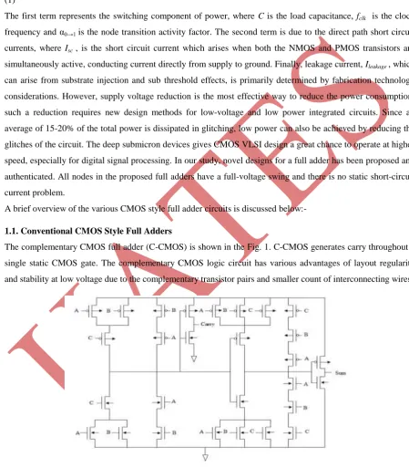
1.1. Conventional CMOS Style Full Adders
The complementary CMOS full adder (C-CMOS) is shown in the Fig. 1. C-CMOS generates carry throughout a
single static CMOS gate. The complementary CMOS logic circuit has various advantages of layout regularity
and stability at low voltage due to the complementary transistor pairs and smaller count of interconnecting wires.
Fig. 1 C-CMOS Full Adder Cell
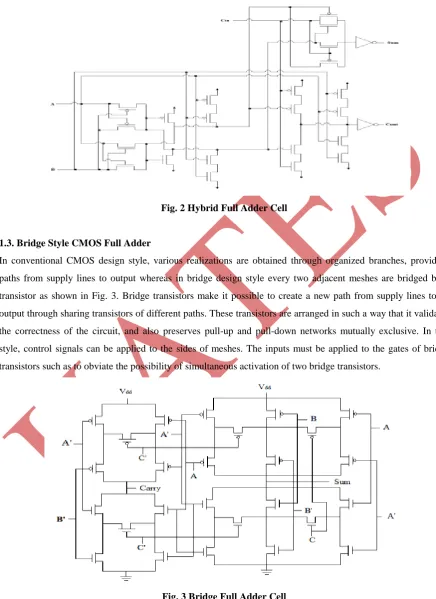
1.2. Hybrid Style Full Adders
Some adder design styles use more than one logic style for their implementation. This is known as the
Hybrid-CMOS logic design style. Hybrid full adder is shown in Fig. 2. which is designed with pass logic circuit which
46 |
P a g e
supply voltage. It uses 26 transistors but has the full swing logic, balanced output and an efficient outputdrivability. All hybrid designs use the best available modules which are implemented using different logic styles
and enhance those available modules in order to build a low power full-adder cell.
Fig. 2 Hybrid Full Adder Cell
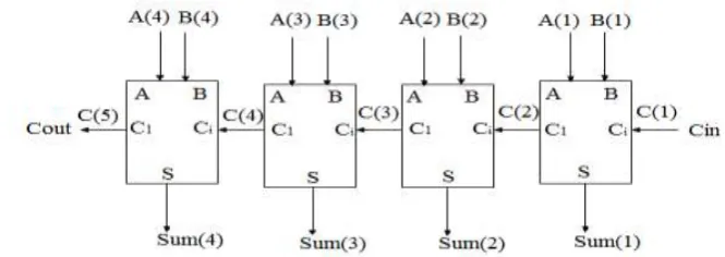
1.3. Bridge Style CMOS Full Adder
In conventional CMOS design style, various realizations are obtained through organized branches, providing
paths from supply lines to output whereas in bridge design style every two adjacent meshes are bridged by a
transistor as shown in Fig. 3. Bridge transistors make it possible to create a new path from supply lines to an
output through sharing transistors of different paths. These transistors are arranged in such a way that it validates
the correctness of the circuit, and also preserves pull-up and pull-down networks mutually exclusive. In this
style, control signals can be applied to the sides of meshes. The inputs must be applied to the gates of bridge
transistors such as to obviate the possibility of simultaneous activation of two bridge transistors.
Fig. 3 Bridge Full Adder Cell
II. PROPOSED WORK
Saradindu Panda, N. Mohan and C.K. Sarkar implemented a new adder design style with reduced transistor
47 |
P a g e
reduced Power Dissipation from the previous circuits with optimized channel length and width of NMOS andPMOS transistors.
The below circuit in the previous base paper [9] produces very high power dissipation and propagation delay,
but the circuits re-designed in our proposed work after the optimization of channel length and width produces
less power dissipation and propagation delay as compared to the previous base paper results.
Fig. 4 Schematic Of Full Adder Circuit
Adder is the most commonly used arithmetic block of the CPU and DSP, therefore its performance and power
optimization is of utmost importance. For arithmetic applications, following three different logic styles are used
for a full adder design to achieve best performance results for adder design.In the proposed work, following
three types of the adder circuits have been designed :-
1. Ripple Carry Adder
2. Carry Look-ahead Adder
3. Carry Bypass Adder
Now, the brief description of the above mentioned adders is explained below :-
2.1. Ripple Carry Adder
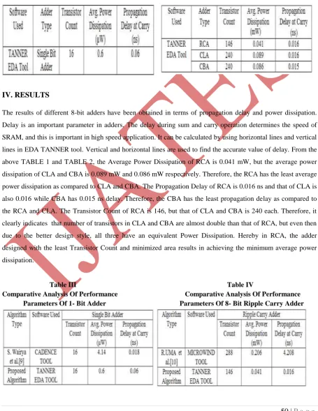
In the Fig. 5, the block diagram of ripple carry adder. Here, the full adder is built by 18 transistors by using TG
technology [1]. In this circuit design process, all simulations are run using Micron Technology’s 0.18 μm process
models with typical n-channel and p-channel drive, a 1.8 V power supply. In the schematics, all logic styles are
designed using a different gate width for NMOS and PMOS and a minimum length of 0.18 μm for NMOS and
PMOS. With the help of below block diagram 8-bit ripple carry adder is developed. In the circuit there are three
inputs A, B, C and two outputs sum and carry.
48 |
P a g e
2.2. Carry Look-ahead Adder
In the Fig. 6, the block diagram of carry look ahead adder is shown. Amita and Mrs. Nitin Sachdeva
implemented the carry look-ahead adder, built by 30 transistors by using TG technology. In this circuit design
process all the simulations are run using Micron Technology’s 0.18 μm process models with typical n-channel
and p-channel drive, a 1.8 V power supply. In the schematics all logics are designed using a different gate width
for NMOS and PMOS and a minimum length of 0.18 μm for NMOS and PMOS. With the help of below block
diagram 8-bit carry look-ahead adder is developed. In the circuit there are three inputs and two outputs.
Fig. 6 Block Diagram Of Carry Look-Ahead Adder
2.3. Carry Bypass Adder
In the Fig. 7, the block diagram of carry bypass adder is shown. Amita and Mrs. Nitin Sachdeva implemented the
2-bit carry bypass adder by 60 transistors by using TG technology. In this design process all simulations are run
using Micron Technology’s 0.18 μm process models with typical n-channel and p-channel drive, at 1.8 V power
supply. In the schematics, all logics are designed using a different gate width for NMOS and PMOS and a
minimum length of 0.18 μm for NMOS and PMOS. With the help of below block diagram, 8-bit carry bypass
adder is developed. In the circuit there are three inputs A, B, C and two outputs sum and carry.
49 |
P a g e
III. SOLUTIONS AND METHODOLOGY
The comparison in our proposed work has been carried out both by considering the circuits with minimum
transistor count, to minimize the power consumption, and with transistors sized by optimized channel length and
width. Power consumption is a function of load capacitance, frequency of operation, and supply voltage. A
reduction of any one of these is beneficial. A reduction in power consumption provides several benefits. Less
heat is generated, which reduces problems associated with high temperature, such as the need for heat sinks. The
minimization of the two parameters i.e. the Average Power Consumption and Propagation Delay are the main
objectives for designing the RCA, CLA and CBA circuits. Therefore, by optimizing the parameters and with the
use of algorithms led to achieve the required simulation waveforms.
3.1. Algorithm Used
Select the 180 nm technology.
Specify the desired transient range of the desired waveforms to be displayed. Mention all the specified inputs and the outputs of the designed circuit.
Calculate the average power consumption by the coinciding point of Vdd and ground. Measure the delay by assigning a specific value of trigger and target.
3.2. Parameter Tuning
With the use of 180 nm technology, the channel length of all the desired circuits is fixed i.e. 0.18µm as the
standard reference value. Now, in order to fix the value for the channel widths of both NMOS and PMOS
transistors we calculate β, where β = (channel length / 2 )
Hence, β = ( 0.18 / 2 ) = 0.09 µm
WNMOS = 3 × β and, WPMOS = 3 × W
NMOS
= 3× 0.09 = 3× 0.27
= 0.27 µm = 0.81 µm
Hereby, setting the above mentioned values of channel length and width of NMOS and PMOS transistors,
as the starting limit and varying the widths of NMOS and PMOS transistors within a specific range as listed :-
0.27 µm ≤ WNMOS ≤ 0.97 µm and, 0.81 µm ≤ WPMOS
≤2.0 µm
Therefore, by varying both WNMOS and WPMOS within the above assigned limits, the final optimized
parameters are obtained which corresponds to the best results with minimized power dissipation and propagation
delay.
3.3. Optimized Parameters (for 1-bit Adder Cell) :-
Channel Length = 0.18 µm
Width of NMOS = 0.64 µm
Width of PMOS = 1.7 µm
With referenced voltage Vdd = 0.8V
50 |
P a g e
Channel Length = 0.18 µmWidth of NMOS = 0.8 µm
Width of PMOS = 2.1 µm
With referenced voltage Vdd = 1.2V
Below tables depicts the optimized performance parameters of the adders:-
Table I Table II
Performance Parameters Of 1 Bit Adder Performance Parameters Of 8 Bit Adders
IV. RESULTS
The results of different 8-bit adders have been obtained in terms of propagation delay and power dissipation.
Delay is an important parameter in adders. The delay during sum and carry operation determines the speed of
SRAM, and this is important in high speed application. It can be calculated by using horizontal lines and vertical
lines in EDA TANNER tool. Vertical and horizontal lines are used to find the accurate value of delay. From the
above TABLE 1 and TABLE 2, the Average Power Dissipation of RCA is 0.041 mW, but the average power
dissipation of CLA and CBA is 0.089 mW and 0.086 mW respectively. Therefore, the RCA has the least average
power dissipation as compared to CLA and CBA. The Propagation Delay of RCA is 0.016 ns and that of CLA is
also 0.016 while CBA has 0.015 ns delay. Therefore, the CBA has the least propagation delay as compared to
the RCA and CLA. The Transistor Count of RCA is 146, but that of CLA and CBA is 240 each. Therefore, it
clearly indicates that number of transistors in CLA and CBA are almost double than that of RCA, but even then
due to the better design style, all three have an equivalent Power Dissipation. Hereby in RCA, the adder
designed with the least Transistor Count and minimized area results in achieving the minimum average power
dissipation.
Table III Table IV
Comparative Analysis Of Performance Comparative Analysis Of Performance
Parameters Of 1- Bit Adder Parameters Of 8- Bit Ripple Carry Adder
51 |
P a g e
Table V Table VI
Comparative Analysis Of Performance Parameters Comparative Analysis Of Performance Of 8-Bit Carry Look-Ahead Adder Parameters Of 8-Bit Carry Bypass Adder
The simulations represents for an adder cell as well as different 8 bit adders are obtained in TANNER tool in the
following section with A, B, C as inputs and Sum, Carry as outputs.
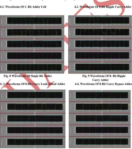
4.1. Waveforms Of 1- Bit Adder Cell 4.2. Waveforms Of 8-Bit Ripple Carry Adder
Fig. 8 Waveforms Of Single Bit Adder Fig. 9 Waveforms Of 8- Bit Ripple Carry Adder
4. 3. Waveforms Of 8-Bit Carry Look-Ahead Adder 4.4. Waveforms Of 8-Bit Carry Bypass Adder
52 |
P a g e
V. CONCLUSIONS
In this proposed work, the comparative performance analysis of the 1- bit full adder cell with 180 nm technology
has been carried out. The comparison has been performed on average power dissipation, propagation delay and
transistor count. The performance analyses, waveforms showing simulation results and comparison have been
depicted in Section III and Section IV. The achieved results reveal that there is an enormous decrease in the
average power dissipation in the proposed circuit. However, the transistor count remains the same with an
approximately equivalent propagation delay at carry, when compared with the research efforts of the past years.
Similarly, the performance parameters in case of all the 8- bit full adders i.e. RCA, CLA and CBA when
compared, reveals that there is a huge reduction in all the three parameters i.e. transistor count, average power
dissipation and propagation delay. Thus, the result indicates that CBA is the fastest full adder topology with
minimum propagation delay even with maximum transistor count amongst RCA, CLA and CBA. Hereby it is
concluded that average power dissipation and propagation delay in TG based adders are very less as compared
to conventional CMOS and other circuits. Therefore, it is concluded that RCA consumes the minimum power
due to least number of transistors used in the circuit design. Even the Propagation Delay of RCA is almost
comparable with CLA and CBA, and with minimum Average Power Dissipation RCA is the best amongst all.
REFERENCES
[1] Saradindu Panda, N. Mohan Kumar, C. K. Sarkar, (2009), “Transistor Count Optimization Of Conventional
CMOS Full Adder And Optimization Of Power And Delay Of New Implementation Of 18 Transistor Full
Adder By Dual Threshold Node Design With Submicron Channel Length”, International Conference On
Computers And Devices For Communication, pp. 978-981.
[2] Vladimir V. Shubin, (2010), “Analysis And Comparison Of Ripple Carry Full Adders By Speed”, XI
International Conference And Seminar EDM', pp. 132-135.
[3] Radu Zlatanovici, Sean Kao, and Borivoje Nikolic, (2009), “Energy–Delay Optimization Of 64-bit
Carry-Look Ahead Adders With a 240 ps 90 nm CMOS Design Example”, IEEE Journal Of Solid-State Circuits,
pp. 569-583.
[4] Dan Wang, Maofeng Yang, Wu Cheng, Xuguang Guan, Zhangming Zhu, Yintang Yang, (2009) “Novel
Low Power Full Adder Cells In 180nm CMOS Technology”, ICIEA, pp. 430-433.
[5] Sreehari Veeramachaneni, M.B. Srinivas, (2008), “New Improved 1-bit Full Adder Cells”, IEEE, pp.
000735-000738.
[6] Reza Faghih Mirzaee, Mohammad Hossein Moaiyeri, Keivan Navi, (2010), “High Speed NP-CMOS And
Multi-Output Dynamic Full Adder Cells”, International Journal Of Electrical And Electronics Engineering,
pp. 304-310.
[7] Massimo Alioto, Gaetano Palumbo, (2002), “Analysis And Comparison On Full Adder Block In Submicron
Technology”, IEEE , pp. 806-823.
[8] Sumeer Goel, Shilpa Gollamudi, Ashok Kumar and Magdy Bayoumi, (2004), “On The Design Of
Low-Energy Hybrid CMOS 1-bit Full Adder Cells”, IEEE, pp. (ii-209)-(ii-2).
[9] S. Wairya, Himanshu Pandey, R. K. Nagaria and S. Tiwari, (2010), "Ultra Low Voltage High S peed 1-Bit
53 |
P a g e
[10]R.UMA, Vidya Vijayan, M. Mohanapriya, Sharon Paul, (2012), "Area, Delay and Power Comparison ofAdder
[11]Topologies", International Journal of VLSI design and Communication Systems, vol. 3,pp. 153-168.
[12]H. Bui, Y. Wang, Y. Jiang, (2002), “Design and analysis of low-power 10-transistor full adders using novel
xor–xnor gates”, IEEE transactions on circuits and systems analog and digital signal processing, vol. 49,