Int. J. of Engg. Sci. & Mgmt. (IJESM), Vol. 3, Issue 1: Jan.-Mar.: 2013, 80-85
INTERNATIONAL JOURNAL OF ENGINEERING SCIENCES
&
MANAGEMENT
TIME OPTIMIZED PROGRAMMABLE MEMORY BUILT-IN SELF TEST FOR EMBEDDED RAM
Sonal Sharma*1, Mr. Vishal Moyal2
*1
ME (VLSI design) SSCET, Bhilai, India
2
SSITM, Bhilai, India
ABSTRACT
In the embedded technology today, memories are the universal components. ROM, SRAM, DRAM or flash memory, any one or a combination can be found in almost all system chips. With the onset of the deep-submicron VLSI technology, the density and capacity of the memory is growing. The wide use of embedded memory forms the basis of emerging new architecture and technologies. However providing a cost effective test solution for these on-chip memories is becoming a challenging task. Memory BIST over the recent times has proven to be one of the cheapest and widely used techniques to perform memory testing. In this research, FSM based programmable memory BIST architecture is proposed which can select March algorithms to test the memory. March algorithms are test algorithms used to test memory because of their high fault coverage and less complexity. Experimental results show that the proposed architecture has reduced simulation time, increased work frequency and improved flexibility.
INTRODUCTION
The exponential increase in density creates great challenge for memory testing. First of all, as the feature size of components shrinks, the sensitivity to faults increases and the faults become more complex. Secondly, since test time grows at least linearly as the number of storage elements per chip increases, the test cost becomes more significant as the cost per transistor drops. Recent development in system-on-chip (SOC) technology makes it possible to incorporate large embedded memories into a chip [1],[2]. On the other hand, it also complicates the test process, since usually the embedded memories cannot be controlled from the outside environment.
Corresponding Author* Email-
Int. J. of Engg. Sci. & Mgmt. (IJESM), Vol. 3, Issue 1: Jan.-Mar.: 2013, 80-85 consists of test circuits that apply, read and
compare test patterns designed to expose defects in the memory device. There exist a variety of industry-standard MBIST algorithms, such as the "March" algorithm, the checkerboard algorithm and the varied pattern background algorithm [8]. In order to perform a high quality test, the memory built-in self test (MBIST) has emerged as a valuable choice due to very regular test patterns and expected responses that can be generated, compressed and stored by using a relatively simple testing circuitry [9]. In this work, a programmable FSM based memory built-in self test architecture is developed using the structured design methodology. The proposed memory BIST supports 8 different test algorithms to test the embedded RAM.
MARCH ALGORITHMS
Notations and March Element Codes: A March test consists of a sequence of March elements; a March element consists of a sequence of operations which are all applied to a given cell, before proceeding to the next cell. The way one proceeds to the next cell is determined by the address order which can be an increasing address order (increasing addresses from cell 0 to cell n- 1), denoted by the '↑' symbol, or a decreasing address order, denoted by the '↓' symbol. The '↓' address order has to be the exact inverse of the '↑' address order. For some March elements the address order can be chosen arbitrarily, this will be indicated by the '↕' symbol. An operation, applied to a cell, can be a 'w0', a 'wl', an 'r0' or an 'rl' operation. A complete march test is delimited by the '{...}' bracket pair; while a March element is delimited by the '(...)' bracket pair [10]. March element codes of all march algorithms used in the proposed
work are listed in the table 1. The proposed memory BIST architecture supports eight March algorithms. Therefore, the selection line has 3 bits and each new combination of bits supports different algorithm. These algorithms will be selected and sent by automated test equipment.
Table 1. March Element Codes of Test Algorithms
S No. Algorithm March Element Code
1 Mats Plus {↕(w0); ↑(r0,w1);
↓(r1,w0)}
2 March X {↕(w0); ↑(r0,w1);
↓(r1,w0);↕(r0)}
3 March C
Minus
{↕(w0); ↑(r0,w1);
↑(r1,w0); ↓(r0,w1);
↓(r1,w0); ↕(r0)}
4 March A {↕(w0);↑(r0,w1,w0,w1);
↑(r1,w0,w1);
↓(r1,w0,w1,w0);
↓(r0,w1,w0);}
5 March B {↕(w0);
↑(r0,w1,r1,w0,r0,w1);
↑(r1,w0,w1);
↓(r1,w0,w1,w0);
↓(r0,w1,w0)}
6 March U {↕(w0);↑(r0,w1,r1,w0);
↑(r0,w1);
↓(r1,w0,r0,w1);
Int. J. of Engg. Sci. & Mgmt. (IJESM), Vol. 3, Issue 1: Jan.-Mar.: 2013, 80-85 7 March LR {↕(w0);↓(r0,w1);
↑(r1,w0,r0,w1);
↑(r1,w0);
↑(r0,w1,r1,w0); ↑(r0)}
8 March SS {↕(w0);
↑(r0,r0,w0,r0,w1);
↑(r1,r1,w1,r1,w0);
↓(r0,r0,w0,r0,w1);
↓(r1,r1,w1,r1,w0);
↕(r0)}
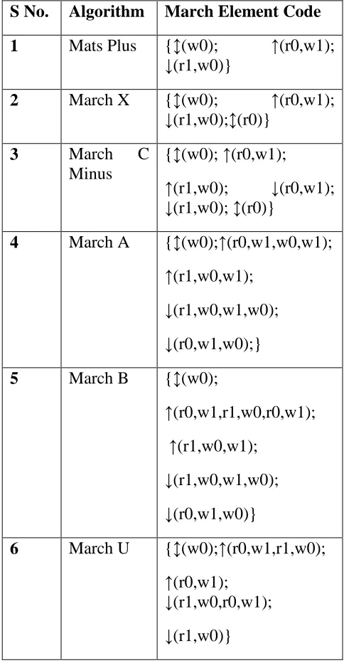
Description of FSM for March SS Algorithm:
Figure 1. FSM of March SS Algorithm
The first state of this algorithm is 'Idle' state, indicating that, there is no BIST operation being performed. The 'Idle' state will continue until 'bist_en' signal remains '0'.
The BIST operation starts as soon as 'bist_en' signal changes to '1'. This state is represented by 'S0'. Under this algorithm the first operation is 'w0' which means that there is a write '0' operation being performed. When 'w0' operation is performed on 'S0', 'wr_comp' signal changes to '1' and the FSM enters a new state 'S1'. In 'S1' state there are five elements which are 'r0', 'r0', 'w0', 'r0' and 'w1'. In this state, a counter is used to indicate the completion of any operation. At first counter will be reset to '000', when first operation 'r0' will be performed then counter will be incremented by '1'. After that, rest of the operations of ‘S1’ state will be performed and counter will be incremented for each operation. When all five operations will be performed, 'rd_comp' and 'wr_comp' signals become '1' and the counter is set to '100', then the FSM will switch to 'S2' state. Similarly all the operations for the subsequent states are performed in the same manner. Finally the 'Idle' state is achieved when the last operation of ‘S5’ state is performed
PROPOSED PROGRAMMABLE
MBIST ARCHITECTURE
Int. J. of Engg. Sci. & Mgmt. (IJESM), Vol. 3, Issue 1: Jan.-Mar.: 2013, 80-85 Figure 2. RTL View of Programmable MBIST
Simulation of Programmable MBIST:
Figure 3. Simulation of Programmable MBIST
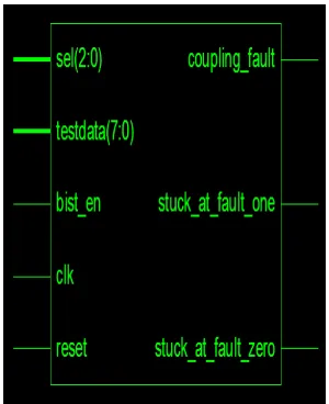
Figure 2 shows simulation of proposed PMBIST. The selection line is given '000' to select the Mats plus algorithm. Input 'bist_en' is set to '1' to start the operation of PMBIST. Signal 'one_zerotemp' is assigned '1' to perform write '1' operation onto the embedded RAM. First, signal 'r_wrtemp' is set to '1' to enable write operation to the RAM and then set to '0' to enable read operation. Output 'faultdetect' compares the test data given to the comparator and the data read from the RAM. Test data is given as '11111111' to the comparator and the data read from RAM is '11111111'. As both the values are same, 'faultdetect' becomes '0'. All other outputs 'stuck_at_FT1',
'stuck_at_FT0' and 'coupling_fault' will also be '0'.
RESULTS & DISCUSSION
Table 2 depicts the simulation time and frequency for the programmable MBIST and March algorithms. Based on these findings it is safe to conclude that the proposed architecture has reduced the simulation time by increasing the execution frequency.
Table 2. Simulation time for March Algorithms
Algorithm tmin(ns) of Proposed work
fmax(MHz) of Proposed work
MATS Plus 3.5 287
March X 3.4 297
March C- 4.5 223
March A 4.5 224
March B 4.6 219
March U 5.1 196
March LR 4.2 239
March SS 4.1 241
PMBIST 7.735 129
CONCLUSION
Int. J. of Engg. Sci. & Mgmt. (IJESM), Vol. 3, Issue 1: Jan.-Mar.: 2013, 80-85 DRAM, SRAM and ROM) because each
memory type requires different test algorithm. Proposed work achieves reduced simulation time and high frequency but the area overhead could not be reduced significantly.
REFERENCES
[1] J. van de Goor and A. Offerman, “Towards a uniform notation for memoty tests,” in Proc. European Design and Test Conf., 1996, pp. 420-427.
[2] V. G. Mikitjuk, V.n. Yarmolik, and A.J. van de Goor,“RAM testing algorithms for detecting multiple linked faults,” in Proc. European Design and Test Conf., 1996, pp. 435-439.
[3] P. H. Bardell and W. H McAnney, “Built-in test for RAMs,” IEEE Design & Test of Computers, Vol. 5, No. 4, pp. 29-36, Aug. 1988.
[4] V. D. Agrawal, C. R. Kime, and K. K. Saluja, “A tutorial on built-in self-test. I. Principles,” IEEE Design & Test of Computers, Vol. 10, No. 1, pp.73-82, Mar. 1993
[5] V. D. Agrawal, C. R. Kime, and K. K. Saluja, “A tutorial on built-in self-test. 2. Principles,” IEEE Design & Test of Computers, Vol. 10, No. 2, pp. 69-77, March 1993.
[6] S. Park, K. Lee, C. Im, N. Kwak, K. Kim, Y. Choi, “Designing built-in self-test circuits for embedded memories test,” in Proc. AP-ASIC 2000, 2nd IEEE Asia Pacific Conf., pp. 315-318.
[7] https://www.classle.net/content-page/overview-bist
[8] http://www.siliconfareast.com [9] Mukherjee, Nilanjan; Pogiel,
Arthur; Rajski, Janusz; Tyszer, Jerzy " High Volume Diagnosis in Memory BIST Based on Compressed
Failure Data"Computer-Aided Design of Integrated Circuits and Systems, IEEE, 2010, Volume: 29,
Issue: 3
Page(s): 441 - 453.