Controlling the Both DC Boost and AC Output Voltages of a
Z-Source Inverter Using Neural Network Controller with
Minimization of Voltage Stress Across Devices
D. Arab Khaburi* and H. Rostami**
Abstract: This paper presents a method to control both the dc boost and ac output voltages of Z-source inverter using neural network controllers. The capacitor voltage of the Z-source network has been controlled linearly in order to improve the transient response of the dc boost voltage of the Z-source inverter. The peak value of the line to line ac output voltage is used to control and keep the ac outputs to their desired values. A modified space vector pulse-width-modulation method is also applied to control the shoot-through duty ratio for boosting dc voltage. This modified method lets to minimize the dc voltage stress across the inverter switches. The neural network control technique is verified with simulation results and compared with the traditional PI controller responses.
Keywords: Power Converters, Z-Source Inverter, Space Vector PWM, Neural Network.
1 Introduction1
Power electronic inverters are increasingly being used in modern energy conversion systems, including uninterruptible power supplies, motor drives and active interfaces for localized and distributed generation. Most of these applications would require the inverters to have both voltage-buck and boost capabilities for riding through load current and supply voltage variations [1], [2]. A common way of implementing buck-boost inverters is to cascade a dc-dc converter to either a buck voltage source or boost current source inverter to form a two-stage power conversion solution, but this cascaded topology usually results to increase system complexity and reduces reliability. The Z-source inverter described in [3] overcomes the conceptual and theoretical barriers and limitations for the traditional inverters and provides a novel power conversion concept.
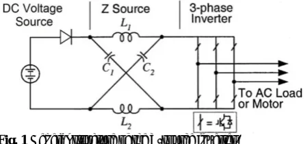
Figure 1 shows the general Z-source inverter (ZSI) structure. The Z-source inverter employs a unique impedance network to couple the inverter main circuit to the dc power supply.
This two-port impedance network consists of a split-inductor L1 and L2 and capacitors C1 and C2 connected
Iranian Journal of Electrical & Electronic Engineering, 2011. Paper first received 25 Aug. 2010 and in revised form 12 Feb. 2011. * The Author is with the Center Of Excellence for Power Systems Automation and Operation, Department of Electrical Engineering, Iran University of Science and Technology (IUST), Tehran, Iran. E-mail: [email protected]
** The Author is with the Department of Electrical Engineering, Khameneh Branch, Islamic Azad University, Khameneh, Iran.
in X shape [4]. In Fig. 1, the three-phase Z-source inverter bridge has nine permissible switching states (vectors) unlike the three-phase V-source inverter that has eight. The V-source inverter has six active vectors and two null vectors. However, the three-phase Z-source inverter bridge has one extra zero state when the both devices of any leg are gated on. This third zero state is called the shoot-through state, which can be generated by seven different ways: shoot-through via any one phase leg, combinations of any two phases leg, and all three phase legs. The Z-source network makes the through zero state possible. This shoot-through zero state provides the unique buck-boost feature to the inverter [5]-[7].
All the traditional pulse-width-modulation (PWM) schemes can be used to control the Z-source inverter and their theoretical input-output relationships still hold. The carrier-based PWM control methods are simple boost control method, maximum boost control method [8], and maximum constant boost control method [9] respectively. Since space vector PWM techniques are more suitable to control the shoot-through duty ratio in the Z-source inverter, it has been developed in recent papers. This paper aims to achieve good performance of both the dc boost and the ac output voltage control of the Z-source inverter using neural network controllers and comparing the obtained results with traditional PI controller.
An algorithm is proposed to linearly control of the capacitor voltage in order to improve the transient response of the dc boost voltage.
Fig. 1 General structure of the Z-source inverter.
The peak value of line to line ac output voltage is used to control the output voltage and keep it to its reference value. A modified space vector PWM is also used to control effectively the shoot-through duty ratio for boosting dc capacitor voltage. Using this modified method, the dc voltage stress across the inverter switches is also minimized.
2 Designing of Impedance Network Parameters Since in voltage source and current source inverters, PWM method or other switching methods are applied without any shoot-trough state, then the capacitor voltages, VC1 and VC2, are constants and equal to Vdc.
Therefore, in this case, the inductances L1 and L2 have a
dc current. But in Z source inverters, these inductances are used to limit the current ripples and increase voltage level in non-shoot-through states. In shoot-through states, currents of these inductances increase linearly and their voltages, VL1 and VL2, are equal to the
capacitor voltages. In non-shoot-through states, inductance currents decrease and inductance voltages are the differences between Vdc and capacitor voltages.
The mean current through the inductances of the Z-source network is equal to the mean current of diode.
Load Load Load
L
dc dc
S 3 V I
I
V V
= = (1)
where SLoad is total output power, VLoad is output line
voltage and ILoad is load current. Due to the special
characteristic of Z-source network, appropriate value must be chosen for inductances. Otherwise, the inverter may have undesired functions. Many researches have been done to find the optimal value for these inductances. In this paper, the value for inductances are chosen in order to limit the current ripples in maximum output power. Fig. 2 shows the current variation of inductances, for a switching period, Ts, in steady state.
By linearization these equations for a period of Δt, VL
and IC can be written as follow:
L L
I
V L
t
Δ =
Δ (2)
C C
V
I C
t
Δ =
Δ (3)
Fig. 2 Inductor current variations during a switching cycle.
Fig. 3 Capacitor voltage variations during a switching cycle.
Considering the shoot-trough period, as shown in Fig. 2, and having the same voltages for the inductances and the capacitances in this state, the values for the inductances of Z network can be obtained as follows:
sh C
s L
D V L
2f I
≥
Δ (4)
where VC is the mean value of capacitor voltage, ΔIL
is the inductance current ripples in maximum power, Dsh
is shoot-through duty ratio and fs is the switching
frequency. The mean value of the capacitors voltage can be obtained as follows:
sh s
C dc
sh s
1 (T T )
V V
1 (2 T T )
− =
− (5)
The maximum current ripple is set to 5% in [10], 20% in [11] and 30% in [12]. In this paper, the maximum current ripple for inductances is set to 10%. The role of the capacitors in Z-source network is to reduce the current ripples and to ensure a soft dc voltage at the inverter input. By applying the shoot-through states, the capacitors, C1 and C2 charge the inductances,
L1 and L2, which results to decrease linearly their
voltages. In this state, the capacitor currents are equal to inductance currents. During non-shoot-trough state, the
Induc
to
r
Cu
rren
t ( A
)
Cap
a
ci
tor
Voltage ( V )
voltages of the capacitors increase linearly. Fig. 3 shows the variation of the capacitor voltage during a switching cycle Ts. Regarding to this figure, and using the Eq. (3),
the capacitor’s values C1 and C2 can obtained as below:
sh L
s C
D I C
2f V
≥
Δ (6)
where Dsh is shoot-through duty ratio, IL is the mean
value of inductance current, fs is the switching
frequency and ΔVC is the capacitor voltage ripples in
maximum power. It must be said that the maximum voltage ripple is consider between 1% to 5% in [10] and [12]. In this paper this ripple is limited to 1%.
3 Modified Space Vector PWM
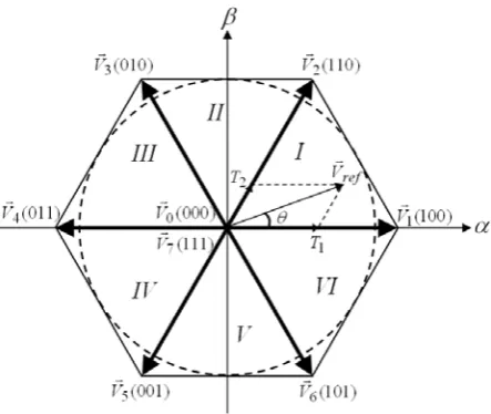
Space vector PWM switching techniques have been widely used in industrial inverter because of their lower current harmonics and higher modulation index [13]. The SVPWM is more suitable to control the shoot-through time in the Z-source inverter. The eight space vectors V0−V7, illustrated in Fig. 4, are used in
SVPWM, where V1−V6 are active vectors, and V0 and
V7 are null vectors. If the reference voltage vector, Vref
is located between the arbitrary vector Vi and Vi+1, the
reference voltage vector is divided into two adjacent voltage vectors (Vi and Vi+1) and null vectors (V0 and
V7). In a sampling interval Ts, voltage vectors Vi and
Vi+1 are applied during T1 and T2, respectively, and the
null vectors are applied during T0=Ts−(T1+T2).
Consequently, the reference voltage vector Vref can be
obtained as follows [14]:
ref 1 i 2 i 1 0 0 7
V =T V T V+ + +T (V or V )
r r r r r
(7)
The time intervals T1 and T2 can be obtained as [15]
ref
1 s
i
V
T 3 ˆ T sin(n )
3 V
π
= − α
r
(8)
ref
2 s
i
V (n 1)
T 3 ˆ T sin( )
3 V
−
= α − π
r
(9)
where α is the angle between the reference voltage vector, Vref and voltage vector V1, and n is the number
of sector in which reference vector is located.
The symmetrical pulse pattern of voltage vectors V1,
V2 and zero vectors V0 and V7 during one sampling
period at the modified space vector PWM is illustrated in Fig. 5. Unlike the traditional SVPWM, the modified SVPWM has an additional shoot-through period Tsh
besides time intervals T1, T2 and T0. The zero voltage
period T0 should be modified for generating the
shoot-through time interval Tsh. The shoot-through time
interval is evenly assigned to each phase with Tsh/6,
which the active state time intervals T1 and T2 are not
changed.
Fig. 4 Basic space vector PWM.
4 Minimization of Voltage Stress across Devices In order to obtain the voltage gain of the modified SVPWM, switching pattern, which is shown in Fig. 5, is used. As it can be seen in this figure, the time interval of the second null vector, V7, is equal to T0/4-2Tsh/6. Since
this interval must be positive and more than zero, therefore the shoot trough interval is limited to 3T0/4.
sh 0
sh 0
s s
s 1 2 1 2
s s
T T
3 3
T T
4 T 4 T
T (T T ) (T T )
3 3 1
4 T 4 T
= ⇒ =
⎛ − + ⎞ ⎛ + ⎞
= ⎜ ⎟= ⎜ − ⎟
⎝ ⎠ ⎝ ⎠
(10)
Using the Eq. (8) and (9), the total time interval of active switching, Ta, in section 1, can be calculated as
bellow:
ref
a 1 2 s
i
V
n 1 T T T 3 ˆ T sin( )
3 V
π
= ⇒ = + = α +
r
(11)
As it can be seen, this active time interval, Ta, varies
during any section of space vectors. This variation is regular during any π/3 interval. Therefore in order to obtain the voltage gain, it is enough to calculate the average of Ta in section 1, between 0 and π/3 [16]:
Fig. 5 Switching pattern for both traditional SVPWM and
modified SVPWM.
ref 3
a avg 0 s
i
ref s
i
V 1
(T ) 3 ˆ T sin( ) d
( 3) V 3
V 3 3T
ˆV
π π
= α + α
π
= π
∫
rr (12)
Since the value of reference voltage, Vref
r is equal to
maximum value of the output phase voltage, hence the average of Ta can be expressed as the following:
ac ac
a avg s s
i i
ˆ ˆ
V V
3 3 3 3
(T ) T ˆ T ˆ
2
V V 2
= =
π π (13)
and then:
ac
a avg s
i
a avg sh
s s
sh s
ˆV 3 3M
M (T ) T
ˆ 2
V 2
(T )
T 3 3 3 3M
1 1
T 4 T 4 2
T 3 2 3 3M
T 4 2
= ⇒ =
π
⎛ ⎞
⎛ ⎞
⇒ = ⎜ − ⎟= ⎜⎜ − π ⎟⎟
⎝ ⎠ ⎝ ⎠
⎛ π − ⎞
⇒ = ⎜⎜ ⎟⎟
π
⎝ ⎠
(14)
where M is the modulation index. The value of boost factor, B, based on the modulation index can be deduced as follows:
sh s
1 4
B
1 (2T T ) 9 3M 2
π
= =
− − π (15)
Therefore the voltage gain, G of the modified SVM can be written as below:
ac dc
ˆV 4 M
G MB
V 2 9 3M 2
π
= = =
− π (16)
Also for given voltage gain, G, the modulation index is:
2 G M
9 3 G 4
π =
− π
(7)
In Fig. 6, the voltage gain of the modified SVM based on the modulation index is shown.
5 Control Algorithm of the DC Boost Voltage The dc-link voltage Vi is a square waveform due to
the shoot-through states. During the non-shoot-through states, the dc-link voltage is in its peak value, ˆVi, and it
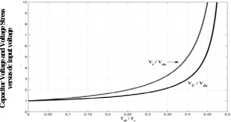
is zero in the shoot-through states. Therefore, the peak value of dc-link voltage is not suitable for using as a feedback signal. Most of the papers have used the Z-source capacitor voltage as a feedback signal, and have controlled the capacitor voltage in a constant value. Regarding to Eq. (5), the capacitor voltage VC is related
to the dc-link voltage of the inverter and can be boosted
by controlling the shoot- through duty ratio. Fig. 7 shows the relationship between VC/Vdc and the
shoot-through time duty ratio Tsh/Ts. As the relationship has
nonlinear characteristics, the shoot-through time cannot linearly control the capacitor voltage. The nonlinearity may deteriorate the transient response of the capacitor voltage. In order to overcome this problem, in this paper an algorithm is used for controlling linearly the capacitor voltage using neural networks controller as shown in Fig. 8. The output of the neural network controller of VC is called K and it can be defined as [13]
C dc
V K
V
= (18)
In order to have VC greater than Vdc, the parameter
K must be greater than 1. Using Eq. (5), the shoot-through period, Tsh can be calculated from the following
equation:
Fig. 6 Relationship between voltage gain and modulation
index, M in modified space vector PWM.
Fig. 7 Relationship between capacitor voltage and voltage
stress and shoot-through duty ratio.
Fig. 8 Capacitor voltage controller using neural network.
Capacitor Voltage and
Voltage Stress
ve
rs
us dc
in
p
ut volta
g
e
( V )
sh s
K 1
T T
2K 1
− =
− (19)
As the capacitor voltage is linearly controlled by K, a good transient performance of capacitor voltage can be obtained.
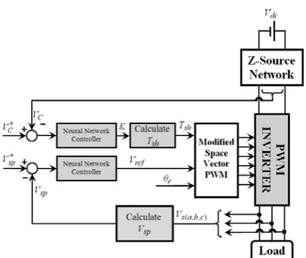
6 Control Algorithm of the AC Output Voltage Figure 9 shows the block diagram of the voltage control of Z-source inverter, which consists in the dc boost voltage control unit, using the linearization method and the ac output voltage control unit. As shown in Fig. 9, the peak value of the output voltage is used to control the ac output voltage. After detecting the three-phase line voltages, the three-three-phase voltages are transformed into two-axis voltages in the stationary reference frame Vds and Vqs, and then the peak output
voltage Vsp can be derived as below [13]:
s 2 s 2
sp ds qs
V = (V ) +(V ) (20)
The output of the neural networks controller (Vsp)
forms the reference voltage for modified SVPWM. The phase angle θe determines the sector in which the
reference voltage vector is located, and six PWM signals are generated from the reference voltage and shoot-through time interval in each sampling period.
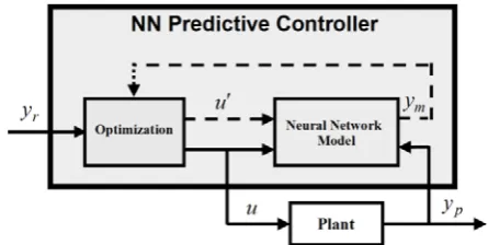
7 Neural Network Controller Design
Neural networks have been applied very successfully in identification and control of many dynamic systems. The universal approximation capabilities of the multilayer perceptron have made it a popular choice for modeling nonlinear systems and for implementing general-purpose nonlinear controllers [17]. In [17] a neural network has been used to determine the parameters KP and KI of a PI controller to
control only the dc boost voltage in wide range. As the inverter’s output voltages are the final outputs of the system, and it is more important to control these outputs, in this paper, two neural network predictive controllers have been used in parallel, to predict and control the both dc boost voltage and ac output voltages of the Z-source inverter.
The proposed neural network predictive controller uses a neural network model of a nonlinear plant to predict future plant performance. The controller then calculates the input signal that will optimize plant performance over a specified future time horizon. The first step in model predictive control is to determine the neural network plant model (system identification). Next, the plant model is used by the controller to predict future performance. The neural network plant model is trained offline, in batch form, using the Back-propagation training algorithms. The controller applies an algorithm, which requires significant amount of
Fig. 9 Block diagram for voltage control of the Z-source
inverter.
online computations, to produce the optimal input signal at each sample time. The following subsection describes the system identification process. Then it is followed by a description of the optimization process [15].
7.1 System Identification
The first stage of model predictive control is to train a neural network to represent the forward dynamics of the plant. The prediction error between the plant output and the neural network output is used as the neural network training signal. The process is represented in Fig. 10. The neural network plant model uses previous inputs and previous plant outputs to predict future values of the plant outputs. The structure of the neural network plant model is given in the Fig. 11. This network has been trained offline in batch mode, using training samples collected during the plant operations. In this paper the Levenberg-Marquardt training algorithm (trainlm) has been used.
As it can be seen in Fig. 11, the neural network has one hidden layer. The number of neurons in the hidden layer of the plant model network for the both dc boost and ac output voltage controllers is equal to 20. The number of the two tapped delay lines coming into the plant model for both inputs and outputs is equal to 2. The sampling Interval at which the program collects data from the Simulink plant model is 1 millisecond. The number of training samples generated for training, validation, and test sets is 10000. The minimum and maximum plant input for the dc boost voltage controller are 1 and 3 and for the ac output voltage controller is 0 and 50 respectively. The random plant input is a series of steps of random height occurring at random intervals. These fields set the minimum and maximum height and interval. The minimum and maximum value of time interval is 0.1 and 0.2 seconds respectively. The number of iterations of plant training to be performed (training epochs) is 100.
Fig. 10 Model predictive control process.
Fig. 11 The structure of the neural network plant model.
7.2 Neural Network Predictive Controller Design The model predictive control method is based on the receding horizon technique [18]. The neural network model predicts the plant response over a specified time horizon. The predictions are used by a numerical optimization program to determine the control signal that minimizes the following performance criterion over the specified horizon.
2
1 u
N
2
r m
j N N
2 j 1
J (y (t j) y (t j))
(u (t j 1) u (t j 2)) =
=
= + − +
′ ′
+ ρ + − − + −
∑
∑
(21)Where N1, N2 and Nu define the horizons over which
the tracking error and the control increments are evaluated. The variable u' is the tentative control signal, yr is the desired response, and ym is the network model
response. The value of ρ determines the contribution that the sum of the squares of the control increments has on the performance index.
Fig. 12 illustrates the neural network controller structure. The controller consists of the neural network plant model and the optimization block. The optimization block determines the values of u' that minimize Jacobian matrix J, and then the optimal u is applied to input of the plant. The Jacobian matrix contains first derivatives of the network errors with respect to the weights and biases. The controller block is implemented in Simulink environment. The cost horizon N1 is fixed at 1. The cost horizon N2 that is the
number of time steps over which the prediction errors are minimized, is equal to 5 and 8 for the dc boost and ac output voltage controllers respectively.
Fig. 12 Neural network predictive controller structure.
The control horizon Nu is fixed to 2 for the both
controllers. The control weighting Factor ρ which multiplies the sum of squared control increments in the performance function is 0.02 and 0.04 for the dc boost and ac output voltage controllers respectively. The parameter α is used to control the optimization. It determines how much reduction in performance is required for a successful optimization step. It is equal to 0.001 for the both controllers. The number of iterations of the optimization algorithm to be performed at each sample time is 2 for the both controllers. Also the linear minimization routine srchbac (backtracking search routine) has been used by the optimization algorithm.
8 Simulation Results
In this part of paper, the values of the inductances and the capacitors of the impedance network are calculated, based on the relations given in section 2. It must be mentioned that the load of the Z-source inverter is a three phases RL with 2 kW nominal power, and power factor of 0.8. Line to line nominal voltage is 400V and the output frequency is set to 50 Hz. Also a 100V dc voltage source supplies the input of the Z-source inverter. The switching frequency of the modified SVPWM is set to 5 kHz. Note that the parameters of the impedance network are calculated for nominal power, but the system is simulated for different conditions. The output nominal current of the Z-source inverter can be calculated as below:
Load Load Load Load
P = 3 V I cosφ ⇒ I =3.6 A (22)
With 400V line to line output voltage, the value of the amplitude of the output voltage is given as the following:
L L ac
V 2 400 2
ˆV 326.6 V
3 3
−
= = = (23)
Therefore by using the modified SVPWM, the value of voltage gain, G, of the Z-source inverter becomes:
ac dc
ˆV 4 M
G MB 6.53
V 2 9 3M 2
π
= = = =
− π (24)
Thus the value for modulation index, M for this switching method is equal to 0.46.
Using Eq. (14), the value of nominal ratio of shoot-trough can be written as below:
sh sh
s
T 3 2 3 3M
D 0.4646
T 4 2
⎛ π − ⎞
= = ⎜⎜ ⎟⎟=
π
⎝ ⎠ (25)
Using this shoot-trough duty ratio, the mean value of capacitor voltage can be calculated as the following:
sh s
C dc
sh s
1 (T T )
V V 756 V
1 (2 T T )
−
= =
− (26)
Also by using Eq. (1), the mean value for inductance current can be deduced as below:
Load Load Load
L
dc dc
S 3 V I
I 25 A
V V
= = = (27)
By using Eq. (4) and considering a maximum of 10% ripple for inductance current, the value of inductances in Z network can be taken out as the following:
sh C
s L
D V 0.4646 756
L L 1.4 mH
2f I 2 5000 (0.1 25)
×
≥ = ⇒ ≥
Δ × × × (28)
Also by using Eq. (6) and considering a maximum of 1% ripple for capacitor voltage, the value of capacitors in Z-source network can be calculated as below:
sh L
s C
D I 0.4646 25
C
2f V 2 5000 (0.01 756) C 153 F
×
≥ =
Δ × × ×
⇒ ≥ μ
(29)
The calculated values for the inductances and capacitances are the minimum values. In order to have fewer ripples, two 2 mH inductances and two 470 μF capacitors are selected for Z-source network.
Fig. 13 shows the transient response of the value of line to line peak voltage of the Z source inverter output using PI controllers. As can be seen from Fig. 13, the voltage Vsp arrives to its reference, 200V, in 0.2 second.
The transient response of the capacitor voltage using PI controllers has been shown in Fig. 14. As it is shown, this voltage arrives to 236 V after 0.5 second and follows its reference.
Fig. 15 shows the transient response of the value of line to line peak voltage of the Z source inverter output. As discussed before, a predictive neural network controller is used. As it is shown, the voltage Vsp arrives
to its reference, 200V, in less than 0.05 second, and follows it very well. A filtered line to line output voltage of the Z-source inverter is presented in Fig. 16. As it can be seen, the maximum value of line to line output voltage is equal to 200 V. One of the capacitor voltages is shown in Fig. 17. This voltage arrives to 236 V after 0.2 second and follows its reference very well.
Fig. 13 Peak ac line to line output voltage response using PI
controller.
Fig. 14 Z-source network capacitor voltage response using PI
controller.
Fig. 15 Peak ac line to line output voltage response using neural
network controller.
Fig. 16 line to line output voltage response using neural
network controller.
During the shoot-trough states the inverter switches have a zero voltage. During active states, the value of applied dc voltage to the inverter switches ˆVi can be
calculated as the following:
( V )
( V )
( V )
Fig. 17 Z-source network capacitor voltage response using
neural network controller.
Fig. 18 line to line switched voltage of Z-source inverter.
i dc
sh s
1
ˆV V
1 (2T T ) 1
100 357 V 1 (2 0.35)
= ×
−
= × =
− ×
(30)
The line to line switched voltage of Z-source inverter is given in Fig. 18. It can be observed that the instantaneous amplitude arrives to 360 V.
Figure 19 shows the variation of the peak value of line to line output voltage using PI controllers when the reference value of V*
sp varies from 180 V to 250 V.
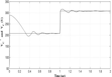
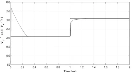
The variation of the capacitor voltage in order to provide the considering output voltage using PI controllers has been shown in Fig. 20. Fig. 21 shows the variation of the peak value of line to line output voltage when the reference value of V*
sp varies from 180 V to
250 V. Also the variation of line to line output voltage from 180 V to 250 V is shown in Fig. 22. One of the capacitor voltages is presented in Fig. 23. In order to provide the output voltage, this voltage varies from 208 V to 308 V.
9 Conclusion
In this paper, structure, equivalent circuit and main equations of a Z-source inverter are studied. The dc-link voltage and the ac output voltages are controlled simultaneously. At first stage, in order to have a good performance, the values of inductances and capacitors
are calculated by linearization of the inductances currents and capacitors voltages. Then a modified space vector PWM is presented to perform the inverter switching. Since the peak value of dc-link voltage is related to capacitors voltages, by controlling the capacitor voltages, the control of dc-link voltage is performed. Also, the shoot-through ratios are determined by this linearization of the capacitor voltage control. Moreover, in this paper, the peak value of the line to line ac output voltage is controlled by using a modified switching algorithm. This algorithm lets to minimize the dc voltage stress across the inverter switches. As it is shown by simulation, PI controllers cannot offer good performances; in this paper two predictive neural network controllers are applied to ameliorate the dynamic performance of simultaneous control of dc boost voltage and ac output voltages. Simulation results show a higher performance, rapid response and fewer ripples in both input and output sides of inverter.
Fig. 19 variation of the peak value of line to line output
voltage from 180 V to 250 V using PI controller.
Fig. 20 Variation of capacitor voltages from 208 V to 308 V
using PI controller.
( V )
( V )
( V )
( V )
Fig. 21 variation of the peak value of line to line output
voltage from 180 V to 250 V using NN controller.
Fig. 22 Variation of the line to line ac output voltage from 180
V to 250 V using NN controller.
Fig. 23 Variation of capacitor voltages from 208 V to 308 V using
NN controller.
References
[1] Gajanayake J., Vilathgamuwa D. M. and Loh P. C., "Small-Signal and Signal-Flow-Graph Modeling of Switched Z-Source Impedance Network", IEEE Power Electron. Letters, Vol. 3, No. 3, pp. 111-116, Sept. 2005.
[2] Nemati A. and Pakdel M., "A New ZVZCS Isolated Dual Series Resonant DC-DC Converter with EMC Considerations", Iranian Journal of Electrical & Electronic Engineering (IJEEE), Vol. 6, No. 3, pp 190-198, Sept. 2010.
[3] Peng F. Z., "Z-source inverter", IEEE Trans. Ind. Appl., Vol. 39, No. 2, pp. 504-510, Mar./Apr. 2003.
[4] Dehghan S. M., Mohamadian M., Yazdain A., Rajaei A. H. and Zahedi H., "Dual Z-Source Network Dual-Input Dual-Output Inverter", Iranian Journal of Electrical & Electronic Engineering (IJEEE), Vol. 6, No. 4, pp. 205-213, Dec. 2010.
[5] Peng F. Z., Joseph A., Wang J., Shen M., Chen L., Pan Z. and Huang Y., "Z-Source inverter for motor drives", IEEE Trans. Power Electron., Vol. 20, No. 4, pp. 857-863, July 2005.
[6] Rostami H., Khaburi D. A., "Voltage gain comparison of different control methods of the Z-source inverter", International Conf. on Electrical and Electronics Engineering, ELECO, pp. 268-272, Nov. 2009.
[7] Thangaprakash S. and Krishnan A.,
"Implementation and Critical Investigation on Modulation Schemes of Three Phase Impedance Source Inverter", Iranian Journal of Electrical & Electronic Engineering (IJEEE), Vol. 6, No. 2, pp 84-92, June 2010.
[8] Peng F. Z., Shen M. and Qian Z., "Maximum boost control of the Z-source inverter", IEEE Trans. Power Electron., Vol. 20, No. 4, pp. 833-838, July 2005.
[9] Shen M., Wang J., Joseph A., Peng F. Z., Tolbert L. M. and Adams D. J., "Maximum constant boost control of the Z-source inverter", IEEE/IAS, pp. 142-147, Seattle 2004.
[10] Rajakaruna S. and Jayawickrama Y. R. L., "Designing impedance network of Z-Source inverters", IEEE Power Engineering Conf., pp. 1-6, Nov. 2005.
[11] Rabkowski J., "The bidirectional Z-source inverter for energy storage application", European Conference on Power Electronics and Applications, pp. 1-10, 2007.
[12] Shen M., Joseph A., Huang Y., Peng F. Z. and Qian Z., "Design and development of a 50 kW Z-source inverter for fuel cell vehicles", in Proc. Int. Conf. Power Electron. Motion Control, pp. 1076-1080, Shanghai, China, 2006.
[13] Tran Q. V., Chun T. W., Ahn J. R. and Lee H. H., "Algorithms for Controlling Both the DC Boost and AC Output Voltage of Z-Source Inverter", IEEE Trans. Indust. Electron., Vol. 54, No. 5, pp. 2745-2750, Oct. 2007.
[14] Chun T. W., Tran Q. V., Ahn J. R. and Lai J. S., "AC Output Voltage Control with Minimization of Voltage Stress Across Devices in the Z-Source Inverter using Modified SVPWM", IEEE APEC, pp. 1-5, 2008.
[15] Rostami H., Khaburi D. A., "Neural networks controlling for both the DC boost and AC output voltage of Z-source inverter", 1st Power Electronic and Drive Systems and Technologies Conf., pp. 135-140, Feb. 2010.
( V )
( V )
[16] Rostam minim source System [17] Fatemi M. J. R Z-sour Conf. ICEMS [18] Solow Predic IEEE Contro
mi H., Khabu mizing of volta e inverter", 2n ms and Techno i M. J. R., M R., "Wide-ran rce inverter b on Electric MS 2008, pp. 16 way D. and Ha tive Control"
Internationa ol, pp. 277-28
uri D. A., "A age stress acro d Power Elec ologies Conf., Mirzakuchaki S
nge control of by neural netw cal Machines
653-1658, 200 aley P. J., "Ne ", Proceeding
l Symposium 1, 1996.
new method oss devices in ctronic and Dr
Feb. 2011. S. and Fatem
output voltag work", IEEE s and Syste 08.
eural Generali gs of the 19 m on Intellig
for n Z-rive mi S. e in Int. ems, ized 996 gent Un me Au Ele 201 Eng Kh con ele DS
niversity of Sci mber of Cen utomation and O
ectronic and Mo
10, he has b gineering, Kha hameneh, Iran. nverters and m
ctronics and e SPs.
Davood A
1965. He from Sharif Electronic Ph.D. from France in 1 He has joi France (199 been as a ience & Techn nter Of Exce
Operation. His otor Control.
Hamid Ro
Iran, in 1 degree in Engineerin University 2007 and t Engineerin University (IUST), T been with the ameneh Branch . His researc motor drivers a electric drives
Arab Khaburi
has received B f University of
Engineering a m ENSEM IN
1994 and 1998 ined to UTC i 98-1999). Sinc a faculty mem nology (IUST) ellence for Po
research inter
ostami was b
1983. He rece n Electrical a ng Departmen of Tabriz, T the M.S. degre ng Departmen of Science an Tehran, Iran in e Department h, Islamic Az ch interests i as well as con
using microc
was born in B.Sc. in 1990 Technology in and M.Sc. and NPEL, Nancy, 8, respectively. in Compiegne, ce 2000 he has mber of Iran . He is also a ower Systems ests are Power
orn in Tabriz, eived the B.S. and Computer nt from the Tabriz, Iran in ee in Electrical nt from Iran nd Technology n 2010. Since of Electrical zad University, include power ntrol of power controllers and n 0 n d , . , s n a s r , . r e n l n y e l , r r d