Creative Components Iowa State University Capstones, Theses and Dissertations
Spring 2018
New Memory Technologies
New Memory Technologies
Nishtha Bhatnagar
Iowa State University, [email protected]
Follow this and additional works at: https://lib.dr.iastate.edu/creativecomponents
Part of the Engineering Commons
Recommended Citation Recommended Citation
Bhatnagar, Nishtha, "New Memory Technologies" (2018). Creative Components. 139. https://lib.dr.iastate.edu/creativecomponents/139
New Memory Technologies
By
Nishtha Bhatnagar
A creative component report submitted to the graduate faculty in partial fulfillment of the requirements for the degree of
MASTER OF SCIENCE
Major: Electrical Engineering
Program of Study Committee: Prof. Vikram Dalal, Major Professor Prof. Long Que, Co-Major Professor
Iowa State University Ames, Iowa
Contents
List of Figures ... 3
List of Tables ... 4
Acknowledgement ... 5
Abstract ... 6
Chapter 1. Introduction ... 7
Memory ... 7
Volatile Memory ... 7
Non-Volatile Memory: ... 7
Chapter 2. Background Information ... 8
Overview of Different types of Memory ... 8
2.1 SRAM (Static Random-Access Memory) ... 8
2.2 DRAM Memory (Dynamic Random-Access Memory) ... 9
2.3 Flash Memory ... 10
2.4 3DXP Memory ... 13
Chapter 3. Work as 3DXP Engineer ... 15
Work on 3DXP Memory ... 15
Chapter 4: Projects and Discussion on 3DXP Memory ... 16
4.1 3DXP Training ... 16
4.2 Special Work Request (SWR) Analysis ... 16
Chapter 5. Conclusion ... 19
List of Figures
Figure 1. 1 Memory Classification ... 7
Figure 2. 1 SRAM Memory Cell ... 8
Figure 2. 2 Cross-coupled inverters ... 8
Figure 2. 3 Write operation ... 9
Figure 2. 4 DRAM Memory Cell ... 9
Figure 2. 5 Floating Gate MOSFET... 10
Figure 2. 6 Floating Gate Charge States in Logic 0 and 1 ... 10
Figure 2. 7 Read Operation... 11
Figure 2. 8 Quantum Tunneling ... 11
Figure 2. 9 Hot Electron Injection Effect ... 11
Figure 2. 10 Erase Operation ... 12
Figure 2. 11 NOR Flash ... 12
Figure 2. 12 NAND Flash ... 12
Figure 2. 13 Memory Trend... 13
Figure 2. 14 3DXP Memory Architecture ... 13
Figure 3. 1 Micron Internship Timeline ... 15
Figure 4. 1 Number of dies failing in a wafer seen in ESDA software ... 16
Figure 4. 2 Underexposure causing shorts ... 17
Figure 4. 3 Underexposure led to WL-WL shorts which led to selecting two memory cells .. 17
List of Tables
Acknowledgement
• I would like to express my gratitude to Prof. Vikram Dalal for always showing me the right path and supporting me throughout my journey. The work in Dr Dalal’s Lab helped me to understand more about fabrication of solar cells, learn about measurements like IV and QE measurements. Also it helped me to present data by a particular deadline and exposed me to work under pressure which further helped me at Micron Technology
• My thanks to Prof. Long Que who provided me feedback and gave me valuable suggestions. I was first introduced to data during my summer work in Dr Que’s lab where I was working on Brain Cells where I had to keep a track of number of regenerating bran cells. This acquired knowledge helped me to solve problems at industrial level
• Big thanks to Micron Technology for providing me this great opportunity that helped me to grow as a person. I was exposed to an industrial environment where I worked upon my weaknesses and strengthened the abilities I already possessed
• Micron Manager Mrs. Marsela Pontoh for being a great supervisor • Team Members at Micron for their guidance and support
Abstract
Memory is used to store the data. Semiconductor memory can be used as our computer’s cache memory, in our mobile applications, in memory cards of our cameras.
To meet the growing needs for memory, variety of different memories are used like DRAM, SRAM, etc. With the rapid growth in the requirement of memories new memory technologies are being developed and considerable amount of research is invested in these new memory technologies. One of a very new memory technology is 3DXP Memory. 3DXP is a type of Non-Volatile memory which has very high density and high speed as compared to any other Non-Volatile memory. It can be used in various applications like Genomics, sensing. In this report, I would like to introduce 3DXP Memory development and my work as a 3DXP Yield Enhancement Electrical Failure Analysis Engineer.
Chapter 1. Introduction
Memory
Memory is a Physical device which stores data on permanent or temporary basis. It is just like a human brain which stores all the information. From the clicked pictures in our cameras to the text messages in a mobile phone, memory is needed everywhere. It contains a circuit that stores large array of digital information.
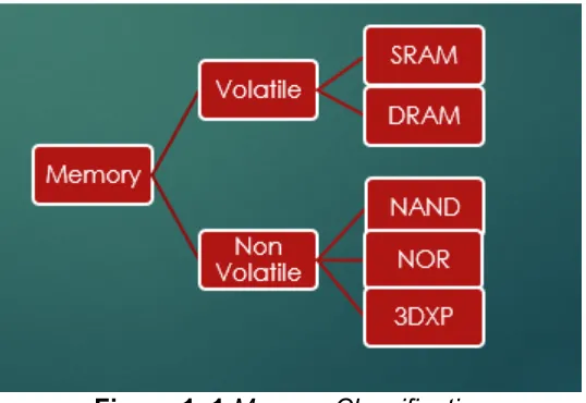
Memory can be classified into below categories:
Figure 1. 1 Memory Classification
Volatile Memory
This type of memory[1] requires power to retain the data. It loses its content as soon as power is turned off.
Examples: SRAM memory, DRAM memory Usage: It is used in computer’s main memory
Non-Volatile Memory:
This memory stores the information even if the power is turned off. It can permanently store the information.
Examples: NAND Flash, NOR Flash, 3DXP Memory Usage: It is used in Laptops, Tablets, MP3 player, phones
[image:8.595.164.433.217.402.2]Chapter 2. Background Information
Overview of Different types of Memory
2.1 SRAM (Static Random-Access Memory)
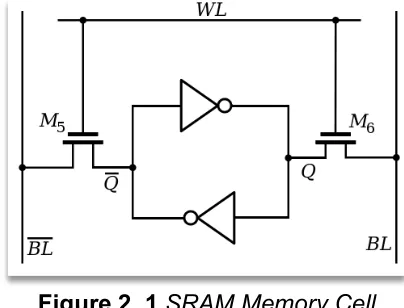
SRAM Memory[4] is a class of Volatile Memory which has very fast Read and Write operations. It is widely used in Cache Memory.
Construction
Figure 2. 1 SRAM Memory Cell
It consists of two cross coupled inverters i.e. four transistors to store each bit of data. Also, there are two access transistors (here M5 and M6) which are used to control the access to the storage cell during Read and Write operations. As it contains 6 transistors to store a bit, its structure is complex, and it consumes more power.
Working
Figure 2. 2 Cross-coupled inverters
Retaining:
Cross coupled inverters act like a feedback loop and help in retaining the data.
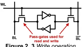
Writing:
We have to give a high voltage on the WL, so that the MOSFET switches close and provide access to the memory cell. BL and BL_Bar will act like an input.
[image:9.595.194.396.229.383.2]Figure 2. 3 Write operation
Reading:
The bit-line is pre-charged to Vdd/2 and WL is at a high voltage. If the memory cell has logic 0 stored in it, the BL will go low and BL_Bar will go high. Hence, the difference would be negative which would be sensed by a sense amplifier.
If Logic 1 is stored, then BL will go high and BL_Bar will go low. Hence, the difference would be positive.
Memory cell BL BL_bar Difference
0 Low High Negative
[image:10.595.214.383.70.167.2]1 High Low Positive
Table 2. 1 Read Operation
2.2 DRAM Memory (Dynamic Random-Access Memory)
DRAM Memory[7] is also a Volatile Memory and is cheaper than SRAM. It is used in computer’s Main Memory, PDAs, game machines, digital audio devices, et cetera.
Construction
Figure 2. 4 DRAM Memory Cell
Each memory cell has a capacitor and an access transistor. Data is stored in DRAM as charge on a capacitor.
Capacitor is either charged to full Vdd level (Logic 1) or ground (Logic 0).[3]
[image:10.595.72.498.280.358.2] [image:10.595.216.380.478.617.2]Working
Writing:
WL remains high to close transistor switch. If we want to write Logic 1, we will give high voltage to BL. If we want to write Logic 0, then we will connect BL to ground.
Reading:
We can read what’s stored in DRAM Memory by turning the access transistor ON and this output goes into the BL which will further go into the sense amplifier. If the sensed voltage is more than the reference value (Vdd/2) then it is as considered Logic 1 else, it is Logic 0.
2.3 Flash Memory
Flash Memory is a Non-Volatile memory which has very high density. It is used in SSDs, Memory sticks, cameras. It uses the concept of floating gate MOSFETs.
Construction
Figure 2. 5 Floating Gate MOSFET
It uses floating gate MOSFET[8] to store data. It consists of two gates, 1) a floating gate which is electrically isolated and not connected to any metal contacts, 2) a control gate which is connected to the gate terminal.
The two gates are separated by a thick oxide layer called as an Inter-Poly Dielectric or a Blocking Oxide and the other oxide layer is called as a Tunnel Oxide.
Working
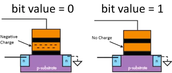
Reading:
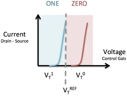
[image:11.595.201.395.326.448.2] [image:11.595.156.434.597.716.2]Figure 2. 7 Read Operation
Value 0 will have higher threshold voltage than value 1 due to accumulation of negative charges on the floating gate.
We will give a voltage between threshold voltage of logic 0 and threshold voltage of logic 1 and will measure the current. If there is no current, then it’s a logic 0 else a Logic 1.
Programming:
Figure 2. 8 Quantum Tunneling
NAND Memory uses Quantum Tunneling [5] mechanism for programming. When high negative voltage is applied on the control gate the barrier shape changes. The electrons in the channel see a triangular barrier which is easy to pass than rectangular barrier. The electrons move from channel into the floating gate.
Figure 2. 9 Hot Electron Injection Effect
[image:12.595.194.401.84.246.2] [image:12.595.221.376.377.475.2] [image:12.595.211.391.558.647.2]Erasing:
Figure 2. 10 Erase Operation
Erase operation in both NAND and NOR can be done by Quantum Tunneling mechanism. When high positive voltage is applied to the control gate, the electrons in the floating gate cross the barrier goes and go into the p substrate.
[image:13.595.180.419.280.385.2]NOR Flash Structure:
Figure 2. 11 NOR Flash
Read
We will apply an intermediate voltage (between threshold of Logic 1 and 0) to the cell we want to read and low voltages to all other floating gate MOSFETs to make sure they do not conduct.
Program (Logic 0): High voltage is given to the drain and a gate voltage greater than threshold voltage to the memory cell we want to program.
Erase (Logic 1): High negative gate voltage is applied, and value of all floating gate cells are set to 1 by quantum tunneling mechanism.
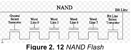
[image:13.595.183.414.585.673.2]NAND Flash Structure:
Figure 2. 12 NAND Flash
Read
Program (0): High positive gate voltage is applied to the memory cell we want to program in order to program it through quantum tunneling.
Erase (1): High negative gate voltage is applied, and value of all floating gate cells are set to 1 by quantum tunneling mechanism.
[image:14.595.152.447.183.304.2]2.4 3DXP Memory
Figure 2. 13 Memory Trend
New revolutionary Non-Volatile memory after 36 years with improved performance. It was announced in 2015 and is a joint venture of Intel and Micron. The production is in Lehi, Utah.
It’s a faster, transistor-less, stackable and inexpensive memory. It is not limited by number of programs cycles hence, has high endurance. It also has high density and low latency as compared to NAND. [3]
It can be used in variety of applications such as Gaming, Pattern recognition and Genomics.
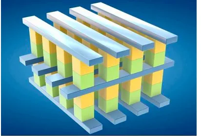
3DXP Architecture
Figure 2. 14 3DXP Memory Architecture
This memory uses cross-point array architecture, perpendicular BL and WL connect submicroscopic columns.
It consists of memory cell which stores single bit data and a selector which enables memory cell to be written or read without using a transistor.
[image:14.595.196.402.460.600.2]Working
Each memory cell can be individually addressed by selecting its top and bottom line, i.e. BL and WL. [2]
It uses phase change material with different resistances for storing data. Amorphous state to store logic 0 and crystalline state to store logic 1. Selector device is used to access the device.
It consumes very less power than NAND and has more write/read speeds than any non- volatile memory.
[image:15.595.80.521.237.496.2]Summary
Chapter 3. Work as 3DXP Engineer
Work on 3DXP Memory
Worked as Yield Enhancement Electrical Failure Analysis Engineer. Interacted with Process Integration, process, probe and product engineers. Analyzed probe, parametric and fab data to identify yield issues. Published and presented reports on analysis in meetings. Applied knowledge of silicon fabrication steps to identify and troubleshoot yield issues. [2]
Figure 3. 1 Micron Internship Timeline
Responsibilities included to identify interactions between process modules and equipment to detect fail mechanisms. I was also responsible to monitor the end of line performance to identify unexpected shift.
[image:16.595.120.475.219.355.2]Chapter 4: Projects and Discussion on 3DXP Memory
4.1 3DXP Training
Project Goal:
Project aim was to gain basic understanding of 3DXP-20 series working and 3DXP architecture and to complete online trainings on SPC, Statistics, JMP and Yield3 training.
Introduction to YE Tools like Unix, Putty, Micron central, Data Daemon.
Outcomes:
After undergoing some trainings, I was able to extract probe data from Yield3 and I analyzed data using JMP. I performed probe to inline correlation and simple data mining like good vs bad analysis. I also supported few SWRs which helped in applying data extraction techniques, preparation and process knowledge and used them to make analysis.
4.2 Special Work Request (SWR) Analysis
Project Goals:
Goal for this project was to complete SWR Analysis using YE tools by deadline. Also, had to
interact with respective process owners and learn, understand the particular process like Lithography, Etching. Aim was to present conclusive solutions in the weekly meetings.
Outcomes:
Figure 4. 1 Number of dies failing in a wafer seen in ESDA software
Green: Good Dies
Orange: Bad Dies
I got exposed to interact with SWR owner and PI Engineer from both R&D and manufacturing fabs. I was given opportunity to focus on small portion of the process flow and analyze how changes in particular process can affect electrical metric. I used ESDA (Enhanced software for data analysis) to map the failing bins in a wafer. Example- Worldline fails due to short circuits identified by particular pattern on map. I also presented analysis and gave recommendations to the process owners.
Process:
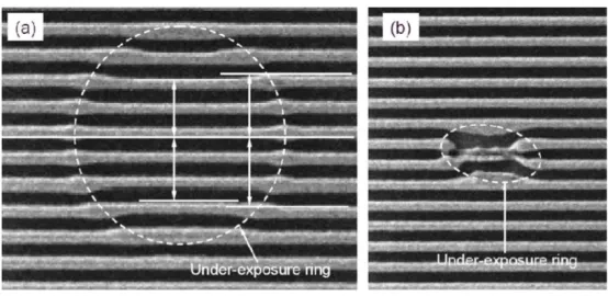
group wafers where new process was introduced. I had to extract the process data from Yield3 and analyze the data in JMP. I had to check for any toggles in comparison with other control group wafers. Final step was to electrically analyze the data and find the causes about the failing dies. Main goal was to find the size and shap4e of the defect, density of defect, defect location and causes of defect.
Figure 4. 2 Underexposure causing shorts
Example: Word-line-Word-line shorts caused due to under exposure during Lithography.
Figure 4. 3 Underexposure led to WL-WL shorts which led to selecting two memory cells
4.3 Weekly Trend Analysis
Project Goals:
To Perform probe trend analysis and highlight shift needs to be followed up and to present outcomes in weekly group meetings.
Outcomes:
In this project I worked on weekly tracking of defined set of critical yield metric and flagged unexpected trend seen like more fails due to new reticle mask change, I also checked for potential shift cause and performed correlations. I was exposed to JMP Scripting Language and I also automated Weekly trends analysis. I was also able to highlight fails and worked on follow up items.
Process:
[image:18.595.157.434.153.288.2] [image:18.595.200.400.355.496.2]and the trend’s direction. I could focus more on the top metrics rather than visually seeing all 600 metrics.
Example:
[image:19.595.168.433.116.210.2]Chapter 5. Conclusion
The main aim was to do a literature survey on all existing memories and to work on 3DXP Memory at Micron Technology.
After reviewing the literature and working as 3DXP YE Engineer I can say 3DXP is a very promising Non Volatile memory which is 1000X times faster than NAND Memory [2]. It also has 10X more density than DRAM. It has low cost and low latency in nanoseconds as compared to NAND which is in microseconds. The lifetime is also not impacted by number of write cycles. 10 series has dual decks and 20 series have quad decks with higher densities.
During my internship I was able to produce yield reports to increase yield and find the causes of the fails. I was also able to automate Weekly Trends so that just by a click engineers could see which electric metrics are failing for the particular week and their respective causes. This helped in making the weekly trends analysis more effective.
References
[1] Neil E. Weste, Davis M. Harris,” CMOS VLSI Design: A Circuits and Systems Perspective”
2010, Pearson,4th Edition
[2] Intel-Micron’s Webcast, Link:
https://www.youtube.com/watch?time_continue=1&v=VsioS35D-HY [3] Micron’s Website, Link:
https://www.micron.com [4] SRAM Memory, Link:
https://whatis.techtarget.com/definition/SRAM-static-random-access-memory [5] Ben Streetman, Sanjay Banerjee, “Solid State Electronic Devices”,2014, Pearson,7th
Edition
[7] DRAM Memory, Link:
https://searchstorage.techtarget.com/definition/DRAM [8] Flash Memory, Link: