Detection of Bare PCB Defects by Image
Subtraction Method using Machine Vision
Nadaf F.B.1, V.S.Kolkure.2
P.G. Student, Department of Electronics Engineering B.I.G.C College of Engineering Kegaon, Solapur, India1
Associate Professor, Department of Electronics Engineering B.I.G.C College of Engineering Kegaon, Solapur, India2
ABSTRACT:A Printed Circuit Board (PCB) consists of circuit with electronic components mounted on surface. There are threemain steps involved in manufacturing process, where the inspection of PCB is necessary to reduce the defects. First step is printing, second step is the components fabrication over the PCB surface and third is the components soldering. In this paper Machine Vision PCB Inspection System is applied at the first step of manufacturing, i.e., the making of bare PCB. We first compare a standard PCB image with a PCB image to be inspected, using a simple subtraction algorithm that can detect the defected regions. Our focus is to detect defects on printed circuit boards. Typical defects that can be detected are over etchings (opens), under-etchings (shorts), holes etc.
KEYWORDS:Machine vision, PCB defects, Image subtraction, PCB inspection, Particle analysis
I.INTRODUCTION
NOWADAYS Machine Vision inspection process [1], [2] is necessary to improve the quality of PCB. In manufacturing industry there are defects, misalignment, and orientation error so automated inspection [3], [4] is required. The defects can be analyzed by machine vision using algorithms developed for it. So machine vision provides a measurement technique for regularity and accuracy in the inspection process.
These systems have advantage over human inspection in which subjectivity, fatigue, slowness and high cost is involved. In recent years, the PCB industries require automation due to many reasons. The most important one is the technological advances in
PCB‟s design and manufacturing. New electronic component fabrication technologies require efficient PCB design and
inspection method with compact dimension [5]. The complex and compact design causes difficulties to human inspection process. Another important factor is necessity to reduce the inspection duration. These factors lead to automation in PCB industry. Nowadays automated systems are preferred in manufacturing industry for higher productivity.
II.MATERIAL AND METHODS
A. MACHINE VISION
On a technical ground, it is necessary to implement the proposed theory and method to construct a machine vision system. Machine vision can be implemented for the system involving following processes.
– Automated Inspection process
– Process control
– Data base collection and indexing
– Modeling of system and environment
B. BARE PCB DEFECTS
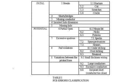
During the manufacturing there are some defects commonly found on PCB. These defects are divided into two categories, potential and fatal defects. Short-circuit and open-circuit defects are in fatal defects category. Breakout, under etch, missing hole, and wrong size hole fall in potential defects category [6], [7], [8]. Fatal defects are those in which the PCB does not meet the objective for which it is designed, while the potential defects are those which compromise the PCB performance during utilization. During etching process, the anomalies occurring on bare PCB could be largely classified in two categories: the one is excessive copper and missing copper. The incomplete etching process leaves unwanted conductive materials and forms defects like short-circuit, extra hole, protrusion, island, and small space. Excessive etching leads to open-circuit and thin pattern on PCB [7], [8]. In addition, some other defects may exist on bare PCB, i.e. missing holes, scratch, and cracks.
There are many ways to designate PCB errors as shown in Table I.
FATAL 1 Breaks 1.1 Fracture 1.2 Cut 1.3 Scratches 1.4 Cracks 2 Shorts/bridges
3 Missing conductor 4 Incorrect hole dimension 5 Missing hole
POTENTIAL 6 Partial Open 6.1 Mouse bit 6.2 Nicks 6.3 Pinholes 7 Excessive spurious 7.1 Specks
7.2 Spurs/protrusions 7.3 Smears 8 Pad violations 8.1 Under etching
8.2 Over etching 8.3 Breakout 9 Variations between the 9.1 Small thickness wiring
printed lines
9.2 Large conductors 9.3 Excessive conductors 9.4 Incipient short
(conductor too close) TABLE I
PCB ERRORS CLASSIFICATION
from one occurrence to another.
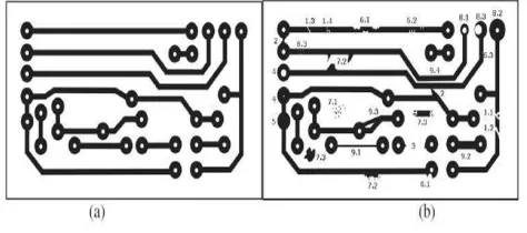
Fig.1 PCB without error (a) PCB with error (b)
C. CONCEPTS OF LOGIC OPERATOR FOR IMAGE
An arithmetic or logic operation between images is a pixel-by-pixel transformation. It produces an image in which each pixel derives its value from the value of pixels with the same coordinates in other images [9].
If A and B are the images with a resolution XY, and Op is the operator, then the image N resulting from the combination of A and B through the operator Op (fig.2) is such that each pixel P of the resulting image N is assigned the value
pn= (pa)(Op)(pb) ; where pa is the value of pixel P in image A, andpbis the value of pixel P in image B.
Fig. 2 Operator Concept
D. LOGIC AND COMPARISON OPERATORS
Logic operators are bitwise operators listed in Table II. They manipulate gray-level values coded on one byte at the bit
level[9]. In the case of images with 8-bit resolution, logic operators are mainly designed to combine gray- level images with mask images composed of pixels equal to 0 or 255 (in binary format 0 is represented as 00000000, and 255 is represented as 11111111), or to combine or compare images with a binary or labeled content (after thresholding the image).
Logical Operators Operator Equation
AND pn = pa AND pb
NAND pn = pa NAND pb
OR pn = pa OR pb
NOR pn = pa NOR pb
XOR pn = pa XOR pb
Logic Difference pn = pa AND (NOT pb)
III. IMPLEMENTATION OF METHOD
To implement the image subtraction logic some software tools are required. There are various tools available for implementation. Here NI Vision Assistant is being used as a development tool.
A. VISION ASSISTANT 2009
Vision Assistant is a tool for prototyping and testing image processing applications. Build custom algorithms with the Vision Assistant scripting feature [9] are used to prototype an image processing application. The scripting feature records every step of the processing algorithm. After completing the algorithm, we can test it on other images to make sure it works. The algorithm is recorded in a Builder file, which is an ASCII text file that lists the processing functions and relevant parameters for an algorithm that we prototype in Vision Assistant.
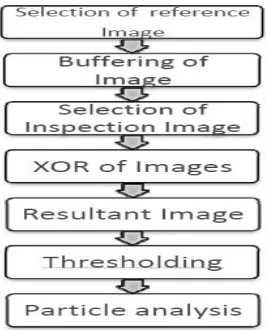
B. INSPECTION FLOW CHART
The PCB inspection using Image subtraction method [7], [10], [11] is performed in steps. As shown in flow chart (fig. 3) the first step load a reference image, second step buffers the reference image so that it can be used for subtraction operation. The third step loads the image which is going to be inspected. To find the PCB error, inspected image is XORed with reference image; this process is also called Image subtraction.
I
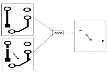
C. IMAGE SUBTRACTION OPERATION
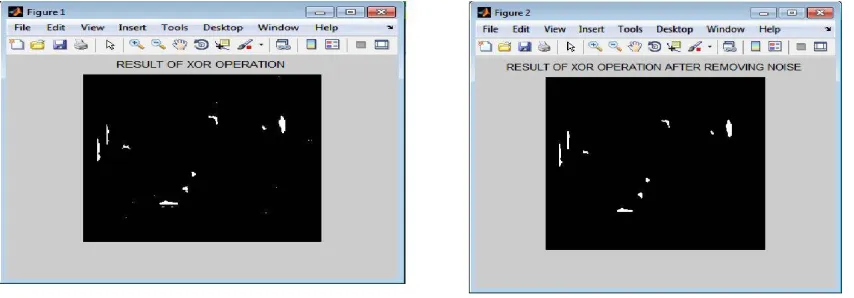
Image subtraction operation is performed in order to get the differences between two images [3], [4]. The images are the reference image and the inspected image. The method compares both images pixel-by-pixel using XOR logic operator [7], [9], [12]. The resulting image obtained after this operation contains defects (fig.4).
The subtraction operation will produce either negative or positive image, „1‟ represents white pixel and „0‟ represents
black pixel in a binary image.
Two rules exists for image subtraction operation Rule 1: If 1-0 = 1 then it gives positive pixel image Rule 2: If 0-1 = -1 then it gives negative pixel image
Fig.4 Image subtraction operation
In fig. 5 and 6, corresponding reference and inspected PCB images are shown. These images are converted into grayscale and added into image buffer before subtraction process. The conversion of image into grayscale is needed for obtaining binary image and this image is further processed for measurement purposes.
Fig. 5 Reference image Fig.6 Image for inspection: - Missing holes
operation gives defects in inspected image as compared with reference image. Fig.7 shows the resultant image and also some other steps are shown in same image which are required in order to perform image subtraction
These steps are shown in icon form.
The resultant image is further processed for thresholding as shown in fig. 8 in order to convert the resultant image in binary form. The binary form of image shows the resultant area into „1‟and „0‟ form. The image area which contains
in formation is represented by „1‟ and rest of portion is considered as‟0‟.
Fig.7 Resultant image after subtraction operation Fig.8 Resultant image after thresholding
Fig 9 and fig 10, represent undertch and final result of the test image.
The above discussed methods namely Image subtraction, and Image Thresholding are repeated for other defects. – Small size and missing holes
-Over Etching -Short conductor
V. CONCLUSION
The bare PCB is analyzed and the defects of PCB are extracted in terms of various parameters. These parameters can be taken as referential data base for further analysis to fabricate defect free PCB and can assist in making an automated system for inspection. In order to use this method in an industrial application some improvements need to be done. Future work consists of inspecting and analyzing a PCB with Surface Mounted Devices.
REFERENCES
[1] Der-BaauPerng, Chuan-Pei Liu, Yen-Chung Chen, and Cheng-Chuan Chou,Advanced SmdPcb Vision Inspection Machine Development Department of Industrial Engineering and Management National Chiao-Tung University, 15th IPPR Conference on Computer Vision, Graphics and Image Processing, 2002
[2] Yi L et al "Machine Vision Algorithms Using Interactive Learning For VFD Inspection," Journal of Applied Intelligence, 2000 [3] Y. Sun, C Tsai. “A New Model-Based Approach for Industrial Visual Inspection”, Pattern Recognition, Vol. 25, (1992), pp. 1327-1336. [4] W. Wu, M. Wang and C. Liu, Automated inspection of printed circuit boards through machine vision, Computers in Industry 28, pp103-111, 1996.
[5] Fabiana R. Leta, Computer Vision System For Printed Circuit Board Inspection,Universidade Federal FluminensePrograma de Pós-GraduaçãoemEngenhariaMecânica, ABCM Symposium Series in Mechatronics - Vol. 3 - pp.623-632, 2008
[6] Ismail Ibrahim, Zuwairie Ibrahim, MohamadShukriZainalAbidin, Musa MohdMokji, Syed Abdul Rahman Syed Abu Bakar, and ShahdanSudin An Algorithm For Classification Of Six Types Of Defect On Bare Printed Circuit Board, Faculty of Electrical Engineering, UniversitiTeknologiMalaysia 81310 UTM Skudai, Johor, Malaysia, TUBITAK-MISAG-65,1995
[7] K. Sundaraj, PCB Inspection for Missing or Misaligned Components using Background Subtraction, University Malaysia Perlis School of Mechatronic Engineering 02600 Jejawi – Perlis MALAYSIA [email protected] Issue 5, Volume 6, May 2009
[8] Zuwairie Ibrahim and Syed Abdul Rahman Al-Attas, Wavelet-Based Printed Circuit Board Inspection System, International Journal of Information and Communication Engineering 1:2 2005
[9] Vision assistant concept manual, NI Instruments.
[10] S. Yamada, M. Iwahara, Y. Fukuda, T. Tanigichi, and H. Wakiwaka, “Inspection of Bare Printed Circuit Board Using Planar Type ECT probe,” Review of Quantitative Nondestructive Evaluation, Vol. 23, pp. 374-381, 2004.
[11] Moganti, M., Ercal, F., Dagli, C. H. and Shou, Tsunekawa, “Automatic PCB Inspection Algorithms: A Survey”, Computer Vision and Image Understanding, Vol. 63, No.2, (1996), pp. 287-313.