Investigation of Quantum Dot Controlled Not
Gate
Kumari Nidhipriya1, Upendra Prasad2,Amar Prakash sinha3, Manoj Kumar4
M. Tech Scholar; Department of Electrical Engineering, BIT Sindri, Dhanbad, India1 Prof. Department of Electrical Engineering, BIT Sindri, Dhanbad, India2
Assistant Prof. Department of Electronics and Communication Engineering, BIT Sindri, Dhanbad, India3 Prof. Department of Mechanical Engineering, BIT Sindri, Dhanbad, India4
ABSTRACT: In this paper concept of Quantum-dot Controlled-NOT (QCNOT) gate has been introduced. The orbital states of electron wavefunction have been used for simulation of Controlled-NOT (CNOT) gate introduced here. Asymmetric coupled QDs (QDs of different size) fabricated from InAs dots on GaAs substrate have been considered. The outcomes obtained from the simulation were advocating realization of CNOT gate. The predominant parameter for the implementation of CNOT gate is Quantum tunneling. Therefore, the prime element to be controlled is interdot separation. The consequence of QD separation for desirable coupling had been employed. Controlled-Controlled NOT (CCN) gate (also known as Toffloi gate) having two control and one target qubit which is continuation of CNOT gate, is also studied. By using CCN gate it is possible to realize universal gate analogous to classical CMOS/TTL which gives the truth table equivalent to NAND gate at certain condition.
KEYWORDS:CNOT, CCN, QD.
I. INTRODUCTION
Quantum logic gates offer basic illustration of conditional quantum dynamics and acts as the building blocks of general quantum information processing systems [1, 2, 3]. It has been observed that quantum information processing systems has non classical properties. Though it is not easy to preserve coherence throughout the computation, CNOT gate has become an extremely impressive candidate for the replacement of classical logic gate. The efficiency will increase when quantum computational circuit and the conventional VLSI circuit merged on the same chip. The Silicon based quantum dot computer in which phosphorus is used as dopant was given by Kane [3]. For the logic operation of QDs based on the orbital states of the electron in which silicon is used as a substrate was the basis of the Tanamoto’s work [4]. Many authors encourage interchange interaction between spin qubits for controlled switching on and off are the possible candidate for quantum logic operation [5, 6, 7, 4]. Research are going on coupled asymmetric QDs in which electrons orbital states are studied for the implementation of CNOT gate and described as formidable candidate for quantum logic operation.
QDs quantum mechanical model of CNOT gate has been demonstrated. The simulation consists of two sets of asymmetric QDs with single electron. In the present paper simulations have been extended to a two-dimensional nanostructure and allow all the two-electron states with discrete energy levels. The paper composed of four sections. In section I introduction has given. Section II gives the idea about CNOT gate. In section III results and discussions are presented and in section IV conclusions are presented.
II. CNOT GATE’S BASIC
The basic concept of CNOT gate can be comprehended by knowing quantum logic. Quantum logic gates operation is based on “quantum bits” also known as qubits [8]. Two states of qubits has been taken are |0˃ and |1˃ states. Qubits
|ѱ> = a|0> + b|1>
Where a, b are complex numbers.
Qubits states |0> is obtained when probability is |a2 | and qubits states |1> is obtained when probability is |b2 |. Therefore
|a2 | + |b2 | = 1
Thus in a two dimensional complex vector space qubit’s state is a unit vector. If two qubits have been considered then states can be represented as;
|ѱ˃ = a00|00> +a01|01> + a10|10> +a11|11>
With probability amplitude
|a00|2 + |a01|2 + |a10|2 + |a11|2 = 1
If ε1is a control bit and ε2is target bit, then the basic operation of CNOT can be presented as |ε1>|ε2> →|ε1>|ε1⨁ε2|
(module 2) [1]. The truth table for CNOT gate has been given in table 1.1
Table 1.1: Truth table of CNOT gate using two qubit
Proposed system has been addressed as a two state system in which two dots of different size are coupled and one electron wave function has been considered. In such a system energy levels of coupled dot system depict the localized state of the wave function. This localised state of wave function speculating discrete energy levels of isolated dot. When coupling between two dots is strong, due to coulomb blockade phenomena the coupled dot act as a big single dot under the condition tunnelling barrier between the dots is less as proposed by Crouch [9] and Waugh [10]. Because of low tunnelling barrier it has been conceived that only one electron can exist in coupled dots. Due to the applied gate voltage potential slope changes and it has been observed that at a particular gate voltage, energy levels of both dots are coincide with the single dot and transfer of electron takes place in another dot. Perfect localization of electron in one of the coupled dots has been considered as state |0> in one dot and state |1> in another dot. Thus qubit has been performed by the coupled QDs. If wave function (electronic state) is set in bigger dot then the state |0> has been regarded and if wave function is set in smaller dot then state |1> is considered.
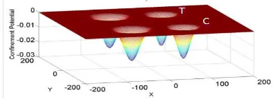
In asymmetric QDs the numerical value of the diameter of larger QD (C1,C2) has been taken as 6nm and for smaller dot
(T1, T2) it has been 4nm. Energy difference of 570 meV has been considered at conduction band. Dots are made up of
InAs and placed on GaAs substrate. The confinement potential of QDs has been considered to be Gaussian in shape and shown in figure 1. The distance from the centres of coupled asymmetric QDs has been p and equal to 6nm and distance from the centres of qubit has been q and equal to 10nm. For simulation to be easy unit considered is AU.
Fig 1: Confinement potential of two asymmetric QD pair, control qubit ‘C’ and target qubit ‘T’.
Input
Output
ε
1ε
2ε
1|ε
1⨁
ε
2|
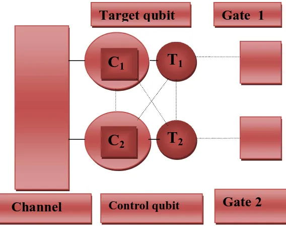
Fig 2: Schematic diagram of CNOT gate using coupled asymmetric QDs solid lines show path of electron tunnelling. Dotted lines show electric fields generated between dots or channel.
By solving the Hamiltonian wavefunction for control qubit has been obtained
− ћ
2m ∂ ∂x +
∂
∂y ѱ+ V(x, y)ѱ= Eѱ
V(x, y) for control qubit has been obtained from the following equation
V(x, y) = exp + exp + x*ξ1
Where ξ1 is the electric field applied through the gate 1 and , gives width of the dot. The wave functions getting
from the above equation gives the probability density of charge resides in control bit. During solving the Hamiltonian of target qubit, coulomb interaction of target qubit has been considered. The potential function for target qubit has been given below;
V(x,y) = exp + exp +
(( ) ( ) )
ѱ+ x*ξ2
Where = ; the relative permittivity of semiconductor QDs, ξ2 is is the electric field applied through the gate 2, x1 and y1 indicates position of wave function of control qubit and x, y indicates position of wave function of target
qubit.
To solve the Hamiltonian imaginary time propagation technique has been used which is given by R. Kosloff and H. Tal-Ezer [11]. This method consists of three steps. First step is setting up a grid and constructing on it an initial wave function. Second step is the calculation of the Hamiltonian and third step is to propagate the wave function in imaginary time.
Target qubit
Gate 1
Gate 2
Control qubit
Channel
C
1
T
2C
2III. RESULTS AND DISCUSSION
Coupled asymmetric QDs have been shown in fig 2 and potential profile for these QDs has been shown in fig 1 for modelling and verification of CNOT gate. When no potential has been applied to gate 1 or gate 2; effects have been observed. The observation has been done for two types. When control bit is in state |0> is first type. For this type wave function obtained has been concentrated in larger dot of control qubit. This concentration of wave function indicates presence of electrons in bigger dot which verify the control bit is in ground state i.e. |0> state and shown in fig 3.
Fig 3: wave function of qubit, at ground state representing state|0>.
Due to coulombic repulsion between control qubit and target qubit potential profile of target qubit has been modified and given in fig 4.
Fig 4: Confinement potential of target qubit constituting the repulsive effect ofthe probability density of electron in control qubit.
For target qubit it has been also noticed that ground state is in larger dot. It means that wave function of electron is concentrated in bigger dot. This concentration of electron gives state |0> of target qubit and shown in fig 5.
Further observation has been made for excited states of target qubit. It has been noticed that the wave function of electron for excited states resides in smaller dot. Occupying of wave function in smaller dot represents |1> state. So this modelling describes target qubit is not affected when the control qubit has state |0> and shown in fig 6.
Fig 6: First Excited state of Target dots, wave function is concentrated at smaller dot corresponding to state |1>.
The second type has been based on control qubit in state |1>. It has been observed that when control bit is in state |1> CNOT gate perform well. In state |1> of control bit the output of CNOT gate flips i.e. if target qubit is in state |0> the output of CNOT gate is state |1> and if target qubit is in state |1> the output of CNOT gate is state |0>. Hence for control bit of state |1> complete logical operation is performed by CNOT gate. In the absence of electric field at any gate the first excited state for control qubit has been concentrated in smaller dot. The wave function is shown in fig 7.
Fig7: wave function of control qubit, at first excited state representing state |1>.
After the addition of coulombic repulsion of target qubit the potential profile to control qubit resulting potential profile is shown in fig 8
.
It has been observed that due to the repulsive force between target qubit and control qubit the wave function of control qubit exchanges target qubit’s ground state (|0>) to state |1> (excited state) and first excited state to state |0> (ground state) are shown below in fig 9 and fig 10.
Fig 9: Ground state wave function of target dots, concentrated at smaller dot corresponding to State |1>.
Fig 10:First Excited state of Target dots, wave function is concentrated at bigger dot corresponding to state |0>.
From the truth table of CNOT gate for one control qubit and one target qubit it has been noticed that this truth table is similar to the truth table of classical XOR gate. For XOR gate the output will be 1 when both inputs are different. Thus CNOT can be used as universal gate. For implementation of universal gate three inputs have been taken. Out of three inputs one input acts as target input and remaining inputs are control input. A special name has been given to this gate, known as Controlled-Controlled NOT (CCN) Gate or Toffoli Gate. CCN gate can perform CNOT operation on target qubit only when both controlled input are in states |1>. Pictorial representation and truth table are given in fig 11 and table 2.
T
T
(
C
1
C
2)
C
2C
2
C
1C
1
Table 2: Truth table of CCN gate when |T> has been used as MSB.
In this truth table when |T> = |0> is fixed then the output |T> will acts as AND gate and when |T> = |1> is fixed then output |T> will acts as NAND gate. Again the output |T> also shows the truth table of XOR gate. Thus from table 2 it has been concluded that a single gate can be acts as AND gate, NAND gate as well as XOR gate.
Pictorial representation and truth table when |C1> acts as MSB are given in fig 12 and table 3.
1
C
C
1
T
C
2
C
2C
2
T
T
Fig12: Scheme of the CCN gate C1 & C2 being control and T being target qubit and C1 acts as MSB.
Table 3: Truth table of CCN gate when |C1> has been used as MSB.
From table 3 it has been observed that when both controlled input |C1> = |0> the |T> output of CNOT gate will be acts
as a Buffer. Again when |C1> is in state |1> then it will be acts as XOR gate. In both table it has been observed that |T>
INPUT
OUTPUT
|T> |C
2> |C
1> |T> |C
2> |C
1>
|0> |0>
|0>
|0> |0>
|0>
|0> |0>
|1>
|0> |0>
|1>
|0> |1>
|0>
|0> |1>
|0>
|0> |1>
|1>
|1> |1>
|1>
|1> |0>
|0>
|1> |0>
|0>
|1> |0>
|1>
|1> |0>
|1>
|1> |1>
|0>
|1> |1>
|0>
|1> |1>
|1>
|0> |1>
|1>
INPUT
OUTPUT
output will change its state when both controlled input are in state |1> and acts as NOT gate. Thus from table 2 and table 3 it has been concluded that quantum controlled NOT gate can acts as universal gate.
IV. CONCLUSION
The concept of CNOT gate has been demonstrated. For simulation of two qubits CNOT orbital states of electrons have been employed. Simulation results verify the action of control qubit for manoeuvring the logic levels of target qubit. Also it is verified with the simulations that target qubit changes it’s state only when control qubit is high. Further two qubits CNOT gate has been extended to three qubit CCN gate. In the extended truth table it has been observed that when target qubit is controlled and it is fixed to performs logical AND operation, logical NAND operations and logical XOR operation. In the second case, first control qubit is fixed to lower state, to get target to act as buffer. Thus it can be concluded that by keeping anyone of the qubit fixed various type of logic gate can be formed. Thus CCN can be used to work as Universal gate.
REFERENCES
[1] A. Barenco, D. Deutsch and A. Ekert, "Conditional Quantum Dynamics and Logic Gates," Physical Review, vol. 74, no. 20, pp. 4083-4086, 1995. [2] J. Levy, "Quantum-information processing with ferroelectrically coupled quantum dots," Physical Review A, vol. 64, no. 5, pp. 52306-52312, 2001.
[3] M. Feng, "A scheme of quantum computing with semiconductor quantum dots in optical cavity," Physics Letters, vol. 306, no. 5-6, pp. 353-357, 2003.
[4] B. E. Kane, "A silicon-based nuclear spin quantum computer," Nature, vol. 393, pp. 133-137, 1998.
[5] T. Tanamoto, "Quantum gates by coupled asymmetric quantum dots and controlled-NOT-gate operation," Physical Review,, vol. 61, no. 2, pp. 22305-223011, jan 2000.
[6] S. Moskal, S. Bednarek and a. J. Adamowski, "Controlled exchange interaction for quantum logic operations with," Physical Review, vol. 76, p. 32302, 2007.
[7] C. H. Bennett and D. P. DiVincenzo, "Quantum information and computation," Nature, vol. 404, pp. 247-255, 2000.
[8] A. Einstein, B. Podolsky and N. Rosen, "Can Quantum-Mechanical Description of Physical Reality Be Considered," Physical Review, vol. 47, pp. 777-780, 19335.
[9] A. A. Balandin and K. L.Wang, "Implementation of Quantum Controlled-NOT Gate using Asymmetric," in First NASA conference; QCQC, California, USA,, 1998.
[10] C. C.H.Crouch, C. Livermore, R. M. Westervelt, K. L. Campman and A. C. Gossard, "Evolution of the Coulomb gap in tunnel-coupled quantum dots,," Applied Physics Letters, vol. 71, no. 6, p. 817, 1997.
[11] F. R. Waugh, "Single-Electron Charging in Double and Triple Quantum Dots with Tunable Coupling,," Physical Review,, vol. 75, no. 4, pp. 705-708, 1995.