Power Flow Control of Photovoltaic Power
Generation System Using Five-Level Inverter
Kondreddy Harshitha1, T. Suneel Kumar2
PG Student [EPS], Dept. of EEE, Sree Vidyanikethan Engineering College, Tirupati, Andhra Pradesh, India1 Assistant Professor, Dept. of EEE, Sree Vidyanikethan Engineering College, Tirupati, Andhra Pradesh, India2
ABSTRACT: Generally, the output from the PV array is a DC power so, an inverter is necessary to inject that power into the grid. In this paper, a five-level inverter with dual-buck topology is used. The dual-buck converter converts the DC power into three DC voltage levels i.e., 0,Vdc/2,Vdc. Due to this conversion, the number of switches used in five-level inverter is reduced. Further, the three five-level DC voltage is converted into five-five-level AC voltage with the help of full-bridge inverter. As a result, the switching losses and harmonic distortions are reduced. A Boost converter is used to boost the output voltage of solar array. The switching control of IGBT of boost converter is obtained by perturb and observe method. This entire module is developed in SIMULINK.
KEYWORDS: Inverter, Switching losses, harmonic distortions, Perturb and observe method.
I.INTRODUCTION
The renewable energy generation has been assuming increasing significance now-a-days because of the growing concern towards country's energy security. Day-by-day the energy scenario is changing. so, an intensified research on renewable energy generation has lead to the emergence of various methods involving energy resources like solar, wind etc., basically, all kinds of energy on earth originate in solar energy. so it is possible to use solar energy for various applications. the solar PV contributes 4.59% of the renewable energy installed capacity in India[1]
However, the renewable energy sources needs the power electronic interface to the utility grid because of various power conversions being involved between the sources and the grid. An inverter plays a major role for this power conversion. The multilevel inverters presents great advantage when compared to two-level inverters. These advantages are fundamentally focused for the improvement of output signal quality. As the number of levels increases, the THD of the inverter output remains less when compared to two-level inverters.
while considering all these advantages, the multilevel inverters also have some limitations. The converter control is complex when compared to conventional inverter topologies. Balancing of DC capacitor voltages, high switching losses etc., remains a serious issue[2].
The predominantly used multilevel inverter topologies are the neutral point clamped (NPC)type, flying capacitor (FC)type, cascaded H-bridge (CHB) type. these different types of inverters has been successfully commercialized for very high power and power quality demanding applications at various power ratings.
This paper reveals the working and simulation of a new five-level inverter topology which proves to overcome some of the limitations of conventional multilevel topologies.
II
.
PROPOSED TOPOLOGYdone and converts into a DC output voltage with three levels. Finally, the output of the dual-buck converter is connected to the full-bridge inverter to convert the three-level DC voltage into five-level AC voltage[3]. Fig. 1 shows the circuit configuration of the five-level inverter applied to a photovoltaic power generation system.
Fig. 1 circuit configuration of photo voltaic power generation system of five level inverter with dual-buck converter topology
III. OPERATING PRINCIPLE
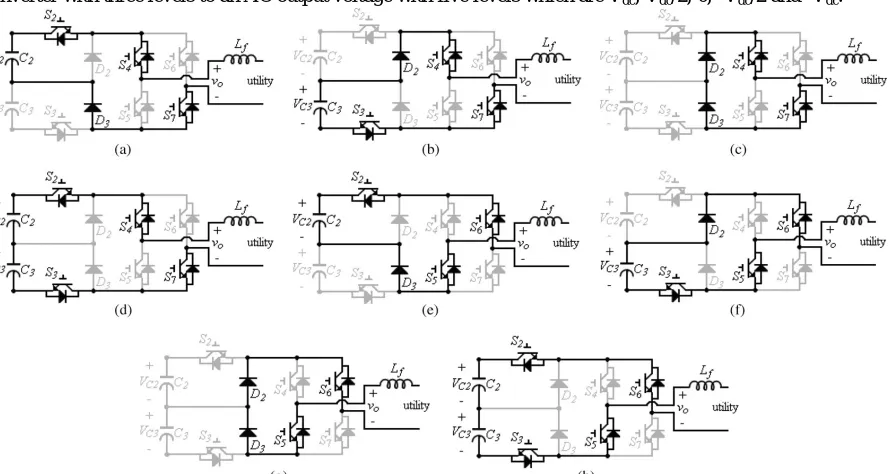
The operation of the five-level inverter is categorized into eight modes. The modes 1-4 are for positive half cycle and the other modes 5-8 are for the negative half cycle. Fig. 2 shows the operating modes of five-level inverter. The power electronic switches i.e., IGBT's of the full-bridge inverter are switched in low frequency and is synchronous with the utility voltage to convert the DC power into AC power. As seen in Fig. 2(a)-(d), the power electronic switches S4 and S7 are in ON state, and the corresponding S5 and S6 are in OFF state. Similarly, the power electronic switches S4 and S7 are in OFF state and the necessary S5 and S6 are in ON state for negative half-cycle. The DC capacitor voltages VC2 and VC3 are balanced by controlling the five-level inverter as explained above. The DC capacitor voltages VC2 and VC3 can be represented as follows:
dc c
c
V
V
V
2
1
32
The modes of operation of the five-level inverter are stated follows.
Mode 1: Fig. 2(a) shows the circuit operation of mode 1. The power electronic switch of the dual-buck converter S2 is turned ON and S3 is turned OFF. The DC capacitor C2 is discharged through S2, S4, the filter inductor, the utility, S7 and D3 to form a loop. The output voltage values of dual-buck converter and five-level inverter are Vdc/2.
Mode 2: Fig. 2(b) shows the circuit operation of mode 2. The power electronic switch of the dual-buck converter S2 is turned OFF and S3 is turned ON. The DC capacitor C3 is discharged through D2, S4, the filter inductor, the utility, S7 and S3 to form a loop. The output voltage values of dual-buck converter and five-level inverter are Vdc/2.
Mode 3: Fig. 2(c) shows the circuit operation of mode 3. The power electronic switches S2 and S3 of the dual-buck converter are turned OFF. The stored current in the filter inductor flows through the utility, S7, D3, D2 and S4. The output voltage values of dual-buck converter and five-level inverter are zero.
Mode 4: Fig. 2(d) shows the circuit operation of mode 4. The power electronic switches S2 and S3 of the dual-buck converter are turned ON. The DC capacitors C2 and C3 are discharged together through S2, S4, the filter inductor, the utility, S7 and S3 to form a loop. The output voltage values of dual-buck converter and five-level inverter are Vdc.
The same process repeats for negative half cycle with modes 5-8. Here, the power electronic switches S4 and S7 are in OFF state and corresponding S5 and S6 switches are in ON state.
By considering these operating modes 1-8, the full-bridge inverter converts the DC output voltage of the dual-buck converter with three levels to an AC output voltage with five levels which are Vdc, Vdc/2, 0, -Vdc/2 and -Vdc.
Fig. 2 Operation modes of the five-level inverter. (a) Mode 1 (b) Mode 2 (c) Mode 3 (d) Mode 4. (e) Mode 5. (f) Mode 6. (g) Mode 7. (h) Mode 8.
IV.VOLTAHE BALANCE OF FIVE-LEVEL INVERTER
The voltage balancing between two DC capacitors is very important in controlling the multi-level inverter. Here, voltage balance of DC capacitor voltages VC2 and VC3 can be controlled by the power electronic switches S2 and S3. When the absolute value of the utility voltage is smaller than Vdc/2, one power electronic switch either S2 or S3 is switched in high frequency and the other is still in OFF state. The voltage value of the DC capacitor VC2 or VC3 will decide the ON/OFF states of power electronic switches S2 and S3.
If VC2 is higher than VC3 the power electronic switch S2 is switched in high frequency. In this condition, the voltage source VCx in Fig. 3(a) is equal to VC2, and C2 is discharged. Thus VC2 decreases and VC3 does not change. On the contrary, if VC3 is higher than VC2 the power electronic switched frequency. In this condition, the voltage source in Fig. 3(a) is equal to VC3. Thus the DC capacitor voltage VC3 decreases and VC2 does not change. The voltage balance of C2 and C3 can be achieved in this way.
Fig. 3 Equivalent circuit. (a) |vs |< Vdc /2. (b) |vs |> Vdc /2
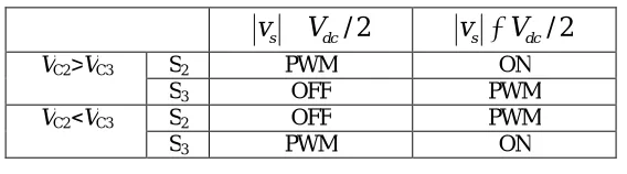
electronic switch (S2 or S3) is switched in high frequency can be found out. If VC2 is higher than VC3, the power electronic switch S3 is switched in high frequency and the voltage source VCx in Fig. 3(b) is equal to VC2. when S3 is turned ON, both C2 and C3 are discharged. However, when S3 is turned OFF only C2 supplies the power. In the same way, when VC3 is higher than VC2 the power electronic switch S2 is switched in high frequency and the voltage source VCx in Fig. 3(b) is equal to VC3. When S2 is turned ON, both C2 and C3 are discharged. However, when S2 is turned OFF only C3 supplies the power. In this way, the voltage balance of C2 and C3 can be achieved. The logic for operation of power electronic switches S2 and S3 is represented in Table I.
Table I: ON/OFF states of S2 and S3
2
/
dc
s
V
v
v
s
V
dc/
2
VC2>VC3 S2 PWM ON
S3 OFF PWM
VC2<VC3 S2 OFF PWM
S3 PWM ON
V. CONTROL BLOCK DIAGRAM
The photovoltaic power generation system consists of a DC–DC power converter and the level inverter. The five-level inverter configured with dual-buck converter and full-bridge inverter performs the functions of converting the DC power into high-quality AC power and injecting it into the utility, balancing two dc capacitor voltages VC2 and VC3, and
detecting the islanding operation. The DC-DC Boost converter boosts the output voltage of the solar cell array and performs the MPPT to extract the maximum output power of the solar cell array. A control logic has been developed for the generation of PWM pulses in both five-level inverter and DC-DC Boost converter. The controllers of both the DC-DC Boost Converter and five-level inverter are explained as follows:
A. Five-Level Inverter
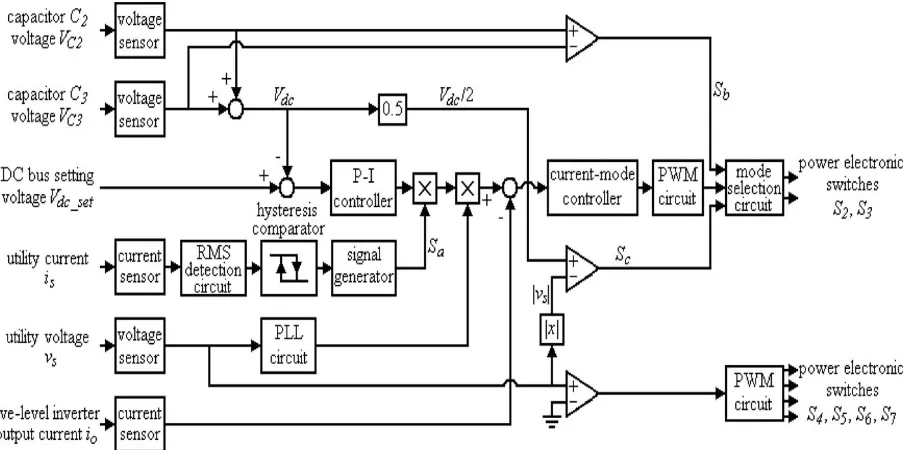
In the operation of the five-level inverter, the dc bus voltage must be regulated to be larger than the peak voltage of the utility and the dc capacitor voltages of C2 and C3 must be controlled to be equal. Besides, the five-level inverter must generate a sinusoidal current in phase with the utility voltage to be injected into the utility. As seen in Fig. 4, the voltages of dc capacitors C2 and C3 are detected and then added to obtain a dc bus voltage Vdc. The added result is subtracted from a dc bus setting voltage Vdc set. The dc bus setting voltage Vdc set is larger than the peak voltage of the
utility. The subtracted result is sent to a PI controller An islanding detection is also incorporated into the control of the five-level inverter.
As seen in Fig. 4, the utility current is detected and sent to an RMS detection circuit. The output of the RMS detection circuit is sent to a hysteresis comparator that contains a low threshold value and a high threshold value. If the RMS value of the utility current is smaller than the low threshold value, the output of the hysteresis comparator is high, meaning the condition of islanding operation or power balance occurs. On the contrary, the output of the hysteresis comparator is low when the RMS value of the utility current is larger than the high threshold value, meaning the utility is normal. The output of the hysteresis comparator is sent to a signal generator. The output signal of the signal generator is an islanding control signal Sa. The islanding control signal is a dc signal with unity amplitude if the output
capacitor voltage VC2 is higher than dc capacitor voltage VC3, Sbis a high value. On the contrary, Sbis a low value when
dc capacitor voltage VC2 is smaller than dc capacitor voltage VC3 . DC voltage Vdc is also sent to an amplifier with a gain
of 0.5 to obtain voltage signal Vdc/2. The detected utility voltage is sent to an absolute circuit to obtain voltage signal |vs
|. Voltage signals Vdc/2 and |vs | are compared to obtain signal Sc . When Vdc/2 > |vs |, Sc is a high value. On the
contrary, Scis a low value when Vdc/2 < |vs|. The output signal of the PWM circuit and signals Sband Scare sent to the
mode selection circuit. The output of the mode selection circuit will generate the control signals of power electronic switches S2 and S3 according to Table I. The detected utility voltage is also sent to a comparator to obtain complementary square signals that are synchronous with the detected utility voltage. The complementary square signals are the control signals of the power electronic switches of the full-bridge inverter. As mentioned earlier, only two power electronic switches S2 or S3 in the five-level inverter should be switched in high frequency, and only one of them is switched in high frequency at any time, and the voltage level of every switching is Vdc/2. Therefore, the five-level inverter can reduce the switching loss effectively.
Fig. 4 Control block diagram of five-level inverter.
B. DC-DC Boost converter
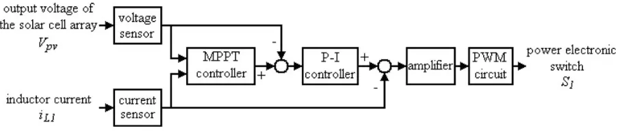
Theinput of the DC-DC Boost converter is the output of the solar cell array. A ripple voltage with a frequency double that of the utility will appear in the dc bus voltage Vdc, while the five-level inverter injects real power into the utility. The function of MPPT will be degraded, while the output voltage of solar cell array contains a ripple voltage. Therefore, the ripple voltage super imposed on the DC bus voltage Vdc must be blocked by the DC–DC Boost converter for improving the function of MPPT. Accordingly, the dual control loops, an outer voltage control loop, and an inner current control loop are applied to control the DC–DC Boost converter as shown in Fig. 5. Since the output voltage of the DC–DC Boost converter is the DC bus voltage that is controlled to be a constant voltage by the five-level inverter, the outer voltage control loop is used to regulate the output voltage of the solar cell array. The inner current control loop is applied to control the inductor current to approach a constant current to block the ripple voltage of dc bus voltage Vdc. The perturbation and observation method is adopted to obtain the function of MPPT, and it is incorporated into the controller of the DC– DC Boost converter. The output of the MPPT controller is the desired output voltage of the solar cell array, and it is the reference voltage of the outer voltage control loop. The output voltage of the solar cell array is perturbed first, and then the output power variation of the solar cell array is observed to determine the next perturbation for the output voltage of the solar cell array.
to a MPPT controller to determine the desired output voltage of the solar cell array. The detected output voltage and desired output voltage of the solar cell array are sent to a sub tractor, and the subtracted result is sent to a PI controller. The output of the PI controller is the reference signal of the inner current control loop. The reference signal and the detected inductor current are sent to a sub tractor, and the subtracted result is sent to an amplifier to complete the inner current control loop. The output of the amplifier is sent to the PWM circuit. The output signal of the PWM circuit is the driving signal for the power electronic switch of the DC–DC Boost converter.
Fig. 5 Control block of DC-DC Boost converter
For protecting the renewable power generation system from the voltage rise, the MPPT function will be disabled and the power electronic switch S1 will be turned OFF when the inverter stage is interrupted after detecting the islanding operation. Therefore, the output voltage of solar cell array is limited to the open-circuit voltage of solar cell array, and the dc bus voltage Vdc is also limited.
VI.CONCLUSION
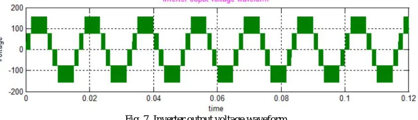
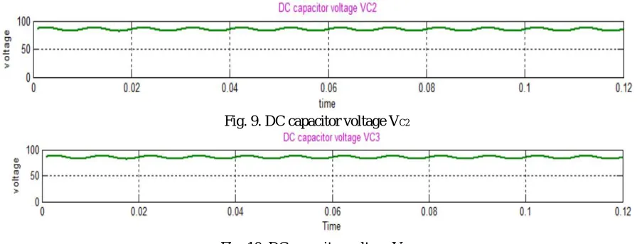
The proposed five-level inverter is simulated using MATLAB/SIMULINK software to verify that the proposed inverter can be practically implemented in a PV system. The photovoltaic power generation system is developed for injecting the real power into the grid by using a five-level inverter to reduce losses and also to increase performance. The grid voltage was chosen to be 110V and the DC voltage was chosen as 170V since it must be greater than peak of grid voltage. Waveforms of grid voltage, inverter output current, inverter output voltage and capacitor voltages were obtained. Fig. 6 shows the grid voltage waveform, Fig. 7 shows inverter output voltage, Fig. 16 shows the current ripple of DC-DC Boost converter which is obtained with 1.6% current ripple by using a filter inductor of 5mH. The THD of inverter current was found to be 0.04%. THD% of inverter output was found to be 26.89%. The voltage of dc link capacitors shown in Fig. 9 and Fig. 10 were found to be balanced and each of the two capacitors stores 82.5V with a voltage ripple less than 5%.
Table II: Parameters used in Simulation
DC bus capacitor (C2 and C3) 2,200 µF Filter inductor (Lf) 2mH DC bus setting voltage 170V Switching frequency (PWM) 20kHz
Utility voltage 110V Utility frequency 60Hz Load resistor 100Ω
Fig. 6.Grid voltage waveform
Fig. 6 shows the experimental results of the utility voltage at the grid side i.e., 110V. This waveform is generated to match the obtained five-level output voltage with the peak voltage of the utility by converting the real power that is obtained for PV system so as to distribute the maximum output power in the form of AC to domestic loads.
Fig. 7. Inverter output voltage waveform
Fig. 7 shows the experimental results for the five-level inverter used in the developed photovoltaic power generation system under steady state at five voltage levels Vdc, Vdc/2, 0, -Vdc, -Vdc/2 by the full-bridge inverter. The voltage variation of each level is Vdc/2. The output voltage waveform indicates the maximum voltage of 170V. This verifies that the five-level output AC voltage according to the utility voltage as explained above in the operating principle.
Fig. 8.dual-buck converter voltage waveform
Fig. 9. DC capacitor voltage VC2
Fig. 10. DC capacitor voltage VC3
Fig. 9 and Fig. 10 shows the DC capacitor voltages VC2 and VC3 remain in balance, and their voltage is about 85V, respectively.
Fig. 11. Driver signal of S5
Fig. 12. Driver signal of S4(complementary square signal)
Fig. 11 and Fig. 12 shows the pulse generation of switches S5 and S4. The switching frequency of the switches is 60Hz.
Fig. 13. Input current of full bridge inverter
Fig. 13 shows the absolute value of the output current of the full-bridge inverter. The power electronic switches of the full-bridge inverter are switched in low frequency, and the full bridge inverter can convert the DC power into AC power.
Fig. 15. Voltage ripple of DC capacitor C3
Fig. 14 and Fig. 15 shows the peak-to-peak value of the voltage ripple at DC capacitors C2 and C3 is about 5V.
Fig. 16. Current ripple of DC-DC converter
Fig. 16 shows the ripple of inductor current is very small due to the use of the current mode control.
Fig. 17. Voltage ripple of solar cell
Fig. 17 shows the peak-to-peak value of the voltage ripple at the solar cell array is very small.
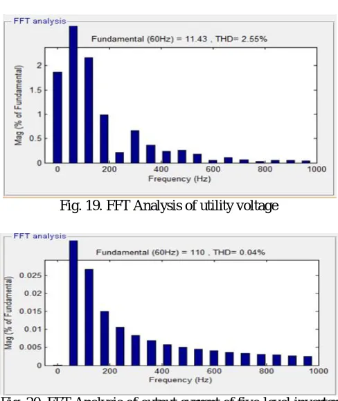
Fig. 19. FFT Analysis of utility voltage
Fig. 20. FFT Analysis of output current of five-level inverter
From Fig. 19 and Fig. 20, it can be seen that the total harmonic distortion(THD%) of the utility voltage and the output current of the five-level inverter are 2.55% and 0.04% respectively.
Table III Comparison of different multi-level inverters
Diode clamped
Flying capacitor
Cascaded H-bridge
Developed inverter
Power electronic switches 8 8 8 6
capacitors 2 4 2 2
Voltage balance of capacitors Hard Hard Hard Easy
High frequency switches 8 8 8 2
VI. CONCLUSIONS
REFERENCES
[1] M. Calais and V. G. Agelidis, “Multilevel converters for single-phase grid connected photovoltaic systems—An overview,” in Proc. IEEE Int. Symp. Ind. Electron., 1998, vol. 1, pp. 224–229.
[2] J. M. Carrasco, L. G. Franquelo, J. T. Bialasiewicz, E. Galvan, R. C. Portillo Guisado, M. A. M. Prats, J. I. Leon, and N. Moreno-Alfonso, “Power-electronic systems for the grid integration of renewable energy sources: A survey,” IEEE Trans. Ind. Electron., vol. 53, no. 4, pp. 1002– 1016, Aug. 2006.
[3] Jia-Min Shen, Hurng-LiahngJou, Jinn-Chang Wu and Kuen-Der Wu, “Five-Level Inverter for Renewable Power Generation System,” IEEE Trans. Energy Conversion, vol. 28. no. 2, pp. 257-266, June 2013.
[4] Muhammad H. Rashid, Power electronics circuits, devices & applications, Pearson Education, Inc., 3rd edition, 2004.
[5] Debashis Das,Shishir Kumar Pradhan, “Modeling and simulation of PV array with boost converter”, B-Tech thesis, NIT Rourkela, 2011. [6] J. M. Carrasco, L. G. Franquelo, J. T. Bialasiewicz, E. Galvan, R. C. Portillo Guisado, M. A. M. Prats, J. I. Leon, and N. Moreno-Alfonso,
“Power-electronic systems for the grid integration of renewable energy sources: A survey,” IEEE Trans. Ind. Electron., vol. 53, no. 4, pp. 1002– 1016, Aug. 2006.
[7] S. De, D. Banerjee, K. Siva Kumar, K. Gopakumar, R. Ramchand, and C. Patel, “Multilevel inverters for low-power application,” IET Power Electron., vol. 4, no. 4, pp. 384–392, Apr. 2011.
[8] S. J. Park, F. S. Kang, M. H. Lee, and C. U. Kim, “A new single-phase five level PWM inverter employing a deadbeat control scheme,” IEEE Trans. Power Electron., vol. 18, no. 18, pp. 831–843, May 2003.
[9] G. P. Adam, S. J. Finney, B. W. Williams, and M. T. Mohammed, “Two level operation of a diode-clamped multilevel inverter,” in Proc. IEEE Int.Symp. Ind. Electron., Jul. 2010, pp. 1137–1142.