ISSN (Print) : 2320 – 3765 ISSN (Online): 2278 – 8875
I
nternational
J
ournal of
A
dvanced
R
esearch in
E
lectrical,
E
lectronics and
I
nstrumentation
E
ngineering
(A High Impact Factor, Monthly, Peer Reviewed Journal)
Website: www.ijareeie.com
Vol. 7, Issue 11, November 2018
Design of a Clock Distribution Network using Low
Power Prescaler and Fused P & S Counters
Alapati Raja Mahesh Krishna Teja1, P.Aditya Ratna Chowdary2
PG Student [VLSI], Dept. of ECE, Sai Tirumala NVR Engineering College, Jonnalagadda, India1
Assistant Professor, Dept. of ECE, Sai Tirumala NVR Engineering College, Jonnalagadda, India2
ABSTRACT: In this paper we have shown the design of clock distribution network using 2/3. In wireless
communication applications like WLAN, ZIGBEE, Bluetooth etc. frequency synthesizer is the major component. The speed of the frequency synthesizer depends up on the prescaler and Voltage controlled oscillator. 2/3 prescaler has to implement using TSPC (true single phase clock) or ETSPC (Extended true single phase clock) and flip flops. In this paper we propose prescaler with embedding two NOR gates in the two stages of prescaler design instead of using one AND gate and one OR gate. The two designs are compared in terms of power. Using the proposed prescaler we have designed clock distribution network which can divide by 2,3,4,5,32,33,47,48 etc. prescaler implemented with 180nm technology can operate up to 5Ghz frequency. This system also concentrates to combine programmable and swallow counters. Clock distribution network system code written in verilog, modeled using Xilinx and Modelsim.
KEYWORDS: TSPC, ETSPC, Frequency Synthesizer, Prescaler, clock distribution.
I. INTRODUCTION
In frequency synthesizers high speed dual modulus prescaler is an important lock which uses pulse swallow frequency dividers. The prescaler operates at the very best frequencies and consumes additional power than alternative circuit blocks of the frequency synthesizer [1].The E-TSPC concept was introduced in [2] and it is further developed in [3]. The E-TSPC based mostly prescaler is projected in several technique to avoid surplus power consumption in [14] as technique 2.In this technique 2 and gates are used rather than one or gate and one AND gate to achieve a 2/3 prescaler with least power consumption. A TSPC design was proposed by using 130nm CMOS technology in [4]. In [5] TSPC dual modulous have been proposed by using two NOR gates. By using current leakage restricting transistors at the nodes modulous design have been discussed based on stage merged scheme in [6]. The different TSPC, multi modulous techniques have been discussed in [7]-[13].
In synchronous circuits clock signal is very important to synchronize the input data signals which arrive from the different sources of the digital Integrated circuit. There are many factors effects the synchronization of signals like noise, delay and with the same clock reaching the memory register known as clock jitter causing in phase noise[14]. Prescaler concept have introduced in the clock distribution network [15]. Generally prescaler generates an output signal by a fractional rate for a given input signal [15].
Prescaler is a synchronous, which is built by D-flip flops and by using the different logic gates. In frequency synthesizer prescaler is the crucial component which performs the dividing operation.In VLSI technology the research mainly concentrates on the three optimizations. Those are power, area and delay. Out of total components of frequency synthesizer prescaler circuit consumes more power. In prescaler circuit clock signal consumes nearly more than half of the total power consumption because clock signal has more switching. Prescaler mainly has two division ratios ‘N’ and ‘N+1’ [13]. A frequency synthesizer uses phased locked loop (PLL) and PLL uses prescaler as a critical component. Prescaler has designed by many researchers.The E-TSPC 2/3 prescaler reported in [16] consumes giant shortcircuit power and contains a higher frequency of operation than that of 2/3 prescaler. In [16], a gate-integrated dual-modulus prescaler supported the dynamic circuit has been planned to attain the high operative frequency and low power consumption. This style uses 2 DFFs, whereas the divide-by-4/5 unit in [25] uses 3 DFFs.
ISSN (Print) : 2320 – 3765 ISSN (Online): 2278 – 8875
I
nternational
J
ournal of
A
dvanced
R
esearch in
E
lectrical,
E
lectronics and
I
nstrumentation
E
ngineering
(A High Impact Factor, Monthly, Peer Reviewed Journal)
Website: www.ijareeie.com
Vol. 7, Issue 11, November 2018
PMOS transistor is connected between power supply and DFF1. The DFF1 doesn’t participate in divide-by-2 operation solely DFF2 participates. The MC is control logic signal that is given as input to additional PMOS transistor. This DFF1 switches off utterly during divide-by-2 mode [1][14].
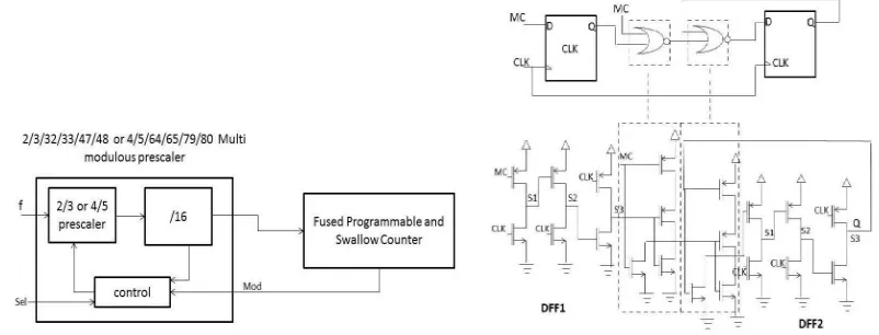
The wideband single-phase clock 2/3 prescaler was projected in [15]. In this design it neither consists of 2 D-flip-flops and 2 NOR gates embedded within the flip-flops. The primary NOR Gate is not embedded within the last stage of DFF1, and the second NOR gate is embedded within the 1st stage of DFF2. This design focused primarily on low power consumption. Figure 1 shows the complete clock distribution network with prescalers.
This paper is organized as section II discuss about the proposed design, Section III illustrates Multi modulous prescaler, Section IV describes about fused programmable and swallow counters, Section V shows simulations of the design and section VI concludes the paper.
Fig .1 Clock distribution network
Fig. 2 Proposed single-phase clock 2/3 Prescaler
II. PROPOSED DESIGN
In digital circuits delay and power consumptions are the key parameters. Maximum operating frequency of a digital circuit can be calculated as [15] [1]
fmax=1/(tpHL+tpLH)
tpHL, tpLHare the gate delays. The combination of switching and short circuit powers will determine the total power consumption of the digital circuit. Switching power depends mainly on the operating frequency, load capacitance and power at each output node as [15] [1]
Psw= fclkClVdd2
Vdd is the supply voltage, Cl is the load capacitance and fclk is the clock frequency. When there are direct paths to the ground from supply causes to short circuit power to occur as
Psc=Isc*Vdd Isc is the short circuit current.
ISSN (Print) : 2320 – 3765 ISSN (Online): 2278 – 8875
I
nternational
J
ournal of
A
dvanced
R
esearch in
E
lectrical,
E
lectronics and
I
nstrumentation
E
ngineering
(A High Impact Factor, Monthly, Peer Reviewed Journal)
Website: www.ijareeie.com
Vol. 7, Issue 11, November 2018
The proposed divide-by-2/3 prescaler unit in is shown in Fig. 2. The proposed prescaler uses a simple architecture with E-TSPC consists of two Dflip flops and two NOR gates. When logic signal MC switches from “one” to “zero,” the logic worth at the input of DFF1 is transferred to the input of DFF2 collectively of the input of the NOR gate embedded in DFF1 is “0” and therefore the band prescaler operates at the divide-by-3 mode. Throughout the divide-by-2 operation, solely DFF2 actively participates within the operation and contributes to the full power consumption since all the change activities are blocked in DFF1. Thus, the band 2/3 prescaler has advantage of saving quite five hundredth of power throughout the divide-by-2 operation.
It once the modulus management signal Mc is logically low, it performs the divide-by-3 operate. If the output of DFF2 is logically low, the node point S1 of DFF2 is disabled, therefore nodes S2 and S3 of DFF2 can haven't any switch activities,and hence there will be no switch power dissipation.DFF1 operates all the time, whereas DFF2 exclusively operates once the output of DFF2 is logically high. Once MC is logically high, the output of DFF1 is going to be disabled to realize the divide-by-2 function. However, the nodes S1 and S2 of DFF1 still have switch activities since the output of DFF2 still feeds back to DFF1. Thus each DFFs switch at half the input frequency even though DFF1 doesn't participate within the divide-by-2 function. As a result, the divide-by-2 unit dissipates a lot of power even as long as one toggled DFF is required. Such a topology introduces unneeded power consumption, that may be a vital a part of the whole power consumption. Moreover, throughout 1 / 4 of the period, the short-circuit power still exists in DFF1. The troublesome of low-power style for the divide-by-2/3 unit is to attenuate the power consumption. throughout the divide- by-2 operation, it's not necessary for each DFFs to control at full speed since just one toggled DFF is required to perform the divide-by-2 operate. If just one DFF is active throughout the divide-by-2 operation, on paper a five hundredth reduction of power consumption is achieved.
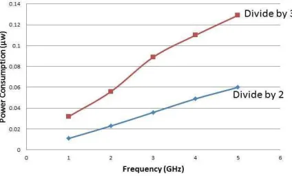
As wave propagation in buildings can vary widely according to configuration, the maximum distance between two network nodes can be specified in free range (i.e. without any obstacles) and usually lies between 10 and 100m. For most sensing applications, nodes spend far more time receiving than emitting Therefore, even though the power level required in transmits mode is an order of magnitude higher, the receiver power consumption is most critical.In our case, the target was not higher than 1μW’ (l mA, 1.5V supply) in order to obtain a sufficient battery lifetime.Fig. 3 shows the power consumption characteristics with frequency. Fig. 3 shows the power consumption characteristics with frequency. This high power consumption is especially because of the primary stages of the frequency divider that usuallydissipates half the full power [17-23].
III. MULTIMODULUS 32/33/47/48 PRESCALER
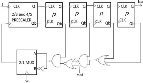
The projected broadband multimodulusprescaler which divides the input frequency by thirty two, 33, 47, and forty eight etc. is shown in Fig. 4. It is kind of like the 32/33 prescaler utilized in, however with an extra multiplexer and a transistor. The projected prescaler performs extra divisions (divide- by-47 and divide-by-48) with none additional flip-flop, therefore saving a substantial quantity of power and additionally reducing the quality of multiband.
ISSN (Print) : 2320 – 3765 ISSN (Online): 2278 – 8875
I
nternational
J
ournal of
A
dvanced
R
esearch in
E
lectrical,
E
lectronics and
I
nstrumentation
E
ngineering
(A High Impact Factor, Monthly, Peer Reviewed Journal)
Website: www.ijareeie.com
Vol. 7, Issue 11, November 2018
The multimodulus prescaler consists of the broadband 2/3 (N1/ (N+1)) prescaler [13], 4 asynchronous TSPC divide-by-2 circuits ((AD) =16) and combinatory logic circuits to attain multiple division ratios. Beside the same old MOD signal for dominant N (N+1) divisions, the extra management signal Scl is used to change the prescaler between 32/33 and 47/48 modes.
Fig. 4 Proposed Multimodulus 32/33/47/48 or 64/65/79/80 Prescaler
Case 1: Sel=’0’
When Sel=0 , The 2/3 prescaler takes the input from the NAND2 directly and when logic signal MOD controls the division quantitative relation the multimodulus prescaler operates as 32/33 prescaler.The 2/3 prescaler operates in divide by 3 mode in the second stage and divide by 2 mode when MC=1.
If MOD =1, For the entire operation the broad band prescaler operates in divide by 2 mode when NAND2 switches to logic 1. The division magnitude relation N performed by the multimodulus prescaler is [2]
N = (AD*N1)+(0*(N1+1)) = 32
Where N=2 and AD=16 is mounted for the whole style. MC always be 1 for MOD=0 and the Third input clock cycles, and MC will be 0 when prescaler operates in divide by 2 mode and multiple input clock cycles. When the broadband prescaler operates in divide by 3 mode MC will be logic 0. The division ratio N+1 performed by the multi modulus prescaler is
N + 1 = ((AD – 1)*N1)+(1*(N1+1)) =33 Case 2: Sel = 1
When Sel = 1, The 2/3 prescaler takes the input from the inverse output of the NAND2 gate and thus the multimodulus prescaler operates as a 47/48 prescaler, wherever the division magnitude relation is controlled by the logic signal MOD. If MC = 1, the 2/3 prescaler operates in divide-by-3 mode and once MC=0, the 2/3 prescaler operates in divide-by-2 mode that is kind of opposite to the operation performed once Sel=0.
If MOD = 1, the division quantitative relation N+1 performed by the multi modulus prescaler is same as except that the broadband prescaler operates within the divide-by-3 mode for the whole operation can be
N + 1 = ((AD *(N1+1))+(0*N1)) = 48
If MOD = 1, The multi modulus prescaler with the division N at MOD=1 will be N = ((AD - 1) * (N1+1)) + (1*N1) = 47
The prescaler acts as 4/5 prescaler by adding an extra multiplexer selection line is one, N = (AD*N1)+(0*(N1+1))=64
Where N1=4 and AD=16.
N + 1 = ((AD – 1)*N1)+(1*(N1+1))=65 When Sel=1:
N + 1 = ((AD *(N1+1))+(0*N1))=80 Where N1=4 and AD=16.
ISSN (Print) : 2320 – 3765 ISSN (Online): 2278 – 8875
I
nternational
J
ournal of
A
dvanced
R
esearch in
E
lectrical,
E
lectronics and
I
nstrumentation
E
ngineering
(A High Impact Factor, Monthly, Peer Reviewed Journal)
Website: www.ijareeie.com
Vol. 7, Issue 11, November 2018
IV. FUSED P&S COUNTERS
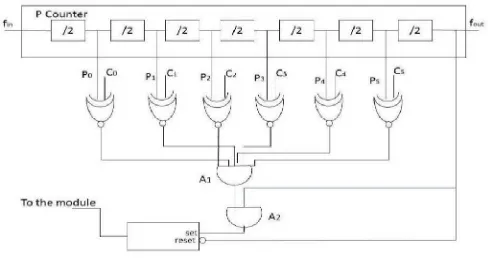
Fig. 5 shows as the diagram of consolidated P&S counter. Because it is evident, this counter consists of a divide-by-128 (P counter) that's created of seven divide-by-2. The XNOR gate (X0-X5), AND gates and a flip flop WHICH is RSFF consists in the digital circuit. This digital section has replaced S counter in typical ones and has the duty to manage modulus bit of dual modulus prescaler. XNOR gates (X0 – X5) the A1gate. Once inputs of XNOR are equal (both of them are zero or 1), output of XNOR gate is logic one. Therefore once the value of P counter (P6P5P4P3P2P1P0) is adequate predefined C variety (C1C5C4C3C2C1C0), output of A1 gate becomes logic. Throughout this moment, as P6 is 1 conjointly, RSFF was set by A2 gate and dual modulus prescaler divide input frequency by N. once P6 changes to zero, RSFF is reset and twin modulus prescaler return to divide-by-(N + 1) state. For added details, assume the P counter is ZERO condition. As P6 is adequate zero, RSFF is reset and twin modulus prescaler divides input frequency by (N + 1). Thus as for the PLL to work in sixth frequency channel which we tend to load the amount of vi on C5-C0. Input signal is applied and P counter will increase till the worth of P counter reaches the predefined C. (For this example: P6P5P4P3P2P1P0=1000110). During this worth of P counter, output of XNOR blocks and P6 are logic one that causes RSFF to be set by A1 and A2 gates. When now, the prescaler divide input frequency by N until the P counter reaches to its maximum worth (1111111) and next worth is 0000000. RSFF is reset by P6, prescaler returns to divide-by- (N + 1) scenario and also the cycle repeats once more. During this cycle the events occurred almost like typical pulse Swallow divider. For the number of predefined C (C1C5C4C3C2C1C0=C), prescaler divide input frequency by (N + 1) and for remainder of number (128 – C) its divide the input frequency by N [24].
Case 1: Sel =0
The ratio of frequency division for the multiband divider is FD = (N + 1) * S + N * (P – S) = NP +S
Substituting P = 128, S = C in the above equation, we get: FD = N * 128 + C
Case 2: Sel =1
The ratio of the multiband divider for frequency division is FD = (N * S) + (N + 1) * (P – S) = (N + 1) P – S
Substituting P = 128, S = C in the above equation, we get FD = (N + 1)* 128 – C [24][15]
Fig. 5 Integrated P and S counters
V. SIMULATIONS
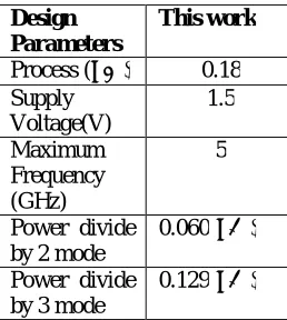
The simulations of the designs are performed using Microwind for a 0.18μM CMOS process. The simulation results show that the wide band 2/3 prescaler has the maximum operational frequency of 5 GHz with a power consumption of
0.129μW throughout the divide-by-2 and divide-by-3 modes. The projected wide band multimodulus prescaler has the
ISSN (Print) : 2320 – 3765 ISSN (Online): 2278 – 8875
I
nternational
J
ournal of
A
dvanced
R
esearch in
E
lectrical,
E
lectronics and
I
nstrumentation
E
ngineering
(A High Impact Factor, Monthly, Peer Reviewed Journal)
Website: www.ijareeie.com
Vol. 7, Issue 11, November 2018
frequency of 7.2 Gigacycle per second (simulation) with a lower power consumption throughout the divide-by-32, divide-by-33, divide-by-47 and divide-b48, respectively. Fig. 6 illustrates the characteristics of Propagation delay with respect to the width of the pMOS transistor.
Fig. 6 Characteristics of Propagation delay
TABLE I. SYNTHESIS RESULTS
Design Parameters
This work
Process (μM) 0.18 Supply
Voltage(V)
1.5
Maximum Frequency (GHz)
5
Power divide by 2 mode
0.060(μW)
Power divide by 3 mode
0.129(μW)
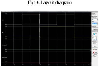
The performance of the multi modulous divider is measured infrequency bands by programmingthe counter. Fig. 7shows the measured output wave formof the multi modulous divider at associate input frequency of 2.47 GHz whereFig. 8 shows the layout ofthe multi modulous at the frequency of 5 GHz. The projected divider consumes an average power of 0.129μW. The synthesis results of proposed system have shown in table I.
ISSN (Print) : 2320 – 3765 ISSN (Online): 2278 – 8875
I
nternational
J
ournal of
A
dvanced
R
esearch in
E
lectrical,
E
lectronics and
I
nstrumentation
E
ngineering
(A High Impact Factor, Monthly, Peer Reviewed Journal)
Website: www.ijareeie.com
Vol. 7, Issue 11, November 2018
As the feature size of MOSFETs continues to shrink, a proportional downscaling within the supply voltage is necessary to keep up gate oxide dependableness. However, in thought of the sub threshold leak and also the noise margin needed by the digital integrated circuits, the scaling rate of the threshold voltage is comparatively slow compared therewith of the supply voltage. Consequently, the overdrive voltage of the transistors more and more decreases because the technology advances. It has become an inevitable trend to work the MOS devices in moderate or weak inversion for certain mixed-signal and RF integrated circuits, motivating the development of low-voltage design techniques solely for deep-sub micrometer CMOS technologies. In an RF receiver frontend, the low-noise amplifier (LNA) and also the down-conversion mixer are thought of the foremost vital building blocks. Typically, these circuits suffer from vital degradation within the RF properties, particularly for gain, noise figure, and linearity, as the transistors operate in weak inversion. to beat the restrictions on the supply voltage and also the semiconductor unit overdrive, a complementary current-reused topology has been projected for the RF frontend circuits. Using a traditional zero.18μm CMOS methodology, AN ultra-low-voltage LNA and mixer acceptable for operations with microwatt power consumption area unit realized at the 5-GHz waveband. Fig 9 and Fig. 10 shows the output wave types of voltage vs. time and voltage vs. current respectively.
Fig. 7 Output wave forms of multi modulous frequency divider
Fig. 8 Layout diagram
ISSN (Print) : 2320 – 3765 ISSN (Online): 2278 – 8875
I
nternational
J
ournal of
A
dvanced
R
esearch in
E
lectrical,
E
lectronics and
I
nstrumentation
E
ngineering
(A High Impact Factor, Monthly, Peer Reviewed Journal)
Website: www.ijareeie.com
Vol. 7, Issue 11, November 2018
Fig. 10 Voltage vs. current wave form
VI. CONCLUSION
In this paper, a wideband 2/3 or 4/5 prescaler is verified within the design of planned wide band multimodulus 32/33/47/48 or 64/65/79/80 prescaler. A multi modulous prescaler is designed with an additional multiplexer to pick out the 2/3 or 4/5 prescaler. Planned system is verified using the 0.18µm CMOS technology. Since the multimodulus 32/33/47/48 prescaler has maximum operative frequency of 5 gigahertz, the values of integrated counter will actually be programmed to divide over the total range of frequencies from one to five gigahertz with finest resolution of fifty mhz. this method will give an answer to the low power PLL synthesizers for Bluetooth, ZigBee, IEEE 802.15.4, and IEEE 802.11a/b/g LAN applications.
REFERENCES
[1] ManthenaVamshi Krishna, Graduate Student Member, IEEE, ManhAnh Do, Senior Member, IEEE, KiatSeng Yeo, ChirnChye Boon, Member,
IEEE, and Wei Meng Lim, “Design and Analysis of Ultra Low Power True Single Phase Clock CMOS 2/3 Prescaler”, IEEE TRANSACTIONS ON CIRCUITS AND SYSTEMS—I: REGULAR PAPERS, VOL. 57, NO. 1, JANUARY 2010.
[2] João Navarro, S., Jr., and Wilhelmus A. M. Van Noije, “Extended TSPC Structures With Double Input/Output Data Throughput for Gigahertz
CMOS Circuit Design”, IEEE TRANSACTIONS ON VERY LARGE SCALE INTEGRATION (VLSI) SYSTEMS, VOL. 10, NO. 3, JUNE 2002
[3] Xiao Peng Yu, Member, IEEE, ManhAnh Do, Senior Member, IEEE, Wei Meng Lim, KiatSeng Yeo, and Jian-Guo Ma, Senior Member, IEEE,
“Design and Optimization of the Extended TrueSingle-Phase Clock-Based Prescaler” IEEE TRANSACTIONS ON MICROWAVE THEORY AND TECHNIQUES, VOL. 54, NO. 11, NOVEMBER 2006.
[4] Hemapradhap N, Ajayan J “High Speed Low-Power True Single-Phase Clock Divide-by-16/17 Dual-Modulus Prescaler Using 130nm CMOS
Process With a VDD of 1.2V”, IEEE International Conference on Circuit, Power and Computing Technologies [ICCPCT], 2016 IEEE.
[5] Wenrui Zhu, Haigang Yang, TongqiangGao, Fei Liu, Tao Yin, Dandan Zhang, and Hongfeng Zhang, “A 5.8-GHz Wideband TSPC
Divide-by-16/17 Dual Modulus Prescaler”, IEEE TRANSACTIONS ON VERY LARGE SCALE INTEGRATION (VLSI) SYSTEMS, VOL. 23, NO. 1, JANUARY 2015.
[6] Song Jia, Ziyi Wang, Shilin Yan, Yuan Wang, “A Leakage Tolerant True Single-Phase Clock Dual-Modulus Prescaler Scheme”,
[7] Hamid R. Rategh, Student Member, IEEE, HiradSamavati, Student Member, IEEE, and Thomas H. Lee, Member, IEEE, “A CMOS Frequency
Synthesizer with an Injection-Locked Frequency Divider for a 5-GHz Wireless LAN Receiver” IEEE JOURNAL ON SOLID-STATE CIRCUITS, VOL. 35, NO. 5, MAY 2000
[8] Song Jia*,†, Ziyi Wang, Shilin Yan and Yuan Wang, “A true single-phase clock dual-modulus prescaler with enhanced robustness against
leakage currents”, INTERNATIONAL JOURNAL OF CIRCUIT THEORY AND APPLICATIONS Int. J. Circ. Theor. Appl. (2016)
[9] ManthenaVamshi Krishna1, Anil Jain, Nasir Abdul Quadir, Paul D. Townsend, Peter Ossieur“ A 1V 2mW 17GHz Multi-Modulus Frequency
Divider based on TSPC logic using 65nm CMOS , 978-1-4799-5696-8/14/, IEEE 2014.
[10] Mohammed Zackriya. V, Harish M Kittur, “90nm CMOS Low Power Multimodulus 32/33/39/40/47/48 Prescaler with METSPC Based Logic,
IEEE 2013 Third International Conference on Advances in Computing and Communications, 978-0-7695-5033-6/13, IEEE.
[11] AtanuChattopadhyay, Member, IEEE, and ZeljkoZilic, Senior Member, IEEE, “Flexible and Reconfigurable Mismatch-Tolerant Serial Clock
Distribution Networks”, IEEE TRANSACTIONS ON VERY LARGE SCALE INTEGRATION (VLSI) SYSTEMS, VOL. 20, NO. 3, MARCH 2012
[12] Amruta A. Kulkarni, Member IEEE and Prasad D. Khandekar, Senior Member IEEE, “Design and Implementation of Low Power Clock
Distribution Network, IEEE-International Conference On Advances In Engineering, Science And Management (ICAESM -2012) March 30, 31, 2012
[13] Xiao Peng Yu, Member, IEEE, ManhAnh Do, Senior Member, IEEE, Wei Meng Lim, KiatSeng Yeo, and Jian-Guo Ma, Senior Member, IEEE,
“Design and Optimization of the Extended True Single-Phase Clock-Based Prescaler”, IEEE TRANSACTIONS ON MICROWAVE THEORY
ISSN (Print) : 2320 – 3765 ISSN (Online): 2278 – 8875
I
nternational
J
ournal of
A
dvanced
R
esearch in
E
lectrical,
E
lectronics and
I
nstrumentation
E
ngineering
(A High Impact Factor, Monthly, Peer Reviewed Journal)
Website: www.ijareeie.com
Vol. 7, Issue 11, November 2018
[14] Nemitha B, Pradeep Kumar, “High speed, Low power N/ (N+1) prescaler using TSPC and E-TSPC: A survey” International Journal of
Advanced Research in Electrical, Electronics and Instrumentation Engineering, Vol. 3, Issue 4, April 2014.
[15] Vamshi Krishna Manthena, ManhAnh Do, ChirnChye Boon, and KiatSeng Yeo “A Low-Power Single-Phase Clock Multiband Flexible
Divider” IEEE TRANSACTIONS ON VERY LARGE SCALE INTEGRATION (VLSI) SYSTEMS, 2011 IEEE.
[16] S. Pellerano, S. Levantino, C. Samori, and A. L. Lacaita, “A 13.5-mW 5-GHz frequency synthesizer with dynamic-logic frequency divider,”
IEEE J. Solid-State Circuits, vol. 39, no. 2, pp. 378–383, Feb. 2004.
[17] J.Suganthi, N.Kumaresan, K.Anbarasi, “Design of Power Efficient divide by 2/3 Counter using E-TSPC based Flip Flops” International Journal
of Innovative Technology and Exploring Engineering (IJITEE) ISSN: 2278-3075, Volume-1, Issue-2, July 2012
[18] R.MAHESH KUMAR and PANEM.CHARAN ARUR, “A Low-Power Single-Phase Clock Multiband Flexible Divider”, International Journal
of Emerging Trends in Electrical and Electronics (IJETEE – ISSN: 2320-9569) Vol. 4, Issue. 2, June-2013.
[19] Divyashree .M, H. Venkateshkumar, “Design of a High Frequency Dual Modulus Prescaler using Efficient TSPC Flip Flop using 180nm
Technology” International Journal of Innovative Research in Science Engineering and Technology, Vol. 4, Issue 7, July 2015.
[20] Siddharth A. Koshiyar, Narendra J. Patadiya, Prof. Bharat H. Nagpara, “Design and Implementation of 2by3 Prescaler using Different Logic in
CMOS 45nm Technology”, International Journal of Innovative Research in Computer and Communication Engineering”, Vol. 3, Issue 3, March 2015.
[21] Mehul R. Soni, Nilesh D. Patel, “A Low-Power Single-Phase Dual-Modulous Prescaler”, International Journal of Innovative Research in
Computer and Communication Engineering, Vol. 3, Issue 3, March 2015
[22] João Navarro, S., Jr., and Wilhelmus A. M. Van Noije, “Extended TSPC Structures With Double Input/Output Data Throughput for Gigahertz
CMOS Circuit Design”, IEEE TRANSACTIONS ON VERY LARGE SCALE INTEGRATION (VLSI) SYSTEMS, VOL. 10, NO. 3, JUNE 2002
[23] Jiren Yuan and ChristerSvensson, “New Single clock CMOS Latches and flipflops with improved speed and power savings”, IEEE journal of
solid state circuits, vol 32, no.1, January, 1997.
[24] S Revathi, A Selvapandian, “ A Low Power 2/3 Prescaler Using Pass Transistor Logic with Integrated P&S Counter” International Journal of
VLSI and Embedded Systems, Vol 05, Article 02228, February 2014
[25] J. N. Soares, Jr. and W. A. M. Van Noije, “A 1.6-GHz dual modulus prescaler using the extended true-single-phase-clock CMOS circuit