Available online: https://edupediapublications.org/journals/index.php/IJR/ P a g e | 11
Design of Pulsed Latch Based Shift Register with Reduced
Power and Area
Ch Satya Sagar, P.G.STUDENT, Kakinada Institute of Engineering and Technology
Thulimilli Prem Bosco, Asst.Prof, Kakinada Institute of Engineering and Technology
Abstract: Power consumption and Area reduction is a major role in sequential circuit design .A
novel approach to design a pulsed latch based shift register with reduced area and power is
proposed.. In this the, conventional data Flip flops are replaced with pulsed latches to reduce area
occupation .This method solves the timing problem between pulsed latches through the use of
multiple non-overlap delayed pulsed clock signals instead of the conventional single pulsed
clock signal. In the existing system, shift register uses single pulsed clock signal for data
transition, which consumes more power. The shift register uses a small number of the pulsed
clock signals by grouping the latches to several sub shifter registers and using additional
temporary storage latches. To minimize power consumption multiple non overlap delayed pulsed
clock signal scheme is proposed for data synchronization in a multi bit shift register. The
proposed system will be carried out using Tanner T- Spice.
Keywords: flip-flop, pulsed clock, pulsed latch, shift register.
I. INTRODUCTION
Low power has emerged as a principal
theme in today’s world of electronics
industries. Powerdissipation has become an
important consideration as performance and
area for VLSI Chip design.For power
management leakage current also plays an
important role in low power VLSI designs.
Shift registers are commonly used in many
applications, such as digital filters,
communication receivers, and image
processing ICs .As the size of the image data
continues to increase due to the high
demand for high quality image data, the
word length of the shifter register increases
to process large image data in image
processing ICs. An image-extraction and
vector generation VLSI chip usesa
Available online: https://edupediapublications.org/journals/index.php/IJR/ P a g e | 12 An N-bit shift register is composed of series
connected N data flip-flops. The speed of
the flip-flop is less important than the area
and power consumption because there is no
circuit between flip-flips in the shift register.
The smallest flip-flop is suitable for the shift
register to reduce the area and power
consumption.
Fig.1: (a) Master-slave flip-flop. (b) Pulsed
latch.
Recently, pulsed latches have replaced
flip-flops in many applications, because a pulsed
latch is much smaller than a flipflop.But the
pulsed latch cannot be used in a shift register
due to the timing problem between pulsed
latches.This paper proposes a pulsed latch
based shift register with reduced area and
power. The shift register solves the timing
problem using multiple non-overlap delayed
pulsed clock signals instead of the
conventional single pulsed clock signal. The
shift register uses a small number of the
pulsed clock signals by grouping the latches
to several sub shifter registers and using
additional temporary storage latches. The
rest of the paper describes the proposed shift
register architecture and the result measures.
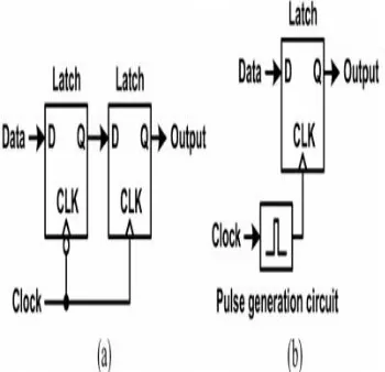
II. CONVENTIONAL SYSTEM
A master-slave flip-flop using two latches in
Fig. 1(a) can be replaced by a pulsed latch
consisting of a latch and a pulsed clock
signal in Fig. 1. All pulsed latches share the
pulse generation circuit for the pulsed clock
signal. As a result, the area and power
consumption of the pulsed latch become
almost half of those of the master-slave
flip-flop. The pulsed latch is an attractive
solution for small area and low power
consumption.
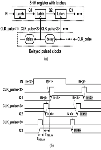
The pulsed latch cannot be used in shift
registers due to the timing problem, as
shown in Fig. 2. The shift register in Fig.
2(a) consists of several latches and a pulsed
clock signal (CLK_pulse). The operation
waveforms in Fig. 2(b) shows the timing
problem in the shifter register. The output
signal of the first latch (Q1) changes
Available online: https://edupediapublications.org/journals/index.php/IJR/ P a g e | 13 latch (IN) is constant during the clock pulse
width (TPULSE). One solution for the
timing problem is to add delay circuits
between latches,However, the delay circuits
cause large area and power occupation.
Fig.2: Shift register with latches and a
pulsed clock signal. (a) Schematic. (b)
Waveforms.
Other solution is to use multiple non-overlap
delayed pulsed clock signals, as shown in
Fig. 3(a). The delayed pulsed clock signals
are generated when a pulsed clock signal
goes through delay circuits. Each latch uses
a pulsed clock signal which is delayed from
the pulsed clock signal used in its next latch.
Therefore, each latch updates the data after
its next latch updates the data. As a result,
each latch has a constant input during its
clock pulse and no timing problem occurs
between latches. However, this solution also
requires many delay circuits.
Fig.3: Shift register with latches and delayed
pulsed clock signals. (a) Schematic. (b)
Waveforms.
III. LITERATURE SURVEY
Wenxu Zhao has proposed a new
mechanism that performs functionality of
flip-flop based on generating explicit
transparency window where the transition is
allowed. HLFF(Hybrid Latch Flip
flop)provides high performance and should
be able to toggle at 5GHz with the
difference between Q and Qbar outputs at
Available online: https://edupediapublications.org/journals/index.php/IJR/ P a g e | 14
approaches and iterating, power
consumption is calculated while running at
5GHz.All transistors are equally sized to
match timing constraints and finally power
consumption to be minimized.[1]
Vinoth,R. et al. have designed Low Power
Dual Dynamic Node Hybrid Flip-Flop. They
designed a Low power high performance
dual dynamic node hybrid flip-flop and
embedded logic module with SVL Circuit.
This design eliminates large capacitance in
the precharge node that separately drives the
output pull-up and pull-down transistors.
Their design carried out comparison of the
dual dynamic node hybrid flip-flop (DDFF),
dual dynamic node hybrid flip flop with
logic embedding capability (DDFF-ELM)
with dual dynamic node hybrid flip flop
self-controllable-voltage-level (DDFF-SVL)
logics and they obtained the best power
-delay-performance [2].
Vladimir Stojanovic and Vojin G.
Oklobdzija give a comparative study of
master slave flip flop and latches for high
performance and low power systems. They
identified three main sources of power
dissipation in latch: internal power
dissipation of the latch, local clock power
dissipation, local data power dissipation and
also measured the power dissipated by the
circuit driving the inputs of the latch to
determine the local clock and data power
dissipation [3]. Xiangyu Zhang proposed a
paper of reduced power shift register with
clock gating. He analysed that by clock
gating technique, clock to an idle portion is
disabled, thus avoiding power dissipation
due to unnecessary charging and discharging
of the unused circuit.
In this design, he used a 8-bit shift-left
register with positive-edge clock, serial In,
and serial Out. He made a comparison of
power dissipation without clock gating and
power dissipation with clock gating and
concluded that clock gating technique
significantly reduces dynamic power of shift
register [4].
V.Kavipriya and K.Sedhuramalingam
proposed a paper on Design and Analysis of
Low Power Pulse Triggered Flip-Flop .They
give a comparative analysis of a classic
explicit pulse triggered flip flop (ep-DCO),
modified hybrid latch flipflop (MHLFF)
with proposed P-FF design using signal feed
through technique. The P-FF design also
employs a static latch structure and a
conditional discharge scheme to avoid
Available online: https://edupediapublications.org/journals/index.php/IJR/ P a g e | 15 By using simple pass transistors they
achieved a better result in power
consumption [5].
Madge Deepali Harish et al. have designed a
paper on pulsed triggered flip flop for low
power applications. In this design, they
introduces a series pass transistor which
helps in reducing discharging path and made
improvement in delay. They compared
power and delay of many flip flops and
proved that pulse triggered flip flop operates
in low power [6]. Chi-Ken Tsai et al. have
proposed a pulse edge triggered latches
design in low power. The clock storage
elements using the low power technique are
realized in this paper. A Low swing
conditional capture edge-trigged
flip-flop(LSCCFF) and conditional precharged
double edge-triggered flip-flop (CPDFF) are
the two used to reduce clock power. The
comparison has been performed on the basis
of number of transistors, staticpower,
dynamic power and average clock used.
Based on this comparison, the proposed
CPDFF could save 42%~79% of the static
power and 8%~52% of the dynamic power
[7].
Byung-Do Yanghave proposed a paper on
shift register using pulsed latches.In this,
Shift register is divided into M sub shifter
registers as shown in Fig. 4(a) to reduce the
number of delayed pulsed clock signals.
Each pulsed clock signal is generated in a
clock-pulse circuit consisting a delay circuit
and an AND gate. A 4-bitsub shifter register
consists of five latches and it performs
shiftoperations with five non- -overlap
delayed pulsed clock signals are generated
by the delayed pulsed clock generator.In the
4-bit sub shift register #1, four latches store
4-bit data (Q1-Q4) and the last latch stores
1-bit temporary data (T1) which will be
stored in the first latch (Q5) of the 4-bit sub
shift register #2.
The proposed shift register reduces the
number of delayed pulsed clock signals
significantly, but it increases the number of
latches because of the additional temporary
storage latches.The sequence of the pulsed
clock signals is in the opposite order of the
five latches.The operations of the other sub
shift registers are the same as that of the sub
shift register #1 except that the first latch
receives data from the temporary storage
latch in the previous sub shift register.Fig.
4(b) shows the operation waveforms in the
Available online: https://edupediapublications.org/journals/index.php/IJR/ P a g e | 16 Fig.4: Pulsed latch based shift register (a)
Schematic. (b) Waveforms
The numbers of latches and clock-pulse
circuits change according to the word length
of the sub shift register (K).K is selected by
considering the area, power consumption,
speed
Fig.5: Delayed pulsed clock generator.
In the conventional delayed pulsed clock
circuits, the clock pulse width must be larger
than the summation of the rising and falling
times in all inverters in the delay circuits to
keep the shape of the pulsed clock.All
pulsed clock signals have almost the same
pulse skews when they arrive at the same
sub shift register. Therefore, in the same sub
shift register, the pulse skew differences
between the pulsed clock signals are very
small. The clock pulse intervals larger than
the pulse skew differences cancel out the
Available online: https://edupediapublications.org/journals/index.php/IJR/ P a g e | 17 the pulse skew differences between the
different sub shift registers do not cause any
timing problem, because two latches
connecting two sub shift registers use the
first and last pulsed clocks
IV. CONCLUSION
In this paper several architectures of pulsed
latch based shift register design is discussed.
In many architectures, the area and power
consumption are reduced by implementing
pulsed latches for shift register design
instead of flip flop. Power and area
occupation of pulsed latch based shift
register is comparatively less with rest
architectures is discussed in table 1 and 2.
The pulsed latch based shift register design
uses less number of pulsed clock signals by
merging the latches to multiple sub shift
register and also using additional temporary
storage latches. But still there is an
unwanted switching’s in the static
differential sense amp sharedpulse latch may
lead to excess dynamic power dissipation
and also area occupation. Modify the
transistor level design latch will reduce area
and power consumption in shift register
design further.
REFERENCES
[1] P. Reyes, P. Reviriego, J. A. Maestro,
and O. Ruano, “New protection techniques
against SEUs for moving average filters in a
radiation environment,” IEEE Trans. Nucl.
Sci., vol. 54, no. 4, pp. 957–964, Aug. 2007.
[2] M. Hatamian et al., “Design
considerations for gigabit ethernet 1000
base-T twisted pair transceivers,” Proc.
IEEE Custom Integr. Circuits Conf., pp.
335–342, 1998.
[3] H. Yamasaki and T. Shibata, “A
real-time image-feature-extraction and
vector-generation vlsi employing
arrayedshift-register architecture,” IEEE J. Solid-State
Circuits, vol. 42, no. 9, pp. 2046–2053, Sep.
2007.
[4] H.-S. Kim, J.-H. Yang, S.-H. Park, S.-T.
Ryu, and G.-H. Cho, “A 10-bit
column-driver IC with parasitic-insensitive iterative
charge-sharing based capacitor-string
interpolation for mobile active-matrix
LCDs,”IEEE J. Solid-State Circuits, vol. 49,
no. 3, pp. 766–782, Mar. 2014.
[5] S.-H. W. Chiang and S. Kleinfelder,
“Scaling and design of a 16-megapixel
Available online: https://edupediapublications.org/journals/index.php/IJR/ P a g e | 18 microscopy,” in Proc. IEEE Nucl. Sci.
Symp. Conf. Record (NSS/MIC), 2009, pp.
1249–1256.
[6] S. Heo, R. Krashinsky, and K. Asanovic,
“Activity-sensitive flip-flop and latch selection for reduced energy,” IEEE Trans.
Very Large Scale Integr. (VLSI) Syst., vol.
15, no. 9, pp. 1060–1064, Sep. 2007.
[7] S. Naffziger and G. Hammond, “The
implementation of the next generation 64 b
itanium microprocessor,” in IEEE Int.
Solid-State Circuits Conf. (ISSCC) Dig. Tech.
Papers, Feb. 2002, pp. 276–504.
[8] H. Partovi et al., “Flow-through latch
and edge-triggered flip-flop hybrid
elements,” IEEE Int. Solid-State Circuits
Conf. (ISSCC) Dig. Tech. Papers, pp. 138–
139, Feb. 1996.
Thulimilli Prem Bosco received
the B.tech degree in
Electronics and
Communication from Thandra
Paparaya Institute of Science
and Technology(JNTUK) and awarded M.Tech
degree in Communication systems from Sir C R
Reddy College of Engineering(A.U). He Has done
three publications. And his areas of Interest
include VLSI Design and Embedded Systems,
HDI Design, Digital Image Processing and
Communication System.
Ch Satya Sagar pursuing
M.Tech VLSID in Kakinada
Institute of Engineering
Technology, korangi. He
received Bachelor degree in
Department of Electronics and
Communication Engineering from Pragati
Engineering College