ABSTRACT
ILES, PHILIP MICHAEL. A Testbed for Technology Characterization. (Under the direction of Dr. W. Rhett Davis).
A Testbed for Technology Characterization
by
Philip Michael Iles
A thesis submitted to the Graduate Faculty of North Carolina State University
in partial fulfillment of the requirements for the Degree of
Master of Science
Electrical Engineering
Raleigh, North Carolina 2009
APPROVED BY:
_________________________ _________________________ Dr. Xun Liu Dr. Paul Franzon
DEDICATION
BIOGRAPHY
ACKNOWLEDGEMENTS
TABLE OF CONTENTS
LIST OF TABLES……….. vii
LIST OF FIGURES……… viii
CHAPTER 1 INTRODUCTION... 1
Section 1.1 Defining Characteristics of Technologies ... 1
Section 1.2 Premise of the STEEP program and the XChips... 3
Section 1.3 Tunneling Device Introduction... 4
CHAPTER 2 TEST STRUCTURES AND METHODS EXPLORED……… 7
Section 2.1 Individual Transistors ... 7
Section 2.2 Ring Oscillator ... 8
Section 2.3 Rapid Characterization of Threshold Variation... 9
Section 2.4 SRAM Bitcell... 12
Section 2.5 SRAM March Tests ... 13
CHAPTER 3 NOVEL MODIFICATIONS AND IMPROVEMENTS………. 16
Section 3.1 Rapid Threshold Characterization Improvement ... 16
Section 3.2 Usage of Rapid Characterization for On Current ... 20
CHAPTER 4 IMPLEMENTATION……….. 23
Section 4.1 Pad Restrictions ... 23
Section 4.2 SRAM Test Pattern Generator... 23
Section 4.3 90nm bulk... 24
Section 4.4 45nm SOI... 25
Section 5.1 Antenna Diodes ... 30
Section 5.2 Frequency response of Celadon probe card ... 33
Section 5.3 Layout Considerations of the Rapid DUT Cell ... 35
CHAPTER 6 RESULTS……… 39
Section 6.1 Simulations ... 39
Section 6.1.1 Ring Oscillator ... 39
Section 6.1.2 SRAM ... 41
Section 6.1.3 Threshold Voltage Variation Test Structure ... 43
Section 6.1.4 On current Variation Test Structure ... 44
Section 6.1.5 SRAM Bit-cell ... 45
Section 6.2 Measured ... 47
Section 6.2.1 Antenna Affect Diodes... 47
Section 6.2.2 Individual Transistors... 48
Section 6.2.3 Ring Oscillator ... 54
Section 6.2.4 SRAM Bit-cell ... 60
Section 6.2.5 SRAM Yield ... 62
Section 6.2.6 Rapid Threshold Variation (NMOS)... 64
Section 6.2.7 Rapid Ion Variation (NMOS)... 67
CHAPTER 7 CONCLUSIONS AND FUTURE WORK……… 69
Section 7.1 PMOS Rapid Characterization Test Structures ... 69
Section 7.2 Skill Code ... 70
Section 7.3 March Test Pattern Conversion ... 70
Section 7.4 Alternative Test Structures... 71
APPENDICIES………73
Appendix A – mtpg.pl (March Test Pattern Generator)... 74
Appendix B – x2chip.il (bubblePins procedure) ... 79
Appendix C – Simulated X2Chip Ring Oscillator Demonstrating Frequency Division... 81
LIST OF TABLES
LIST OF FIGURES
Figure 1.3.1 - Functionality of a HETT [3]... 5
Figure 2.1.1 - NMOS Transistor Structure ... 7
Figure 2.1.2 - PMOS Transistor Structure... 7
Figure 2.2.1 - Basic Ring Oscillator ... 8
Figure 2.3.1 - Rapid Vt Characterization Structure [4] ... 10
Figure 2.4.1 - 6T SRAM Bitcell ... 12
Figure 3.1.1 - Schematic of Leakage Test for Rapid Vt Structure ... 17
Figure 3.1.2 - DUT Cell with Drain T-gate for Vt Characterization... 18
Figure 3.1.3 – Simulated Leakage Reduction with Transmission Gates at Gate and Drain... 19
Figure 3.1.4 - NAND Enable Scheme for DUT Cell for Rapid Vt Characterization ... 20
Figure 3.2.1 - Rapid Ion Variation Test Structure ... 21
Figure 4.4.1 - SRAM Muxing Approach ... 26
Figure 4.4.2 - Single Transistor with no ACLV Gate ... 27
Figure 4.4.3 - Single Transistor with ACLV Gate on both sides ... 27
Figure 4.4.4 - Single Transistor with ACLV at 2x Poly Pitch... 28
Figure 4.4.5 - Single Transistor Abutted to Transistors with ACLV... 28
Figure 4.4.6 - Single Transistor with Multi-finger Devices on each side ... 29
Figure 4.4.7 - Single Transistor surrounded by Single-finger Devices... 29
Figure 5.1.1 - Antenna Diode Failure... 31
Figure 5.1.2 - Antenna Rule Fix ... 32
Figure 5.1.3 - Antenna Diode Equivalent Schematic ... 33
Figure 5.2.1 - XChip Ring Oscillator Structure ... 34
Figure 5.2.2 - X2Chip Ring Oscillator Structure ... 35
Figure 6.1.1 - XChip Ring Oscillator Simulations – Vdd from 0.5 to 1.0V ... 40
Figure 6.1.2 - X2Chip Ring Oscillator Core Simulations – Vdd from 0.5 to 1.0V ... 41
Figure 6.1.3 - X2Chip Muxed-SRAM Validation Simulation - Write... 42
Figure 6.1.4 - X2Chip Muxed-SRAM Validation Simulation – Read ... 42
Figure 6.1.5 – Simulated Accuracy of Leakage-Reduced Vt Variation Structure... 43
Figure 6.1.6 - Rapid Ion Variation Simulation ... 45
Figure 6.1.7 - Read Noise Margin Simulation ... 46
Figure 6.2.1 - Measured Antenna Diode Leakage... 47
Figure 6.2.2 – Measured XChip NOMS Ion as a function of Gate Length... 49
Figure 6.2.3 – Measured XChip NMOS Ioff as a function of Gate Length ... 50
Figure 6.2.4 – Measured XChip NMOS Ion/Ioff as a function of Gate Length ... 51
Figure 6.2.5 – Measured XChip NMOS Ion/Ioff as a function of Supply Voltage... 52
Figure 6.2.6 – Measured XChip NMOS Subthreshold Slope as a function of Gate Length ... 53
Figure 6.2.7 – Measured XChip NMOS Subthreshold Slope as a function of Supply voltage... 54
Figure 6.2.8 - Ring Oscillator at Vdd = 1.0 V... 56
Figure 6.2.9 - Ring Oscillator at Vdd = 0.7 V... 57
Figure 6.2.10 - Ring Oscillator Operating at Vdd = 0.5 V ... 57
Figure 6.2.11 - Ring Oscillator at Vdd = 0.25 V ... 58
Figure 6.2.12 - Measured Gate Delay of XChip Ring Oscillator ... 59
Figure 6.2.13 – Measured Current Consumption of Ring Oscillators ... 60
Figure 6.2.14 – Measured Read Margin of Custom Bitcell on XChip - Vdd from 0.5 V to 1.0 V... 61
Figure 6.2.16 – Measured Leakage through Bitcell ... 62
Figure 6.2.17 - Measured NMOS Treshold Variation (mean) ... 65
Figure 6.2.18 – Measured NMOS Threshold Variation (RMS)... 66
Chapter 1
Introduction
The physical limitations of traditional fabrication techniques are not many more generations away. Photolithography engineers have bought some time by developing lithography techniques that manipulate light in such a way that devices smaller than the wavelength of the light used to expose the silicon can be created. However, it has become apparent that a new type of device must be designed if engineers are to continue to push the limits of transistors. Tunneling transistors, referred to as TFETs by some, seem to be proving themselves worthy of the becoming the future de facto device. With the advancement of TFET device technology, a set of metrics must be established to quantify the improvement over current state-of-the-art technologies. This work discusses key metrics that help to define the advancement of TFET technology and provides discussion and implementation of test structures that can be used to measure these metrics.
Section 1.1
Defining Characteristics of Technologies
Current consumption, both on- and off-state, or leakage, of a device is critical to fully characterize. As technologies have shrunk, the leakage of a device has become increasingly problematic. Methods, such as body biasing, to reduce the leakage through a device in a sleep state are under constant development in existing technologies. However, the methods used to reduce the leakage of a circuit generally have negative impacts on the overall design of the circuit. As with the example of body biasing, a large area increase is observed when an extra body contact is necessary for each device. TFETs provide hope that the on and off state current consumption of a device can be dramatically improved without this necessary overhead in current technologies.
The next characteristic, device variation, has become an increasingly interesting topic as feature sizes have reduced to less than the wavelength of the light used in traditional lithography. Because of this, among other reasons, the device to device process variation has become more and more significant. Since the variation has become greater as technology shrinks, it is important to understand how much variation should be expected in order to accurately simulate the behavior of a circuit. For the purposes of this work, the variations in threshold voltage and on-state current are the primary focus of device to device variation.
voltage than traditional transistors and thus cannot necessarily be expected to perform to the same standards. This leads to one of the issues in comparing two strikingly different devices. Though the speed of a new TFET needs to be fast enough to “compete” with its traditional FET counterpart, a designer must take into consideration the potentially enormous savings in power consumption as it relates to the reduction in performance. However the comparison is quantified, the importance of characterizing the speed of a device is unquestionable.
Lastly, almost no complex digital system is complete without some sort of storage mechanism. In the majority of cases, this temporary storage exists in the form of an SRAM. Not only must the SRAM be fast, but it must also be reliable. Measuring the yield of an SRAM is vital considering their ubiquitous use in so many applications today. Due to the extensive use of SRAMs in many complex designs, the power consumption is also an important metric to measure of an SRAM. Arguably, the most important power metric related to an SRAM is its leakage current. Considering the sheer number of devices in a bit-cell array itself, the impact of reducing the overall leakage of each device becomes more and more significant.
Section 1.2
Premise of the STEEP program and the XChips
All of these attributes lead up to the fundamental characteristics of interest of the STEEP program. The STEEP program [1] is a DARPA initiative for investigating S
determine the validity of the development of a new type of transistor, the specifications of current technologies should be investigated as a comparison for these new devices. This work focuses on the design and development of two chips to provide a baseline for these comparisons, referred to hereafter as XChip and X2Chip, and collectively, XChips. XChip, the first of two, was fabricated in a 90nm bulk process. The X2Chip is an improvement on the first and was developed in a 45nm SOI technology. As of the writing of this document, the X2Chip is not available for testing.
The test structures implemented in these chips provide insight into the intrinsic characteristics of the technologies in which they are implemented. Establishing a baseline of the performance of current state-of-the-art devices provides metrics to measure the success of newly developed TFET devices. Each of the test structures mentioned in the next chapter will establish a data point in at least one of the areas of interest. If the test structures are similarly implemented in any technology, a reasonable comparison can be made through the same testing methodologies.
Section 1.3
Tunneling Device Introduction
manifestation of a tunneling device that has been developed in conjunction with the STEEP program.
HETTs function in a way similar to traditional MOSFETs where by a voltage induced at the gate allows current to flow. However for HETTs, and more generally TFETs, it is not that a channel has formed allowing for the electrons to move from one node to another, rather, the gate bias has reduced the semiconductor bandgap allowing electrons to more easily move from the valence band to the conduction band. The below figure from [3] illustrates the on and off state of a HETT device.
Figure 1.3.1 - Functionality of a HETT [3]
Chapter 2
Test Structures and Methods Explored
Section 2.1
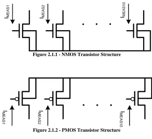
Individual Transistors
This basic intention of the XChips was to provide very the most fundamental metrics of individual devices. Thus, to ensure that this goal was met, both N- and P- type transistors were individually padded out. In order to maximize the number of devices that could be tested with the pad set and area limitations, nodes of the devices were tied together. The two illustrations below depict the schematic arrangement of the individual transistor probe sites.
Figure 2.1.1 - NMOS Transistor Structure
Section 2.2
Ring Oscillator
The most fundamental logic building block used in digital design today is the inverter. Not only do so many logic operations require both the positive logic as well as its complement (for example: muxing) but this simple device is also the basis of distributing clocks throughout an entire chip. The inverter, in odd numbers, also serves as the basis for a ring oscillator. Because the inverter is used so widely it has become a unit of comparison for a number of defining characteristics of technologies. For this reason, we can use the current and power consumption of an inverter to understand the power consumption of a particular technology. By creating a simple ring oscillator in any technology, the current consumed by each inverter in the chain can be determined and thus a known value of power consumption for this device can be observed. With a common implementation of a ring oscillator being enabled by a NAND gate, when the ring oscillator is disabled, the static power consumption can also be measured since the ring oscillator is no longer oscillating.
Figure 2.2.1 - Basic Ring Oscillator
devices can be extrapolated. Assuming the number of inverters is much, much larger than the single NAND used for the enabling of the ring oscillator, the difference between the average delays seen through the inverters compared to the single NAND can be ignored thus providing an accurate measure of delay through the inverter. Furthermore, if the ratio of N to P devices in the inverter is known, the general “strength” of each of these devices can be measured, providing even more insight into the behavior of the individual device.
Section 2.3
Rapid Characterization of Threshold Variation
Another characteristic of a technology that warrants thorough exploration is the process variations that impact circuit design, particularly threshold voltage variation. Especially when a technology is in its infancy, it is crucial for the foundry to be able to provide the most accurate models of their devices to allow the design engineers to accurately simulate the behavior of their circuits. The ability to create statistical models of device parameters allows the foundry to improve the simulation capabilities and thus improving yield of the designer’s circuits due to increased understanding of the behavior of a circuit.
operation relies upon the drain voltage to vary in such a way to keep the current through the device constant regardless of the change in threshold variation.
Figure 2.3.1 - Rapid Vt Characterization Structure [4]
symbol at the top of the circuit as suggested in the author’s original circuit diagram is a bit misleading. In order observe the expected behavior of the circuit, these gates should actually be considered transmission gates, the same as seen at the bottom of the circuit. By enabling one row and one column, one particular device in the array becomes the device-under-test (DUT). The current is forced to flow in one direction from the opamp through the DUT and along the common source node for the row then out of the circuit to the current source. This path is illustrated by arrows in the above figure.
Since the current is forced in one direction only, both the drain and source voltages can be sensed without the worry of parasitic IR drop. The sensed voltage of the drain and the inverted sensed voltage of the source (through the source follower at the input of the opamp) provide the necessary input to the opamp to modify the output voltage in order to maintain a constant current through a selected device.
As each device of the array is selected, VGS can be measured. As proven in [4], VGS varies directly with Vth so long as the current is kept constant. This is due to the fact that the current is dependent on the quantity of (VGS – Vth) and not VGS or Vth separately. Therefore the variation in the threshold voltage directly correlates to the variation in VGS and thus the method of measuring Vth variation for this circuit.
RMS value as the first standard deviation of the device mismatch. This approach has been used with the Vt variation structure as mentioned in [5].
Section 2.4
SRAM Bitcell
Any technology that is used to implement complex digital systems must provide reliable, and preferably fast, SRAMs. But before an SRAM can be designed, the bitcell itself must be fully understood in order to properly design portions of the SRAM such as the pre-charge circuitry and the sense amplifiers. Two key metrics that can be quantified to help in this design are the read and write noise margins of the bitcell as discussed in [6]. For the purposes of this work, a typical 6-T SRAM bitcell, below, is used as a test device.
Figure 2.4.1 - 6T SRAM Bitcell
increase in current through the BL node indicates the read noise margin of the cell. Similarly, the bit line write margin can be identified by setting BL, VCELL, and WL to VDD. Then, BL_b is swept from Vss to Vdd and the point at which the current through the BL node abruptly changes indicates the write noise margin [6]. Another important measure of the performance of the bitcell is its leakage current. In order to measure this, WL is set to Vss while BL and BL_b are set to Vdd, somewhat simulating a pre-charge, and VCELL is swept from Vss to Vdd. These three measurements of the bitcell help to provide necessary information for designers to develop robust SRAMs.
Section 2.5
SRAM March Tests
Beyond understanding the behavior of the bitcell itself, it is crucial to also be able to characterize the effective yield of a particular technology. SRAMs lend themselves very well to yield tests considering the extreme density normally observed within the bitcell array. In addition, the uniformity of the array itself helps to mitigate systematic variation observed between devices. For the purposes of this work, a march test will be used to measure the effective yield of an SRAM.
coverage. It should be noted that the algorithm chosen is independent of the hardware unless the march test algorithm is actually implemented on-chip. In this work, the control logic is located off-chip and thus any march test pattern can be used to measure the yield of the SRAM.
A march test consists of several “march elements” that are chained together in a specified order. Obviously there are two operations permitted on a memory: read (r) and write (w). Secondly, in stride with the binary operation of traditional digital electronics, there are only two values that are permitted to be stored in a memory cell: 0 or 1. The last part of the march element is the order in which the operation should be performed in relation to other words in the structure: u (up - ↑), d(down - ↓), ud(up or down - ↕). In [7] the arrow notation is used while in this work u, d, and ud are used as they are the syntax used for the pattern generation script written for this project.
The first, and simplest, algorithm discussed is the MATS+ algorithm. The algorithm, written in the original format looks like:
↕{w0}; ↑{r0,w1}; ↓{r1,w0}
the address range and attempt to read the 1 from each word followed by writing a 0. This simple notation can very easy describe much more complex algorithms, such as the March C algorithm (which should easily be deciphered based on the previous example):
ud{w0}; u{r0,w1}; u{r1,w0}; d{r0,w1}; d{r1,w0}; ud{r0}
Chapter 3
Novel Modifications and Improvements
Section 3.1
Rapid Threshold Characterization Improvement
With the continued reduction of transistor sizes accompanied by the increase in leakage current, improvements may be necessary upon the rapid characterization test structure for future use. In order to continue to use this structure as these problems become more significant, this work proposes an approach for reducing the amount of leakage seen in the rapid characterization structure.
Figure 3.1.1 - Schematic of Leakage Test for Rapid Vt Structure
column, enabling the transmission gate per row effectively reduces the amount of leakage observed in a column of devices.
Figure 3.1.2 - DUT Cell with Drain T-gate for Vt Characterization
Rapid Vt Leakage Reduction 0% 2% 4% 6% 8% 10% 12% 14% 16% 18% 20%
0.00E+00 1.00E-06 2.00E-06 3.00E-06 4.00E-06 5.00E-06 6.00E-06 Transmission Gate Width (um)
lea kag e r ed u ct io n
Figure 3.1.3 – Simulated Leakage Reduction with Transmission Gates at Gate and Drain
Figure 3.1.4 - NAND Enable Scheme for DUT Cell for Rapid Vt Characterization
The trade off between enabling schemes is obviously area. As logic is added to each of the DUT cells, the size will increase. However, it should be noted the transistor sizes needed for the NAND and inverter can be minimum size as high-performance is unnecessary for this test structure due to the relatively slow clocking speed.
Section 3.2
Usage of Rapid Characterization for On Current
to ground instead of a current source, the same procedure used to measure threshold variation can be used to measure the on-state current variation. The following figure shows the topology of this test structure.
Figure 3.2.1 - Rapid Ion Variation Test Structure
Chapter 4
Implementation
As with any project, design trade-offs must be weighed to determine the most effective solution to the problem at hand. The development of the XChips was no different. In this section the design decisions and actual implementations in each chip are discussed.
Section 4.1
Pad Restrictions
The first challenge of the project was pad restrictions. The testing goal of the STEEP program was to design test structures and methodologies that can be applied by each development team with minimal changes. Therefore it was required that each team use the same testing equipment, namely a common probe card, thus limiting the number of pads to 25. In addition the pad size was also required to be the same among all test groups to ensure the probe card could be used to measure results in each implementation. Because the pads were so large and the limit of 25 pads per test structure was imposed, the size of the layouts was actually dominated by the sheer number of pads rather than the circuits themselves.
Section 4.2
SRAM Test Pattern Generator
size of the SRAM (data and address sizes) and the algorithm of the march test pattern desired to be performed and creates a test pattern to perform the desired algorithm. This code can be seen in the appendix. The MTPG generates a generic output that indicates the operation, address, and data instruction to be exercised upon the SRAM. This is not enough to be able to run the test. Each team must take the generated pattern and convert it into a format that the available test equipment can understand. The MTPG output can be in decimal, hexadecimal, or binary, providing ample flexibility for an easy conversion between the generic output and the input for the appropriate equipment.
Section 4.3
90nm bulk
The first XChip was manufactured in a 90nm bulk technology. The size for the first chip was rather large, nearly a 5mm x 5mm die. This large die allowed for plenty of room for many padsets. Because of this there were 12 pad sets for individual transistor probing, 6 for N- and 6 for P-type devices. Between each device set, the dimensions of the transistors were varied.
satisfactory considering the restrictions and that XChip was only required to meet Phase I goals.
The SRAM bitcell, as mentioned earlier, was instantiated on its own allowing for the noise margin tests to be conducted on a single bitcell. Due to time constrains and license agreement issues, an official dense SRAM bitcell layout was not available in time for tapeout. However a custom layout of the same dimension devices was created to serve as a proof of concept for the measurement methodology.
Section 4.4
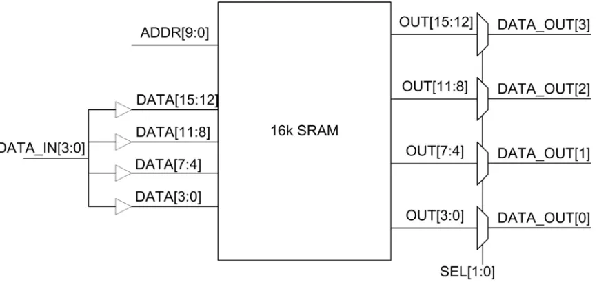
45nm SOI
Figure 4.4.1 - SRAM Muxing Approach
Fortunately, an official dense SRAM bitcell was acquired for the tapeout of X2Chip. The key improvements over the XChip are that this SRAM bitcell is both state-of-the-art industry standard and is surrounded by other bitcells just as it would be in a real SRAM bitcell array. The significance of both of these changes is to hopefully reproduce measurement values that are more similar to the behavior of a bitcell as it would operate in an SRAM. Since bitcells are designed to be tiled into a very large, dense array, the wiring for the bitlines and wordlines is built into the cell itself and the overlapping of the bitcells creates the wiring among them. For the purposes of this test, the connectivity had to be removed from surrounding the bitcells in order to isolate just one bitcell for test.
reasonable task to accomplish. As mentioned throughout this work, the concern of variation plays an important role in the characterization of a technology; therefore, individual transistor sizes with varying layouts were created to measure how this will affect the basic characteristics of the transistors. Below are images of the six different layouts of individual transistor sites for the X2Chip with a briefly descriptive caption indicating the physical variation. The layouts chosen for this are based on the study performed in [8].
Figure 4.4.2 - Single Transistor with no ACLV Gate
Figure 4.4.4 - Single Transistor with ACLV at 2x Poly Pitch
Figure 4.4.6 - Single Transistor with Multi-finger Devices on each side
Chapter 5
Lessons Learned
As with any design process, not all aspects of the design can be foreseen and planned for from the first phase of the design process. This section recounts several lessons learned at later stages in the development of the XChips and provides commentary of their impacts on the two designs.
Section 5.1
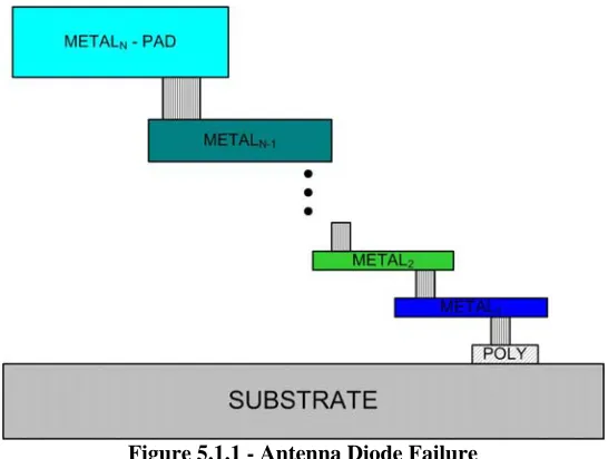
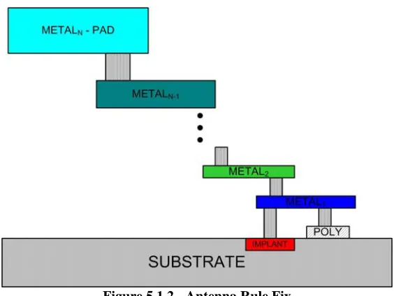
Antenna Diodes
The antenna design rule checks calculate the total area of metal connected to each polysilicon shape. When this ratio breaches a particular threshold a violation is flagged. In the general design of circuits, this ratio is rarely reached. However, once the metal of the pad and corresponding vias are taken into consideration at the chip level, this becomes a prevalent issue. The following depicts an antenna rule violation that was commonly observed.
Figure 5.1.1 - Antenna Diode Failure
diode in parallel to the gate in question the antenna rules are satisfied thus avoiding the potential destruction of a gate.
Figure 5.1.2 - Antenna Rule Fix
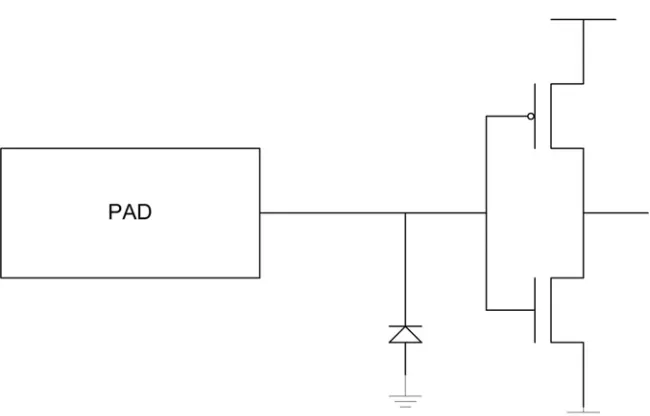
Antenna diodes are essentially reverse biased diodes that are used in parallel with any net that exhibits this violation. However, they have no schematic representation; i.e., LVS does not recognize an antenna diode as a device which needs a schematic counterpart. To some degree an antenna diode can be thought of in the same manner as ESD protection on a chip, with the difference being that it is intended to safeguard the chip during fabrication not packaging or use.
design, all unused pads had an antenna diode attached so that the I-V characteristics of the diode could be measured and its leakage taken into consideration should it prove to be significant enough.
Figure 5.1.3 - Antenna Diode Equivalent Schematic
Section 5.2
Frequency response of Celadon probe card
As an example, testing the frequency output of the ring oscillators required using manual probes landed on the probe pads instead of utilizing the probe card which lands all pads at once. This proved to be a rather complex task as five probes were required to monitor one ring oscillator. The process of setting up the probes and ensuring proper connectivity can take upwards of an hour. Since the goal was to measure the power consumption and frequency of small transistors, larger output buffers had to be created to give enough power to the drivers to get off-chip. However, this required that the buffers be on a separate power rail than the ring oscillator core, thus introducing the fifth pin. The total pin out was: vdd_core, vdd_buf, enable, out, and gnd as seen in the below figure.
Figure 5.2.1 - XChip Ring Oscillator Structure
create a core ring oscillator and use flip-flops to perform frequency division. Though some accuracy could be lost by this method due to intrinsic behaviors of the flip-flop, this approach provides enough accuracy when considering it greatly improves the testing procedures since all ring oscillators on a pad set can be tested by landing the probe card only once on the chip.
Figure 5.2.2 - X2Chip Ring Oscillator Structure
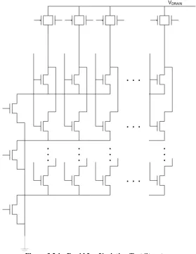
Section 5.3
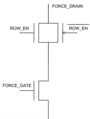
Layout Considerations of the Rapid DUT Cell
Figure 5.3.1 - DUT Cell from XChip
wire. This improved approach of the DUT cell allowed an order of magnitude more DUT cells to be instantiated in the X2Chip (1024) in comparison to the XChip (100).
Figure 5.3.2 – Wiring from DUT Cell of X2Chip
Chapter 6
Results
As with any design process, the verification of the final product and the comparisons between the simulated results and the actual measured results are of the utmost importance. In the following sections, both simulations of each design and measured results of the XChip are presented.
Section 6.1
Simulations
Section 6.1.1 Ring Oscillator
Figure 6.1.1 - XChip Ring Oscillator Simulations – Vdd from 0.5 to 1.0V
Figure 6.1.2 - X2Chip Ring Oscillator Core Simulations – Vdd from 0.5 to 1.0V
Section 6.1.2 SRAM
the SRAM implemented for the X2Chip since the data in was tied together and the data out was muxed. The test bench of this simulation can be found in the appendix.
Figure 6.1.3 - X2Chip Muxed-SRAM Validation Simulation - Write
Figure 6.1.4 - X2Chip Muxed-SRAM Validation Simulation – Read
Section 6.1.3 Threshold Voltage Variation Test Structure
The rapid characterization test structure has been rigorously tested in [4] and thus the proof of the overall circuit functionality is omitted from this work. However, with the modifications to reduce leakage, confirmation of a high degree of correlation between expected and simulated values is necessary. Below is a plot showing the how variations in Vt track against the perceived Vt as measured through the variation structure for the the XChip and X2Chip. In order to perform this simulated variation, a threshold adder parameter in the implemented technology kits was utilized to specify a particular threshold value. -0.025 -0.02 -0.015 -0.01 -0.005 0 0.005 0.01 0.015 0.02 0.025
-0.03 -0.02 -0.01 0 0.01 0.02 0.03
Expected Vt Variation (V)
S im ul a te d V t V a ri a ti on ( V ) XChip X2Chip Reference Line
The following table shows a brief statistical analysis of the error observed in the improved version of the rapid Vt variation structure. As can be seen by the table, the X2Chip implementation was a substantial improvement over the initial implementation.
XChip X2Chip average 4.598% 1.524% max 8.550% 1.850% min 0.333% 1.250% std dev 1.590% 0.192%
Table 6-1 – Simulated Error Margin of Vt Test Structures
Section 6.1.4 On current Variation Test Structure
Figure 6.1.6 - Rapid Ion Variation Simulation
Section 6.1.5 SRAM Bit-cell
The first metric shown is the read noise margin. Interestingly, even though the nominal operating voltage of both technologies is 1.0V, the read noise margin does not exhibit the same dramatic increase in current through the bit line nodes as is seen when the cell operates at 0.9V.
Figure 6.1.7 - Read Noise Margin Simulation
Section 6.2
Measured
As of the writing of this paper, the XChip is the only available chip to perform verification on. The X2Chip will not be available for some time due to standard fabrication turn around time. The following sections present the portions of the XChip that have been measured. All values presented in this section are viable data points to compare the characteristics of one technology to another.
Section 6.2.1 Antenna Affect Diodes
An I-V characteristic curve of each antenna diode in the design is shown below.
XChip Measured Antenna Diode Leakage
1E-15 1E-14 1E-13 1E-12 1E-11 1E-10 1E-09 1E-08 1E-07 1E-06 1E-05 0.0001 0.001 0.01 0.1 1
-0.5 -0.25 0 0.25 0.5 0.75 1
Vd (V) Ile a k ( A )
The above figure shows that under normal operating voltages, the leakage through any given antenna diode is in the range of 10’s of pA or less. These measurements prove that the leakage through any given antenna diode in the XChips has a negligible impact on the accuracy of the measurements since the test structures themselves generally consume current in the uA range.
Section 6.2.2 Individual Transistors
Since individual transistor characterization was the primary focus of Phase I of the STEEP program, providing analysis of the performance of individual transistors in the metrics defined by the program was of the highest priority. In order to analyze the basic characteristics of Ion, Ioff, and subthreshold slope, a parameter analyzer designed to perform these sorts of tests was utilized. The following plots in this section show the overall measured trends of the 90 nm bulk technology in which the XChip was fabricated. For the purposes of this work, only one die was measured. Each length data point is defined as the average of the 10 devices for each transistor dimension on the tested die.
XChip NMOS Ion
0 100 200 300 400 500 600 700
0.07 0.08 0.09 0.1 0.11 0.12 0.13
Gate Length (um)
Id
(
u
A
/u
m
)
Ion @ 0.5 V
Ion @ 0.75 V
Ion @ 1.0 V
XChip NMOS Ioff
0 0.001 0.002 0.003 0.004 0.005 0.006
0.07 0.08 0.09 0.1 0.11 0.12 0.13
Gate Length (um)
Il
eak (
u
A
/u
m
)
Ioff @ 0.5 V
Ioff @ 0.75 V
Ioff @ 1.0 V
Figure 6.2.3 – Measured XChip NMOS Ioff as a function of Gate Length
XChip NMOS Ion/Ioff
0 50000 100000 150000 200000 250000 300000 350000 400000 450000 500000
0.07 0.08 0.09 0.1 0.11 0.12 0.13
Gate Length (um)
Ion/
If
f Ion/Ioff @ 0.5 V
Ion/Ioff @ 0.75 V
Ion/Ioff @ 1.0 V
Figure 6.2.4 – Measured XChip NMOS Ion/Ioff as a function of Gate Length
XChip NMOS Ion/Ioff 0 50000 100000 150000 200000 250000 300000 350000 400000 450000 500000
0.4 0.5 0.6 0.7 0.8 0.9 1 1.1
Vdd (V)
Io
n
/Io
ff
L = 0.08um L = 0.09um
L = 0.1um L = 0.11um
L = 0.12um
Figure 6.2.5 – Measured XChip NMOS Ion/Ioff as a function of Supply Voltage
Subthreshold Slope
72 73 74 75 76 77 78 79 80 81
0.07 0.08 0.09 0.1 0.11 0.12 0.13
Gate Length (um)
S (m
V/d
e
c
)
Vdd @ 0.5 V
Vdd @ 0.75 V
Vdd @ 1.0 V
XChip NMOS Subtreshold Slope 72 73 74 75 76 77 78 79 80 81
0.4 0.6 0.8 1
Vdd (V) S ( m V/d e c
) L = 0.08um
L = 0.09um
L = 0.1um L = 0.11um
L = 0.12um
Figure 6.2.7 – Measured XChip NMOS Subthreshold Slope as a function of Supply voltage
Again, both of these figures illustrate the general trends observed with standard MOSFET devices. This plots show that regardless of the supply voltage chosen for a particular device, the subthreshold slope is closely dependent on the length of the transistor under test.
Section 6.2.3 Ring Oscillator
XChip does not always perform proper callback routines to calculate attributes of a transistor such as area and perimeter of source and drain regions unless certain transistor configurations are preselected. The second attributing factor is the standard inaccuracy of schematic based simulations. However, the measurements backup the trend of reduced operating frequency as the supply voltage is reduced. At a nominal supply voltage of 1.0V, the ring oscillator is shown to operate at approximately 30.5 MHz with a current consumption of approximately 27uA.
With 420 inverters and 1 NAND, the average power consumption of each inverting stage of the ring oscillator at nominal supply voltage is approximately 65nW. Based on the dimensions of the transistors and an observed nearly 50% duty cycle, it stands to reason that a beta ratio of approximately 1.7 in this technology produces an inverter equally capable of driving either direction.
Figure 6.2.9 - Ring Oscillator at Vdd = 0.7 V
Figure 6.2.11 - Ring Oscillator at Vdd = 0.25 V
Gate Delay
1.00E-09 1.00E-08 1.00E-07 1.00E-06 1.00E-05 1.00E-04
0.25 0.35 0.45 0.55 0.65 0.75 0.85 0.95 1.05
Vdd (V)
tp
0 (s/
u
m
)
Figure 6.2.12 - Measured Gate Delay of XChip Ring Oscillator
Current Consumption 0.00E+00 5.00E-06 1.00E-05 1.50E-05 2.00E-05 2.50E-05 3.00E-05
0.0 0.2 0.4 0.6 0.8 1.0 1.2
Vdd (V) C u rr e n t (A) 0.00E+00 2.00E+01 4.00E+01 6.00E+01 8.00E+01 1.00E+02 1.20E+02 Io n /I o ff r a ti o Average On Average Off Ion/Ioff
Figure 6.2.13 – Measured Current Consumption of Ring Oscillators
Section 6.2.4 SRAM Bit-cell
data (sudden “dip” for the 0.9V and sudden rise then return for the 1.0V) could also be explained by the use of a custom bitcell. However, as of the time of this writing no data exists to explain what is happening at these points of interest.
Read Noise Margin (VDD 0.5 to 1.0V)
0.00E+00 5.00E-06 1.00E-05 1.50E-05 2.00E-05 2.50E-05 3.00E-05 3.50E-05 4.00E-05
0 0.2 0.4 0.6 0.8 1
Vcell (V)
I_
b
itl
in
e
(A
)
VDD=0.5 VDD=0.6 VDD=0.7 VDD=0.8 VDD=0.9 VDD=1.0 (nom)
Figure 6.2.14 – Measured Read Margin of Custom Bitcell on XChip - Vdd from 0.5 V to 1.0 V
The final important metric identified in this SRAM bitcell is the leakage observed when the bitcell is in a hold state. As discussed earlier, the word line is unasserted and the internal VCELL is swept from 0 to 1.0 V. As observed in other aspects of the measurements, the positive correlation between leakage current and supply voltage hold true for the bitcell as well.
0.00E+00 2.00E-10 4.00E-10 6.00E-10 8.00E-10 1.00E-09 1.20E-09
0 0.2 0.4 0.6 0.8 1 1.2
Vcell (V)
Ile
a
k
(
A
)
Figure 6.2.15 – Measured Leakage through Bitcell
Section 6.2.5 SRAM Yield
work. The number of bit failures for each element in the march test as well as the total number of failures can been seen in the following table. The highlighted portion of the table indicates SRAMs that were ignored for the purposes of the calculations in the table. These three SRAMs suffered some form of catastrophic failure in that their failure rate well exceeded normal values. These failures could be result of a failure within the SRAM itself, or could indicate a problem during the actual test and data gathering.
March Element
1 2 3 4 5
Padset r0,w1 r1,w0 r0,w1 r1,w0 r0 Total
AA 35 0 10 0 0 45
AB 22 0 22 0 0 44
AC 0 0 10 0 0 10
AD 21 0 10 0 0 31
AE 32 0 0 0 0 32
AF 32 0 60 0 0 92
AG 20 0 10 0 0 30
AH 10 0 33 0 0 43
O 1766 29 179 0 0
P 2576 4518 758 2708 75
Q 2540 2747 2521 2557 38
R 0 0 52 0 0 52
S 10 0 40 0 0 50
T 10 0 38 0 0 48
U 36 0 53 0 0 89
V 82 15 20 0 0 117
W 0 0 10 0 0 10
X 0 5 10 0 0 15
Y 40 0 60 0 1 101
Z 23 0 33 0 0 56
Total 373 20 471 0 1 865
Total% 0.429% 0.023% 0.541% 0.000% 0.001% 0.199%
As can be seen in the above table, when the SRAMs are generated with no redundancy or error correction, yield can be severely impacted. A failure of 865 bits out of 20k bits is not a trivial failure rate for any system requiring hardened circuitry for completely reliable performance.
Section 6.2.6 Rapid Threshold Variation (NMOS)
Figure 6.2.16 - Measured NMOS Treshold Variation (mean)
Figure 6.2.17 – Measured NMOS Threshold Variation (RMS)
behaves. In AC coupling, essentially a capacitor is put in series with the signal to be measured and the DC value at any point in time tends to drift to 0V. Because of this, all steady values measured at each device actually drift to 0 and thus reduce the RMS value and produce the error in the measurements. This error is due to the limitation of the equipment used and not an error in the use of RMS value as the standard deviation. The true standard deviation as measured from the DC coupled waveform was calculated through a spreadsheet to be 14.076mV. The value observed in a 65nm SOI technology in [4] was 19.2mV. If the assumption is that variation worsens as device dimensions decrease, then the values observed on the XChip seem to fall in line with expectations.
Section 6.2.7 Rapid Ion Variation (NMOS)
Figure 6.2.18 - Measured NMOS Ion Variation
Chapter 7
Conclusions and Future Work
The collection of test structures implemented on the XChip and X2Chip are shown in this work to provide adequate characterization of the performance of a technology node to perform comparisons among different technologies. However, as with any product of engineering, prospective improvements always exist; this final chapter discusses a few aspects of improvement that could be readily implemented into future version of such a testbed provided the time and resources are available to do so.
Section 7.1
PMOS Rapid Characterization Test Structures
Section 7.2
Skill Code
One portion of the project that could benefit from further work is the skill code that was used to create the pins of the tiled DUT cell array layout. This code doesn’t take into consideration pins that are internally connect. For instance, the feed through path of the control logic flip-flops flows from one flip-flop to the next as well as out to the device array. In this situation a pin exists both at the point where the flip-flop drives out to the array as well as the internal connection between the flip flops. If left as is, this layout will fail LVS. For the use in the X2Chip, the clean up required to fix this problem was insignificant and merely a brief annoyance. More work could be used to help define a function that creates pins based on more specific conditions. Though out of the scope of this work, developing an entire library of skill functions used to automate certain portions of VLSI design could prove incredibly useful for a wide range of projects.
Section 7.3
March Test Pattern Conversion
Section 7.4
Alternative Test Structures
There are two particular test structures of interest that, if implemented, could provide a larger sample of data to be analyzed for characterization purposes. The first is a ring oscillator structure discussed in [8] where an array of ring oscillators is created whereby each ring oscillator in the array can be individually enabled. If particular layout variations of devices wanted to be explored, creating a ring oscillator for each variant under exploration in the array would provide an excellent measure of exploring many variation impacts on frequency and power.
REFERENCES
[1] BAA 07-26: Steep-Subthreshold-Slope Transistors for Electronics with Extremely-Low-Power. http://www.darpa.mil/mto/solicitations/baa07-26/index.html
[2] W. G. Vandenberghe et al. “Analytical Model for a Tunnel Field-Effect Transistor”, MELECON, 2008.
[3] D. Kim et al. “Low Power Circuit Design Based on Heterjunction Tunneling Transistors (HETTs)”, ISLPED, 2009.
[4] K. Agarwal, S. Nassif, F. Liu, J. Hayes, K. Nowka, “Rapid Characterization of Threshold Voltage Fluctuation in MOS Devices”, IEEE Conference on
Microelectronic Test Structures, March 2007, pp. 74-77.
[5] J. Hayes, K. Agarwal, S. Nassif, “Rapid Characterization of Parametric
Distributions Using a Multi-meter”, IEEE Conference on Microelectronic Test Structures, 2008, pp. 17-20.
[6] Z. Guo et al. “Large-Scale Read/Write Margin Measurement in 45nm CMOS SRAM Arrays”, IEEE Symposium on VLSI Circuits Digest of Technical Papers, 2008, pp. 42-43.
[7] A. J. van de Goor, “Using March Tests to Test SRAMs”, IEEE Design & Test of Computers, March 1993, pp. 8-14.
Appendix A – mtpg.pl (March Test Pattern Generator) #!/usr/local/bin/perl
#
# mptg.pl: March Test Pattern Generator # author: Philip M Iles
# email: [email protected] #
# This script generates a march test pattern based # on the symtax specified below
#
# "u(W0); ud(R0,W1); d(R1,W0); u(R0,W0); ud(R0)" #
# This syntax describes the following scenario #
# 1) write 0's to all locations in ascending address order # 2) read a 0 and write a 1 at each location in any order # 3) read a 1 and write a 0 in descending address order # 4) read a 0 and write a 0 in ascending order
# 5) read a 0 in any order #
# the script has the following parameters #
# --wordsize or -w: size in bits of each word; ie, width of data in # --numberofwords -n: maximum address possible
# use: 0x to indicate hex; ie, 0xFFFF
# use: 0b to indicate binary; ie, 0b1111111111 # use: 0d to indicate decimal; ie, 0d1024 # --addrsize or -s: size in bits of address input
# note: specify addrsize or maxaddr not both # --binary or -b: output address and data in binary
# --hex or -h: output address and data in hex # --decimal or -d: output address and data in decimal #
#
# the output of the script will look like: #
# W FA51 FFFF #
# which indicates a write of 0xFFFF or all 1's is to be # performed at address 0xFA51
package inst; use strict; use warnings; use POSIX qw(ceil);
# constructor for an instruction sub new {
my $class = shift; my $self = {};
$self->{OP} = undef; $self->{ADDR} = undef; $self->{DATA} = undef; $self->{ADDRWIDTH} = undef; $self->{DATAWIDTH} = undef; bless($self, $class); return $self;
}
# getter/setter for the operation R/W sub op {
my $self = shift;
}
# getter/setter for the address sub addr {
my $self = shift; if (@_) {
$self->{ADDR} = shift;
if($self->{ADDR} =~ m/"^0x"/){
$self->{ADDR} = $self->{ADDR}; } else {
$self->{ADDR} = sprintf("%X",$self->{ADDR}); }
}
return $self->{ADDR}; }
# getter/setter for the data sub data {
my $self = shift;
if (@_) { $self->{DATA} = shift }; return $self->{DATA}; }
# getter/setter for bit width sub datawidth {
my $self = shift;
if (@_) { $self->{DATAWIDTH} = shift }; return $self->{DATAWIDTH}; }
# getter/setter for bit width sub addrwidth {
my $self = shift;
if (@_) { $self->{ADDRWIDTH} = shift }; return $self->{ADDRWIDTH}; }
#
sub print {
my $self = shift; my $base = shift; my $string = undef;
my $datawidth = $self->datawidth(); my $addrwidth = $self->addrwidth(); my $formatString = undef;
# start string with operation $string = $self->op();
if(!$base){
die "Error: inst->print(): output base not specified\n" } elsif($base eq "b"){
$string .= " " . sprintf("%0${addrwidth}b", hex( $self->addr() )); $string .= " " . sprintf("%0${datawidth}b", hex( $self->data() )); } elsif ($base eq "h") {
$addrwidth = ceil($addrwidth/4); $datawidth = ceil($datawidth/4);
$string .= " " . sprintf("%0${addrwidth}X", hex( $self->addr() )); $string .= " " . sprintf("%0${datawidth}X", hex( $self->data() )); } else {
$string .= " " . sprintf("%d", hex( $self->addr() )); $string .= " " . sprintf("%d", hex( $self->data() )); }
} package main; use strict; use warnings; use Getopt::Long; main(); sub main {
my $wordsize = 0; my $numberofwords = 0; my $format = ''; my $binary = ''; my $hex = ''; my $decimal = ''; my $algorithm = ''; my $element = ''; my $i = 0; my $op = ''; my $addrwidth = 0;
# get all options GetOptions (
'wordsize=i' => \$wordsize, 'numwords=s' => \$numberofwords, 'binary' => \$binary,
'hex' => \$hex, 'decimal' => \$decimal,
'algorithm=s' => \$algorithm );
# error checking to make sure necessary combination of parameters is specified if(!$wordsize && !$numberofwords && !$format && !$algorithm){
die "Usage mtpg.pl --wordsize 16 --numberofwords 1024 --binary --algorithm \"u(W0);d(R0,W1)\"\n";
}
# set format tag for printing if($binary){
$format = "b"; } elsif($hex) {
$format = "h"; } elsif($decimal) {
$format = "d"; } else {
die "Error: output format not valid or unspecified\n"; }
if(!$wordsize){
die "Error: wordsize (in bits) must be specified\n"; }
if(!$numberofwords){
die "Error: number of words must be specified\n"; }
# make sure the algorithm got set if($algorithm eq ''){
die "Error: must specify an algorithm\n"; }
# compute the width of the address bus $addrwidth = log($numberofwords)/log(2);
# remove all white space for easier parsing $algorithm =~ s/ //g;
# go through each element in the march test foreach $element (@elements) {
if($element =~ m/^ud\(/ || $element =~ m/^u\(/ ){ # for an u or ud perform operations ascendingly for($i=0; $i<$numberofwords; $i++){
# parse out the direction and paren's for this operation $element =~ s/.*\(//;
$element =~ s/\)//;
# get a list of all the operations and iterate my @ops = split(/,/, $element);
foreach $op (@ops){
# die of the operation is in the form of R0 or W1 if(length($op) != 2){
die "Error: improperly formatted operation $op\n";
}
#create a new instruction and provide necessary info my $inst = inst->new();
$inst->op(substr($op,0,1)); $inst->addr($i);
# create a binary string of the correct length
my $temp = '';
for(my $j=0; $j<$wordsize; $j++){ $temp .= substr($op,1,1);
}
# convert it to octal $temp = oct("0b$temp"); # now store it in hex
$inst->data(sprintf("%X",$temp)); $inst->addrwidth($addrwidth); $inst->datawidth($wordsize); $inst->print($format); } }
} elsif($element =~ m/^d\(/) {
# for d perform operations descendingly for($i=$numberofwords-1; $i>=0; $i--){
# parse out the direction and paren's for this operation $element =~ s/.*\(//;
$element =~ s/\)//;
# get a list of all the operations and iterate my @ops = split(/,/, $element);
foreach $op (@ops){
# die of the operation is in the form of R0 or W1 if(length($op) != 2){
die "Error: improperly formatted operation $op\n";
}
#create a new instruction and provide necessary info my $inst = inst->new();
$inst->op(substr($op,0,1)); $inst->addr($i);
# create a binary string of the correct length
my $temp = '';
for(my $j=0; $j<$wordsize; $j++){ $temp .= substr($op,1,1);
}
# convert it to octal $temp = oct("0b$temp"); # now store it in hex
$inst->data(sprintf("%X",$temp)); $inst->addrwidth($addrwidth); $inst->datawidth($wordsize); $inst->print($format);
} } else {
die "Error: improperly formated element $element\n"; }
Appendix B – x2chip.il (bubblePins procedure) ; Author: Philip Iles ([email protected])
procedure( bubblePins( layout )
;we will iterate over each instance and find the pins for each foreach(inst layout~>instances
; we need to know where the instance is to add the offset for x and y ; compared to where the pin is within the instance
bBox = inst~>bBox
instllx = caar(bBox) + 0.285 instlly = cadar(bBox) + 0.031
; get the names of all the net names at this level of hierarchy netNames = inst~>conns~>net~>name
; get the figures of all the pins for this instance figs = inst~>conns~>term~>pins~>fig
; get the list of terminals terms = inst~>conns~>term
; length of the lists
numberOfPins = length(netNames)
if(length(netNames)!=length(figs) then
error("differing number of netNames %d and figs %d\n", length(netNames), length(figs))
)
; lets get to work
for(i 0 (numberOfPins-1)
; get the i-th figure in the list fig = nth(i figs)
; the easy stuff first lpp = car(fig~>lpp) layer = car(lpp)
currentPin = nth(i netNames) term = nth(i terms)
termDir = term~>direction
; figure out the coordinates of the bBox for the pin instPinbBox = fig~>bBox
; lower left coordinate pair
instPinll = nth(0 nth(0 instPinbBox)) instPinllx = car(instPinll) instPinlly = cadr(instPinll)
; upper right coordinate pair
instPinur = nth(1 nth(0 instPinbBox)) instPinurx = car(instPinur) instPinury = cadr(instPinur)
; dimensions of the pin
; set the coordinates of the bBox of the pin to be created pinbBoxllx = instllx + instPinllx
pinbBoxlly = instlly + instPinlly pinbBoxurx = pinbBoxllx + width pinbBoxury = pinbBoxlly + height
; to get an idea of if the pin is horizontal or vertical if(width > height then
orient = "R0" textHeight = 0.07 textllx = pinbBoxllx textlly = pinbBoxlly else
orient = "R90" textHeight = 0.07 textllx = pinbBoxurx textlly = pinbBoxlly
)
; put the coordinates into a bBox object (list)
pinbBox = list(list(pinbBoxllx pinbBoxlly) list(pinbBoxurx pinbBoxury))
; call the layout function to create the pin leCreatePin( layout lpp "rectangle" pinbBox currentPin termDir
list("top" "bottom" "left" "right") ) ; end leCreatePin
; call the database function to create the label dbCreateLabel(
layout
list(layer "label") list(textllx textlly) currentPin
"lowerLeft" orient "roman" textHeight ) ; end dbCreateLabel
Appendix D – X2Chip Verilog Test Bench for SRAM Muxing
`include "mySram.v"
//test bench to test the SRAM module mySram_tb();
wire [3:0] q; reg [9:0] a; reg [3:0] d;
reg cen;
reg wen;
reg clk;
reg [1:0] sel;
initial begin
$dumpfile("waves.vcd"); // save waveforms in this file
$dumpvars; // saves all waveforms
$display ("time\tclk\taddr\t\td\tq\tcen\twen\tsel\n"); $monitor ("%g\t%b\t%b\t%b\t%b\t%b\t%b\t%d", $time, clk, a, d, q, cen, wen, sel);
clk = 1;
sel = 2'h0;
cen = 1;
wen = 1;
a = 10'h0;
d = 4'h0;
#1600000 cen = 0; wen = 0; a = 10'h1; d = 4'hf; // 3.6ms
#1000000 a = 10'h2; d = 4'ha; // 4.6ms
#1000000 wen = 1; a = 10'h1; d = 4'hx; // 5.6ms
#500000 sel = 2'h1; // 6.1ms
#100000 sel = 2'h2; // 6.2ms
#100000 sel = 2'h3; // 6.3ms
#300000 a = 10'h2; sel = 2'h0; // 6.6ms
#500000 sel = 2'h1; // 7.1ms
#100000 sel = 2'h2; // 7.2ms
#100000 sel = 2'h3; // 7.3ms
#500000 $finish; end
//clock generator
always begin
#500000 clk=~clk; //toggle every 0.5ms for 1ms clock end
![Figure 1.3.1 - Functionality of a HETT [3]](https://thumb-us.123doks.com/thumbv2/123dok_us/1748502.1224061/14.612.226.389.335.508/figure-functionality-hett.webp)
![Figure 2.3.1 - Rapid Vt Characterization Structure [4]](https://thumb-us.123doks.com/thumbv2/123dok_us/1748502.1224061/19.612.141.477.169.427/figure-rapid-vt-characterization-structure.webp)