ABSTRACT
SCHINKE, DANIEL JOHANNES. Computing with Novel Floating Gate Devices. (Under the direction of Dr. Paul Franzon.)
MOSFETs employing programmable floating gates have drawn much attention in the semiconductor memory market in the past decade and are found in many applications today such as computers, MP3 players, digital cameras, mobile phones or PDAs. Regardless of their enormous success, there has been little investigation of use of these nonvolatile devices outside of persistent storage memories. One reason for this is because they have been engineered to achieve long data retention time (>10 years) while operating voltage, switching speed and endurance are compromised in favor of retention time. Lower operating voltages and faster switching can be achieved by using band-gap engineered gate stacks, multiple metal floating gates, thinner oxides, and tunneling as the main programming mechanism. In principle, this also enables reduced stresses which results in increased endurance. Such devices can then be used as logic circuit elements in interesting applications with the goal to minimize power consumption, maximize performance, and provide high functionality.
Computing with Novel Floating Gate Devices
by
Daniel Johannes Schinke
A dissertation submitted to the Graduate Faculty of North Carolina State University
in partial fulfillment of the requirements for the Degree of
Doctor of Philosophy
Electrical Engineering
Raleigh, North Carolina 2011
APPROVED BY:
______________________________ ______________________________
Dr. Veena Misra Dr. W. Rhett Davis
______________________________ ______________________________
Dr. Paul Franzon Dr. Lew Reynolds
DEDICATION
BIOGRAPHY
ACKNOWLEGEMENTS
I would like to thank several people that have supported and assisted me throughout my graduate work and without them this achievement would not have been possible.
First of all, I would like to thank my advisor Dr. Paul Franzon for his excellent guidance, mentorship and constant support. His professionalism and enthusiasm were an inspiration and has developed me tremendously as an academic student.
I would like to express my gratitude to my committee members Dr. Veena Misra, Dr. W. Rhett Davis and Dr. Lew Reynolds. There were always accessible to me and have improved this dissertation with their feedback and support. Thank you Dr. Veena Misra for assisting in the fabrication of the unified memory device described in Chapter 5 in this dissertation.
I am very grateful to my research group, which includes Dr. Neil Di Spigna, W. Sheperd Pitts, Shivam Priyadarshi, Mihir Shiveshwarkar and Gary Charles. They have treated me with a lot of respect and it was a great pleasure working with them. Special thanks to Dr. Neil Di Spigna who always assisted me and gave me very helpful feedback throughout my entire work. He also fabricated the unified memory device which is greatly appreciated.
TABLE OF CONTENTS
List of Tables ……… ix
List of Figures .……… x
Chapter 1 Introduction .……… 1
Chapter 2 Literature Review ……… 3
2.1 Introduction ……… 3
2.2 SRAM .……… 6
2.3 DRAM ...……… 7
2.4 Nonvolatile Memory ..……… 8
2.4.1 Continuous Floating Gate Device .……… 9
2.4.2 Nanocrystal Floating Gate Device .……… 14
2.4.2.1 Silicon vs. Metal Nanocrystals .……… 17
2.4.2.2 Coulomb Blockade ……… 20
2.4.2.3 Advanced Nanocrystal Floating Gate Devices .……… 22
2.4.3 Emerging Nonvolatile Memory Technologies .……… 26
2.4.3.1 FeRAM ………. 26
2.4.3.2 MRAM, SPRAM .……… 27
2.4.3.3 PCM .……… 28
2.4.3.4 Comparison to Flash Memory .……… 29
2.4.3.5 Future Prospects ……… 30
2.5 Summary ……… 32
References ……… 34
Chapter 3 A SPICE Compatible Physical Model of Nanocrystal Floating Gate Devices for Circuit Simulation .……… 40
3.1 Motivation ……… 40
3.2 Introduction ………. 41
3.4 Physical Model ……… 46
3.4.1 Algorithm for Computing the Floating Gate Voltage ……… 47
3.4.2 Surface Potential ……… 54
3.4.2.1 Accumulation ……… 55
3.4.2.2 Weak Inversion ……… 56
3.4.2.3 Strong Inversion ……… 59
3.4.2.4 Summary ………. 60
3.4.3 Program and Erase Mode ……… 61
3.5 Results and Discussion ……… 63
3.5.1 Comparison to the Device Simulator .……… 64
3.5.2 Comparison to Experimental Data from Fabricated Devices ………….…… 65
3.5.2.1 Threshold Voltage Shift Comparison ……… 66
3.5.2.2 Retention Time Comparison .……… 67
3.5.2.3 Flat-Band Voltage Shift Comparison ……… 69
3.5.3 HSPICE Circuit Simulation with Implementation of the Physical Model .… 71 3.5.4 Run Time Analysis .……… 72
3.6 Summary .……… 74
References ……… 75
Chapter 4 Low Power Interconnect Design for FPGAs with Bidirectional Wiring Using Nanocrystal Floating Gate Devices ……… 78
4.1 Introduction ……… 78
4.2 Design and Driving Method of the Nanocrystal Floating Gate Device ..………… 81
4.3 Interconnect Design ……… 89
4.3.1 Switch Box .……… 89
4.3.2 Connection Block ……… 93
4.4 Area, Speed and Power Analysis ……… 96
4.5 Summary .……… 99
Chapter 5 Unified Memory Device ..……… 103
5.1 Introduction ………. 103
5.2 Device Structure and Operation .……… 105
5.2.1 Dynamic Memory Operation .……… 108
5.2.2 Nonvolatile Memory Operation .……… 115
5.2.3 Combined Dynamic and Nonvolatile Memory Operation: 2-Bit Device …… 120
5.3 Fabricated Test Device ……… 124
5.4 Advanced Technology Using a Back Gate and SOI for Selectivity and Improved Scalability ……… 126
5.5 Physical Model ……… 131
5.6 Temperature Dependency ……… 136
5.7 Employing Discontinuous Floating Gates ……… 138
5.8 Challenges and Potential Solutions .……… 147
5.9 Applications ……… 148
5.10 Summary ……… 150
References ……… 151
Chapter 6 Unified Memory Array ……… 155
6.1 Motivation ……… 155
6.2 Introduction ……… 156
6.3 Circuit Design and Analysis ……… 159
6.4 Comparison to DRAM ……… 167
6.5 Implications on the Memory Hierarchy of the Computer Architecture ..………… 171
6.5.1 Unified Volatile and Nonvolatile Main Memory ……… 173
6.5.2 Unified Solid State Disk Drive and Main Memory ……… 174
6.6 Summary .……… 175
References ……… 176
Chapter 7 Conclusion and Future Work ……… 178
LIST OF TABLES
Table 2.1 Typical properties of SiO2 and HfO2 ……… 23 Table 2.2 Comparison of the conventional single-layer NCFG device and its
modified versions ……… 25 Table 2.3 Comparison between the Flash memory and emerging nonvolatile
memory alternatives ……… 30 Table 2.4 Description and key attributes of the most common memory
Technologies ……… 32
Table 3.1 Device geometry parameters used for the reference model in the
device simulator ……… 45 Table 3.2 Accuracy and simulation time measured for various time steps for
both the device simulator and the physical model ……… 73
Table 4.1 Comparison between the driving methods of the NCFG device, the
continuous floating gate device and the 6T-SRAM cell ..……… 85 Table 4.2 Configuration of the NCFG devices through the controller ……… 89 Table 4.3 Power consumption results for the 32-tap FIR Filter implemented
as a FPGA ……… 99
Table 5.1 Comparison results between the physical model and the reference model from the device simulator of the unified memory device for
both the dynamic and nonvolatile (NV) memory mode ..……… 136 Table 5.2 Geometry parameters of the dual-layer NCFG device .……… 141 Table 5.3 Dynamic and static memory operation of the designed discontinuous
dual floating gate device .……….……… 147
Table 6.1 Read time analysis ……… 161
Table 6.2 States of a unified memory cell before and after the applied voltage envelope on the word line (WL) and select line (SL). The data is obtained from Sentauras TCAD simulations together with
LIST OF FIGURES
Figure 2.1 Memory market growth over the past decade [2.2] ……… 3
Figure 2.2 6T-SRAM cell ………. 6
Figure 2.3 1T-1C DRAM cell ..……… 7
Figure 2.4 Schematic cross-section of a continuous floating gate device ……… 10
Figure 2.5 Threshold voltage of an uncharged, programmed and erased device .……… 11
Figure 2.6 Mechanisms of the charge transfer in a floating gate device during (a) the program mode and (b) the erase mode. Note that the band bending in the polysilicon floating gate and control gate is not shown .…… 12
Figure 2.7 (a) Schematic cross-section of a NCFG device and (b) TEM image of Si nanocrystals on top of the SiO2 [2.17] ..……… 14
Figure 2.8 SILC susceptibility of (a) a continuous floating gate device and (b) a NCFG device ..……… 16
Figure 2.9 Band diagrams of a NCFG device with low and high work function metal in the (a) program, (b) retention, and (c) erase mode ……… 18
Figure 2.10 Theoretical coulomb charging energy of Pd nanocrystals with varying diameter comparing to the thermal energy (3-4 kBT) [2.26] .……… 20
Figure 2.11 Threshold voltage of a NCFG device for 40 K, 77 K, and 300 K as a function of the control gate voltage [2.24] .……… 21
Figure 2.12 Conventional NCFG device (I) and its modified versions (II-VI) .…………. 22
Figure 2.13 Schematic cross-section of a FeRAM cell with a stacked capacitor [2.41] .……… 26
Figure 2.14 (a) Conventional MRAM cell [2.43] and (b) SPRAM cell [2.43] .…………. 27
Figure 2.15 Typical structure of the PCM [2.44] .……… 28
Figure 2.16 Status of the widely known emerging nonvolatile memories [2.51] ………. 31
Figure 3.1 A single-layer NCFG device with 45 nm gate length designed in the device simulator .……… 44
Figure 3.2 Block diagram of the physical model ………. 46
Figure 3.4 Capacitor model between the control gate, floating gate and substrate
surface nodes of the NCFG device ………. 49 Figure 3.5 Band diagram across the Pt-SiO2-Pd-SiO2-Si stack when a high
voltage is applied on the control gate ………. 51 Figure 3.6 Transforming the Gaussian distribution of the ions in the channel to a
constant distribution with equivalent doping density ………. 57 Figure 3.7 Comparison of the Gaussian distribution of the ions implantation in
the channel between the reference model and the physical model ………… 58 Figure 3.8 Comparison of the surface potential Vsurface between the reference
model and the physical model for the control gate voltage VCG
ranging from -7 to 7 V ………. 60 Figure 3.9 Band diagram of the NCFG device with dcox =4 nm and dtox =2 nm in
(a) the program mode and (b) the erase mode. The thick solid line
represents the potential ……… 62 Figure 3.10 Comparison of VT between the physical model and the device
simulator for (a) the program mode and a programming time of 10 µs
and (b) the erase mode and an erasing time of 1 ms ..……… 65 Figure 3.11 (a) Experimental results of VT for programming and erasing a NCFG
device with a nanocrystal surface coverage of 50% (inset) [3.26].
(b) The VT curves are computed with the physical model .……… 67 Figure 3.12 Comparison of the retention time results for (a) a fixed VCG of 0 V and
different dtox [3.27] and (b) a fixed device (dtox = 4 nm and dcox = 7 nm)
with different VCG [3.27] ………. 69 Figure 3.13 C-V comparison between the physical model and experimental results
from [3.12]. The gate voltage is swept from -5 V to +5 V and
back to -5 V ………. 70 Figure 3.14 DC simulation in HSPICE of an inverter with the NCFG device using
the physical model and replacing the NMOS transistor. This device is cycled consecutively through an uncharged, programmed, retention
and erased state ……… 72
Figure 4.4 Driving method via word line (WL) and select line (SL) for (a) the new design with a NCFG device, (b) the design Actel uses with
continuous floating gate devices, and (c) the 6T-SRAM cell ………. 84
Figure 4.5 FPGA configuration ..……… 86
Figure 4.6 Voltage envelopes required for the designed device for (a) the
program mode and (b) the erase mode ……… 88 Figure 4.7 Switch box design for (a) a traditional bidirectional [4.15] and (b) a
modern unidirectional SRAM-based FPGA [4.15] ……… 91 Figure 4.8 NCFG-based switch box design with bidirectional routing switches
attached at each output node ..……… 92 Figure 4.9 Connection block from the routing channel (RCh) to the input of the
logic block for traditional and modern SRAM-based FPGAs in a 4-
channel routing system ..……… 94 Figure 4.10 Connection block for transferring the signal in a 4-channel routing
system by use of NCFG devices from (a) the source logic block output to the routing channel (RCh) and (b) the routing channel to the target
logic block input .……… 95 Figure 4.11 The logic block used in each FPGA architecture consists of an 8-input
LUT, a multiplexer (Mux), and a Flip Flop ……… 97
Figure 5.1 (a) Device structure. (b) Band diagram across the gate stack under flat-band condition. (c) Oxide material and thickness. (d) Metal
electrode material and thickness ……… 106 Figure 5.2 Band diagram of the device from Figure 5.1 for the dynamic memory
mode for a control gate voltage of (a) 4 V and (b) -4 V .……… 110 Figure 5.3 (a) Threshold voltage shift and (b) flat-band voltage shift when the
device is in the nonvolatile uncharged state and consecutively cycled
through the dynamic program, retention, and refresh mode ..……… 111 Figure 5.4 Charge redistribution on the floating gate pair with respect to time
when the device is in the nonvolatile uncharged state and
consecutively cycled through the dynamic (a) program, (b) retention,
and (c) refresh mode ..……… 114 Figure 5.5 Band diagrams of the device from Figure 5.1 for the nonvolatile
Figure 5.6 (a) Threshold voltage shift and (b) flat-band voltage shift when the device is consecutively cycled through the nonvolatile program mode, charge settling after the program mode, erase mode, and charge
settling after the erase mode ..……… 116 Figure 5.7 Charge redistribution on the floating gate pair with respect to time
when the device is consecutively cycled through (a) the nonvolatile program mode, (b) charge settling after the program mode, (c) erase
mode, and (d) charge settling after the erase mode ……… 120 Figure 5.8 (a) Threshold voltage shift and (b) flat-band voltage shift when the
device is in the nonvolatile charged state and consecutively cycled
through the dynamic program, retention, and refresh mode ……… 122 Figure 5.9 Charge redistribution on the floating gate pair with respect to time
when the device is in the nonvolatile charged state and consecutively cycled through (a) the dynamic program, (b) retention, and (c) refresh
mode ……… 123 Figure 5.10 Fabrication of a dual floating gate test device (image courtesy of Neil
Di Spigna, North Carolina State University). (a) Transmission electron micrograph (TEM) of the cross-section, and (b) flat-band voltage shift demonstrating the dynamic and nonvolatile memory
operation of the device ……… 125 Figure 5.11 Cross-section and doping profile of the new device in 16 nm technology … 127 Figure 5.12 I-V simulations of the device from Figure 5.11 .……… 128 Figure 5.13 Comparison of the (a) charging and (b) discharging behavior between
the device designed in 65 nm technology and the device designed in
16 nm .……… 129 Figure 5.14 Capacitor model between the control gate, the floating gate pair and
the substrate surface nodes of the unified memory device ………. 132 Figure 5.15 Band diagram of the unified memory device in (a) the program mode
and (b) the erase mode. The thick solid line represents the
potential .……… 134 Figure 5.16 Temperature dependency in the dynamic (a) program and
(b) retention mode .………. 138 Figure 5.17 (a) Cross-section of the dual-layer NCFG device and (b) its
corresponding conduction band diagram under flat-band condition .……… 140 Figure 5.18 Conduction band diagram of the dual layer NCFG device under low
Figure 5.19 Drain current before and after a voltage pulse of ± 4 V on (a) a linear
and (b) a logarithmic scale .………. 143 Figure 5.20 Retention time results for (a) the threshold voltage shift ΔVT and
(b) Δ(ΔVT) .………. 144
Figure 5.21 Conduction band diagram of the new device under high-stress for (a)
the program mode with 13 V and (b) the erase mode with -13 V ..………… 145 Figure 5.22 Threshold voltage shift of (a) programming the device for 100 µs and
(b) erasing the device for 10 ms .……… 146 Figure 5.23 Drain current after program and erase operation on a) a linear and b) a
logarithmic scale ……… 146
Figure 6.1 A conventional DRAM opposed to a hybrid DRAM/Flash main
memory [6.3] ………. 157 Figure 6.2 Memory array using the dual floating gate device ………. 160 Figure 6.3 HSPICE input waveforms for the word lines (WL1-WL4) and the
select lines (SL1-SL4) ……… 162 Figure 6.4 HSPICE input waveforms for the clock (CLK) and word lines WL1-
WL4 and output waveforms of the sense amplifiers SA1-SA4 .……… 163 Figure 6.5 (a) Leakage current vs. drain voltage for different temperatures [6.11].
(b) Cumulative bit failure vs. retention time for different temperatures
Chapter 1
Introduction
This dissertation deals with novel floating gate devices with the motivation to not only use them as pure storage elements but also as logic circuit elements within complementary metal-oxide-semiconductor (CMOS) logic. Device, circuit and architecture issues are simultaneously investigated because coupled multi-level research drives sophisticated innovations that single discipline research would not. As such, by appropriately engineering and optimizing these novel devices for certain implementations and finding new ideas, architectural and circuit issues can be solved.
The literature review in Chapter 2 gives an insight about existing volatile and nonvolatile memory technologies. Emerging memory devices that may play a significant role in the foreseeable future are also presented. The main focus is the floating gate device where device physics, charge transfer mechanisms and variations are studied.
Chapter 4 suggests that a field programmable gate array (FPGA) is a suitable static application of these nanocrystal floating gate devices. A new interconnect is presented that utilizes these devices with the goal to reduce area and power consumption while maintaining good performance compared to commercial FPGAs that use static random access memories (SRAMs) to configure the board. The new design also demonstrates high functionality.
The invention of a new unified memory device is described in Chapter 5. It is based on a dual floating gate structure that may be used for both dynamic and nonvolatile memory operation in a single device. The mode of operation is clearly distinguished by the applied voltages. Furthermore, it permits operation in both memory domains simultaneously and the device can operate as a 2-bit device. The device may have a huge impact for solving problems in instant-on computing, energy-proportional computing, and improving resiliency. The device may also have great potential for implementation in addressable memories, embedded look-up-tables, circuit routers in network on chips (NoCs), synaptic processors and other applications as they emerge.
The most obvious application of such a unified memory device is instant-on computing and is investigated in Chapter 6. A memory array is designed that can quickly switch between an active mode and hibernation. It can be brought in an out of partial sleep states to reduce the power consumption when operating in an idle mode. As the device has the ability for 2-bit operation, efficient check-pointing can be utilized (storing a state to enable later recovery on an error). This unified memory array has potential to outperform the conventional dynamic random access memory (DRAM) in several aspects.
Chapter 2
Literature Review
2.1 Introduction
The semiconductor memory market plays a significant role in the integrated circuit design and has in fact been one of the greatest driving forces in the advancement of solid-state technology. The memory chip capacity has boomed due to the development in technology and design of existing memories and every two years the chip capacity has doubled for diverse storage media [2.1]. In addition, new memory technologies are under extensive research to maintain this trend in the future. The rapid growth of the semiconductor memory market in the past decade is illustrated in Figure 2.1 [2.2]. It is forecasted that in 2012 the market will exceed $100 billion.
The semiconductor memory can be divided into two categories: the volatile and the nonvolatile memory. In the volatile memory, the information is saved only as long as the system power is on. The SRAM and the DRAM fall into this category. The SRAM is typically used in the cache memory of a central processing unit (CPU) due to its very high switching speed between two states. The DRAM instead is mainly used in the main memory due to its small cell size. It can be built with a high density, which enables overall high speed data access to recently used data.
and to consume less power. Regardless of this, there has only been limited investigation to use the floating gate devices outside of persistent storage memories to date [2.7-2.12]. One reason for this is because they have been optimized primarily towards maximizing retention time while trading off both endurance (number of program/erase cycles) and operating voltage. In addition, their switching speed is currently too low to be integrated e.g. in a Flash-only main memory.
There are other nonvolatile memories that have potential to mitigate these issues and aim for high density, high switching speed, high endurance, low power and long data retention simultaneously. They may have great potential to be the next generation memory technology and those that are already matured in mass production are the ferroelectric random access memory (FeRAM), the magnetic random access memory (MRAM) and the phase change memory (PCM). Moreover, there are additional devices that are still in the early stages of investigation, e.g. the resistive random access memory (RRAM), or other candidates such as the carbon nano tube (CNT) memory, molecular memory and polymer memory.
2.2 SRAM
A typical SRAM cell is composed of six transistors as shown in Figure 2.2. It can be accessed via the word line (WL), which controls the NMOS transistors N1 and N4. These are used to transfer the data between the cell and the bit lines (BL and BL) for read and write operations. If the word line is not enabled, N1 and N4 are disconnected from the bit lines, and the data is stored via the cross-coupled inverters that are formed by N2, N3, P1 and P2 as long as the power supply VDD is high. Therefore, the SRAM is a volatile memory.
Figure 2.2: 6T-SRAM cell.
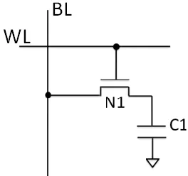
2.3 DRAM
Unlike the 6T-SRAM cell, the DRAM cell typically consists of only one transistor and one capacitor (1T-1C) as illustrated in Figure 2.3. The transistor N1 basically functions as a pass transistor with the word line (WL) connected to the gate terminal and the bit line (BL) connected to the drain terminal. In the main memory the bit line is linked to numerous DRAM cells in a column and is then the input to a sense amplifier (not shown in Figure 2.3). The word line is linked to a row of these cells and during the operation mode only one word line at a time is asserted to read or write a row. The capacitor C1 functions as a storage node. During the write operation, the word line is driven high in order to switch on the transistor. The capacitor is then charged until a desired value, which depends on the voltage on the bit line. In the read mode, the word line is first turned off and the bit line is precharged to a voltage such that it is preferably exactly in the middle between a low and a high logic level. Next, the word line is enabled and the capacitor shares its charge with the bit line. This results in a slight change in the voltage on the bit line, which the sense amplifier is able to detect and to amplify to a fully low or fully high logic level.
The drawback of the DRAM is that the capacitor for each cell is leaky, and the cell needs to be refreshed periodically to avoid loss of the stored data. Therefore, it is a dynamic and volatile memory device. The JEDEC standard requires all rows in the DRAM to be refreshed at least every 64 ms. This periodic refresh results in significant power consumption. The write speed is also slower than in SRAMs and is typically on the order of tens of nanoseconds. In addition, scaling of the DRAM is difficult mainly because of the large capacitor with a capacitance of typically 20 – 25 fF. Reducing the size of the capacitor results in less stored charge and therefore a smaller change in voltage on the bit line that the sense amplifier is to detect. This could lead to bit errors. Furthermore, the transistor cannot scale with CMOS because its leakage current needs to be very low in order to achieve a minimal refresh period of 64 ms. Regardless of this, the DRAM is widely in use in the main memory of computers. The reasons for this are that they are cost efficient and they are manufactured with a very high density, which enables overall high speed data access. DRAM chips with a size in the gigabyte (GB) scale are already common for home computers and laptops.
2.4 Nonvolatile Memory
typically used as the secondary memory storage or long term persistent storage where a slow speed may be tolerated. Nowadays, Flash memory is integrated e.g. in music players, smart cellular phones, digital cameras, digital assistants, hybrid and solid-state drives and other portable electronic consumer equipments. There are other nonvolatile memories technologies such as the FeRAM, MRAM, PCM or RRAM. However, the Flash memory is the only one that is manufactured in a high volume to date.
Flash memory is the pre-dominant nonvolatile memory technology with the fastest growing rate due in part to its compatibility with CMOS process [2.13] and its extensive development. It was invented in 1984 by Fujio Masuoka at Toshiba and Intel quickly recognized its great potential and was the first company that shipped a Flash memory chip in 1988 with an array size of 256 KB; today the capacity reaches 32 GB and higher. The Flash memory is based on the floating gate device that has a structure where a gate is embedded in the oxide of a transistor in order to store charge, and thus data. The device employs typically a continuous floating gate but in the past years a discontinuous floating gate device has been introduced where isolated nanocrystals are inserted in the oxide. This so-called nanocrystal floating gate (NCFG) device is in many aspects superior to its counterpart. Most novel NCFG devices are further modified using a high-k dielectric or a dual-layer structure to improve charge transfer and/or retention characteristics.
2.4.1 Continuous Floating Gate Device
this device. The upper electrode is the control gate, and the lower electrode is the conductive floating gate. The lower oxide that isolates the floating gate from the p-type silicon (Si) substrate is called the tunnel oxide. The upper oxide, which is inserted between the floating gate and the control gate, is called the control gate oxide, or sometimes the blocking oxide. The floating gate acts as the storage node in this nonvolatile memory device and is configured by applying the appropriate bias on the control gate, drain and source for an appropriate duration.
Figure 2.4: Schematic cross-section of a continuous floating gate device.
floating gate, a high negative voltage needs to be applied on the control gate such that the electrons tunnel back to the substrate. Then, the threshold voltage of the device shifts back towards the initial value VT0, thus erasing the device. Furthermore, VT may also become negative as shown in Figure 2.5 if the applied erasing voltage is too high and/or too long, enabling a positively charged floating gate. The amount of charge that is transferred between the floating gate and the substrate depends on several factors such as the control gate voltage, programming/erasing time, as well as tunnel and control gate oxide thicknesses. The materials that are chosen for the control gate and floating gate, as well as the oxides, also contribute significantly to the charge transfer.
Figure 2.5: Threshold voltage of an uncharged, programmed and erased device.
gate device due to its relatively thick tunnel oxide. However, as will be seen in the following Section 2.4.2, it contributes significantly to the charge transfer in a NCFG device, which uses an ultra-thin tunnel oxide. FNT is a uniform wave-mechanical tunneling process through a triangular oxide barrier and during the program mode it is applied for positive control gate voltages. It increases exponentially with an increase of the voltage or a decrease of the tunnel oxide thickness. In addition, it is strongly dependent on the barrier height in the band diagram. In the case of programming the device through CHEI, a relatively high positive voltage is also applied on the drain, which results in a large lateral electric field, especially at the drain side of the channel. This field is sufficiently high to heat up the electrons and gives rise to the impact ionization at the drain terminal. Due to the high transversal electric field between the control gate and the channel, these “hot” electrons are injected into the floating gate. Thus, this charge transfer mechanism is also known as drain side tunneling.
Figure 2.6: Mechanisms of the charge transfer in a floating gate device during (a) the program mode and (b) the erase mode. Note that the band bending in the polysilicon floating
In the erase mode FNT becomes the only significant mechanism for discharging the floating gate. Then, those electrons stored in the floating gate tunnel back to the substrate through the triangular barrier seen at the interface between the floating gate and the tunnel oxide. As indicated in Figure 2.6(b), CHEI does not apply for erasing the device due to the absence of a lateral electric field across the floating gate. Similar to the program mode, DT is only marginal compared to FNT due to the thick oxide.
It should also be noted, that programming or erasing the floating gate is not limited to charge transfer of electrons. FNT and DT of holes, as well as channel hot hole injection (CHHI) may also occur and are indicated in Figure 2.6(a) and (b) as well. However, their contribution to the overall charge transfer is small because holes are heavier than electrons and the barrier height in the valence band is higher than in the conduction band. Furthermore, charge transfer may also take place through the control gate oxide as indicated in Figure 2.6(a) and (b). This is not desired such that the control gate oxide should be designed sufficiently thick to mitigate this problem.
This in turn implies that the program/erase voltage is required to be high to enable a high electric field across the tunnel oxide. Alternatively, the program/erase time needs to be long to overcome the reduced tunneling rate. It is clear that scaling of the continuous floating gate device is limited due to SILC and this limit will be reached at the 45 nm technology node for the NOR Flash architecture and possibly 32 nm for the NAND architecture [2.15, 2.16].
2.4.2 Nanocrystal Floating Gate Device
Sandip Tiwari presented first the idea of a discontinuous floating gate with Si nanocrystals embedded in the oxide in 1995. NCFG devices have not only drawn much attention in the nonvolatile memory market since then but have recently been proposed for other applications such as a tunable gain operational amplifier, programmable reference circuit and DRAM [2.7, 2.8]. A schematic cross-section of this device is drawn in Figure 2.7(a). The nanocrystals have a diameter of just a few nanometers and an areal density of typically 1011-1013 cm-2. The tunnel oxide is thinner than in the continuous floating gate device, resulting in a more efficient charge transfer and better scalability.
Figure 2.7(b) shows a transmission electron microscopy (TEM) image of a fabricated NCFG where the Si nanocrystals have a diameter of ~4 nm in average and a density of ~6x1012 cm-2 [2.17]. The program and erase characteristics of the NCFG are very similar to the continuous floating gate device. By applying a positive voltage on the control gate the electrons tunnel from the channel to the nanocrystals and are stored there. The stored charge leads to a positive VT of the device. In order to discharge the floating gate a negative voltage needs to be applied on the control gate such that the electrons tunnel back to the channel. The mechanisms of the charge transfer of a NCFG device are now typically uniform tunneling of electrons due to FNT and DT. DT is a quantum mechanical tunneling process through a rectangular oxide barrier and increases exponentially with a decrease of the oxide. It applies only for ultra-thin oxides with a thickness of less than ~4 nm [2.18]. It is also dependent on the barrier height and the electric field across the oxide. CHEI may also apply for a NCFG device but is not typical as it is highly localized at the drain terminal and therefore not a uniform tunneling. As such, only the outer nanocrystals that are close to the drain would be charged through CHEI but would not share the charge with the other nanocrystals if their inter-particle spacing is sufficiently thick. As in the case of a continuous floating gate device, hole tunneling may also occur in a NCFG device. But again, the tunneling rate of holes is very low compared to electrons due to the heavy mass of holes and the higher barrier in the valence band.
the tunnel oxide lead to charge leakage of the entire floating gate to the substrate for a continuous floating gate device. In this case, the device changes from a programmed state to an erased state, which results in a bit error. Since these defects are very difficult to remove the lifetime of the device is practically over. In the case of a NCFG device, defects in the tunnel oxide would result in charge leakage of only the nearby nanocrystals as illustrated in Figure 2.8(b). The other nanocrystals are not affected by this and maintain their charge. Therefore, even if part of the total charge on the discontinuous floating gate is lost due to SILC, the remaining charge may be sufficient to retain the device in a programmed state.
Figure 2.8: SILC susceptibility of (a) a continuous floating gate device and (b) a NCFG device.
floating gate with an equivalent bias on the control gate. The operational voltage is also reduced, which results in a reduced power consumption. The endurance is improved and typically over 106 write and erase cycles can be achieved. In addition, the reduction of drain to floating gate coupling, and the increased gate capacity due to the thinner tunnel oxide, reduces the device susceptibility to drain induced barrier lowering (DIBL). This improves the channel length scalability of the NCFG device.
2.4.2.1 Silicon vs. Metal Nanocrystals
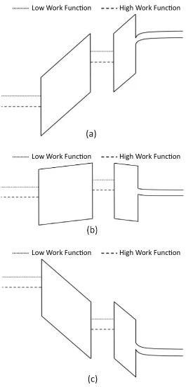
In the program mode, the use of a low or high work function metal for the nanocrystals has theoretically no influence on the tunneling rate of electrons from the channel as long as the work function is higher than the electron affinity of the channel (typically in the range of 4.0 – 4.2 eV). The conduction band in both cases is lower than in the channel such that the electrons tunnel through the same barrier. In the retention state, the electrons stored in high work function metal nanocrystals face a higher barrier to tunnel back to the channel due to the deep potential well. Therefore, the charge leakage is less than in the case of electrons that are stored in low work function metal nanocrystals. Thus, nanocrystals with a high work function metal enable further thinning of the tunnel oxide while maintaining a retention time of ~10 years, which in turns improves the scalability and charge transfer of the device. The decrease in the tunneling rate from the floating gate to the channel in the erase mode due to the higher barrier is then by part compensated by the choice of a thinner tunnel oxide.
2.4.2.2 Coulomb Blockade
The coulomb blockade effect is an important phenomenon that has been demonstrated for metal and silicon nanocrystals. As the nanocrystals in the floating gate usually vary in size the tunneling electrons select the larger sized colloids due to their lower sub-band energy and lower coulombic barrier [2.24]. Each electron that tunnels from the substrate to the nanocrystal causes a raise of the electrostatic potential in this nanocrystal by e2/2C [2.25], where e is the electron charge and C the self-capacitance of the nanocrystal. If this so-called coulomb charging energy is greater than the thermal energy, thermal noise cannot charge up the colloid any further. Therefore, the coulomb blockade effect is strongly dependent on the temperature and also the size of the nanocrystal as shown in Figure 2.10 [2.26]. A smaller size results in a smaller self-capacitance and thus a larger coulomb charging energy.
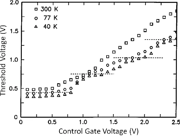
Once the larger sized nanocrystals are sufficiently charged such that their coulombic barrier is higher than in the smaller sized nanocrystals, the electrons begin to tunnel to these smaller colloids. Continuing this procedure, the entire floating gate will eventually exhibit a coulomb repulsion such that the tunneling of further electrons from the channel is blocked. These electrons can only be transferred by either raising the temperature to increase the thermal energy, or by raising the control gate voltage to increase the electric field across the tunnel oxide as illustrated in Figure 2.11 [2.24]. It can be observed, that the coulomb blockade effect is present for lower temperatures and leads to a “staircase” charging characteristics of the nanocrystals, in particular for 40 K. The tunnel and control gate oxide thicknesses are ~1.9 nm and ~9 nm, respectively. The nanocrystals have a size ranging from 2 nm to 10 nm in diameter.
2.4.2.3 Advanced Nanocrystal Floating Gate Devices
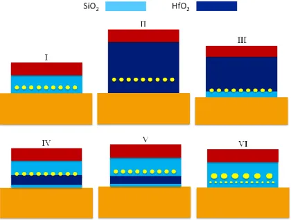
Most recently, a wide range of variations of the NCFG device have been investigated
and their schematic cross-sections are illustrated in Figure 2.12 [2.27-2.33]. The devices II-V imply the use of HfO2 as an insulator (HfAlO, HfSiO, ZrO2 or Al2O3 are also common) while the device VI consists of a dual-layer NCFG structure.
Figure 2.12: Conventional NCFG device (I) and its modified versions (II-VI).
The use of a high-k material in NCFG devices such as HfO2 offers many advantages
but also a few disadvantages towards SiO2. HfO2 is already widely integrated in modern
high dielectric constant the insulator can be physically thicker while keeping the effective
oxide thickness (EOT) similar to its counterpart. Therefore, the gate leakage current is
reduced by several orders of magnitude, which became a major problem in the last
generations of the MOSFET with SiO2 as the insulator. A comparison between these two
insulators is shown in Table 2.1.
Table 2.1: Typical properties of SiO2 and HfO2.
Parameter SiO2 HfO2
Dielectric Constant 3.9 25
Band Gap 9 eV 5.8 eV
Electron Affinity 0.9 eV 2.9 eV
Effective Electron Mass 0.4 m0 0.17 m0 Conduction Band Offset with Si 3.1 eV 1.1 eV
m0 is the free electron mass and given by ~9.109x10⁻³¹ kg. In NCFG devices the
higher dielectric constant of HfO2 enables enhanced coupling of the surrounding electrodes [2.28, 2.34]. In the case of device II in Figure 2.12, a lower programming voltage can be achieved due to the smaller conduction band offset (i.e. barrier height) at the interface
between the Si substrate and the HfO2 tunnel oxide and the charge leakage can be reduced
adhesion causes various problems such as mobility degradation, poor thermal stability or
poor interface quality whereas the interface between SiO2 and Si is very good [2.36]. In addition, an interfacial SiO2 growth between HfO2 and Si is difficult to avoid [2.37], which results in less efficient charge transfer. These fabrication issues are prevented in the devices
III, IV and V. Device III uses HfO2 as the control gate oxide to enable a stronger coupling
between the floating gate and the channel. Device IV has an additional HfO2 layer in the
tunnel oxide between the floating gate and the SiO2 to improve both the retention time and
charge transfer compared to a SiO2-only tunnel oxide. In device V the tunnel oxide is
composed of a symmetric SiO2/HfO2/SiO2 stack to obtain similar benefits as device IV with
the additional feature of equal (or almost equal) program and erase characteristics. In these
cases, the charge transfer is reduced due to the SiO2 layer in the tunnel oxide compared to the
HfO2-only device II but still superior to the conventional SiO2-only NCFG device I.
Device VI uses SiO2 for both the tunnel and control gate oxide but it has a dual-layer
NCFG structure with the ability to improve both retention time and memory window [2.32, 2.35]. The bottom layer is comprised of very small nanocrystals that are energetically unfavorable for charge storage. Most likely, the electrons will step through them and tunnel
further to the top layer during the program mode. Then, the small nanocrystals in the bottom
layer exploit coulomb blockade such that electron back-tunneling from the top layer is
mostly suppressed, which results in an improved retention time. Furthermore, the top layer
provides increased storage capacity in order to enlarge the memory window.
Table 2.2: Comparison of the conventional single-layer NCFG device and its variations.
Figure 2.12 [Ref] Tunnel Oxide Control Gate Oxide
NC Diameter, Density
Prog. Time,
Voltage Voltage Shift
Charge Loss, Retention [2.38] 3.5nm (SiO2) 8nm (SiO2) 3.2nm, 2e11cm
-2
(Si) 1µs, 10V 10ms, 10V
ΔVT=0.2V ΔVT=1V [2.39] 3nm (SiO2) 36nm (SiO2) 6nm, 4e11cm
-2
(Au) 5s, 3V ΔVT=0.6V [2.40] 2.8nm (SiO2) 6nm (SiO2) 6nm, 5e11cm
-2
(Si) 1µs, 8V 10ms, 8V
ΔVT=0.2V ΔVT=0.6V [2.27] 5.1nm (HfO2) 15nm (HfO2) 5e11cm
-2
(Ni) 1s, 3V ΔVT=0.8V 20%, 5e4s [2.28] 5nm (HfAlO) 8nm (HfAlO) 7-10nm,2e11cm-2 (Ge) 100ms, 7V ΔVT=1.5V
40%, 1e3s [2.29] 4.5nm (HfO2) 13nm (HfO2) 7.4nm, 1e11cm-2 (Si)
5s, 4V 100µs, 5V
ΔVT =0.4V ΔVT=0.2V
25%, 5e4s
[2.33] 4nm (SiO2) 24nm (Al2O3) 2-3nm,2.7e12cm -2
(Au) 16ms, 15V ΔVFB=2V 0.009V/s
[2.30]
1.5nm (SiO2) 2nm EOT (HfO2) 1.5nm (SiO2)
7nm (SiO2) 100µs, 6V Programmed 10 years
[2.31]
1.6nm (SiO2) 1.8nm EOT (HfO2) 1.6nm (SiO2)
7nm (SiO2) 100µs, 10V Programmed 10 years
[2.31] 1.5nm (SiO2) 4nm EOT (ZrO2)
7nm (SiO2) 100µs, 7V Programmed 10 years
[2.32]
2.4nm (SiO2) 2-3nm (SiO2) 20-30nm (SiO2)
5nm (Au) 1nm (C60)
2.4.3 Emerging Nonvolatile Memory Technologies
Next to the floating gate device, there are other nonvolatile memory devices that are under extensive research. Their goal is to obtain long retention time, high endurance, high switching speed, and low power consumption while keeping its cell size small.
2.4.3.1 FeRAM
The FeRAM is based on a metal-ferroelectric-insulator-semiconductor (MFIS) structure and stores the data in a ferroelectric film as illustrated in Figure 2.13 [2.3, 2.41]. The ferroelectric material is typically a perovskite material and can be polarized by an electric field where the dipoles align themselves in the same direction of the field. A change in direction results in a displacement of the dipoles in the crystal structure of the ferroelectric material. The distribution of the charge is then also shifted. Therefore, the material shows hysteresis characteristics, which enables two stable states of the device. However, the FeRAM has several challenges: the read operation is destructive and is expected to have an endurance similar to the write operation. In addition, the cell size is relatively large, the cost per bit is high, and the compatibility with CMOS is poor [2.42].
2.4.3.2 MRAM, SPRAM
The MRAM technology stores the data by magnetic storage elements and uses a magnetic tunnel junction (MTJ). There are two kinds of MRAM: i) the conventional MRAM where the magnetic field is generated due to the current flow in the word line and the bit line as shown in Figure 2.14(a) [2.43], and ii) the advanced spin transfer torque RAM (SPRAM) where the write operation is performed by the current flow through the MTJ itself and a write word line is not required as shown in Figure 2.14(b) [2.43]. The MTJ is composed of two ferromagnetic plates which are separated by a thin oxide layer, composed of a magneto-resistive material [2.3, 2.43]. One plate is a permanent magnet and is set to a fixed polarity; while the other plate is a free layer whose polarity can be changed. The electric resistance of the MTJ changes with the orientation of the magnetic field. Usually, if the polarities of the two plates are the same, the resistance is very low, resulting in a logic „1‟. If the polarities are opposite, the resistance is increased by orders of magnitude, which represents a logic „0‟. The data is therefore stored in a magnetic state of bit and is then read by sensing the resistance.
The MRAM offers high speed, excellent endurance, and low voltages. One issue is the high cost per bit which is related to its incompatibility with CMOS process. In addition, it shows thermal instability in its back-end process and requires a high write current. The SPRAM can operate with a reduced write current which enables better scalability [2.43]. Furthermore, a SPRAM with vertical MOSFET is proposed in [2.43] where the bit line, word line, transistor, and MTJ are stacked vertically. With this structure, the cell size may be as small as 4F2. Other key benefits can be summarized as high drivability, low power consumption, and good integration of logic-in-memory architecture.
2.4.3.3 PCM
The PCM, also known as PRAM or ovonic unified memory (OUM), is another potential candidate for the driving force in the nonvolatile memory market in the foreseeable future. A three-dimensional (3D) device structure is illustrated in Figure 2.15 [2.44].
Figure 2.15: Typical structure of the PCM [2.44].
chalcogenide material that is capable of reversible phase transitions between amorphous and crystalline by applying heat. It is placed between the top electrode (bit line) and a heating element that extends from the bottom electrode (word line). The memory cell is programmed through a relatively high current that heats up the chalcogenide material and leads to a thermally induced phase change. Reading occurs by sensing the change in resistance after a phase change with a low bias. The material changes from a low resistance to a much higher resistance depending on the state of the phase. One drawback is that the PCM requires a high programming current and it is sensitive to temperature variation, which may result in unintended phase-change. Therefore, it operates in a smaller temperature window compared to for example the Flash memory.
2.4.3.4 Comparison to Flash Memory
Table 2.3: Comparison between the Flash memory and emerging nonvolatile memory alternatives.
Attribute Flash NOR
[2.3, 2.46]
Flash NAND
[2.3]
FeRAM
[2.3, 2.41, 2.43, 2.46, 2.47]
MRAM
[2.3, 2.46, 2.48]
PCM
[2.3, 2.45, 2.46, 2.49]
Cell Size 10F2 4-5F2 15-100F2 10-30F2 8-20F2
Endurance 105-6 cycles 105-6 cycles 108-12 cycles 109-16 cycles 109-12 cycles Write Time 1 µs 200 µs/page 30-200 ns 10-30 ns 10-100 ns Erase Time 1 s/sector 2 ms /block 30-200 ns 30 ns 100-120 ns Read Time 20-60 ns 60 ns/serial 20-80 ns 10-30 ns 20-100 ns
Scalability Fair Fair Poor Poor Good
Multi-Bit Possible Possible No No Difficult
Cost/Bit Medium Low High High Medium
Maturity High High Medium Medium Medium
Process Full custom or +10 masks
Full custom or +10
masks
+ 2-3 masks back-end
process
+4-6 masks back-end
process
+ 2-3 masks back-end
process
2.4.3.5 Future Prospects
the cell acts as a high resistance. The switching mode between low and high resistance can be either unipolar or bipolar. There has been little demonstrated to date. However, a bipolar switching speed of 20 ns to set, and 60 ns to reset, with a data retention time of >105 s is reported in [2.51]. One of the greatest challenges of the RRAM is to control the formation and rupture of the filament. It is still in the beginning of development and it is a challenge to improve its reliability and retention. In addition, it suffers from a high on-resistance for CMOS integration.
Other nonvolatile memories that have not reached the maturity level yet to be integrated as the next generation nonvolatile memory, but should be mentioned, are the CNT memory, molecular memory, polymer memory and probe storage. The concepts for these memories are relatively new. A roadmap of the technology advancements from December 2007 of the emerging nonvolatile memories [2.52] is illustrated in Figure 2.16.
2.5 Summary
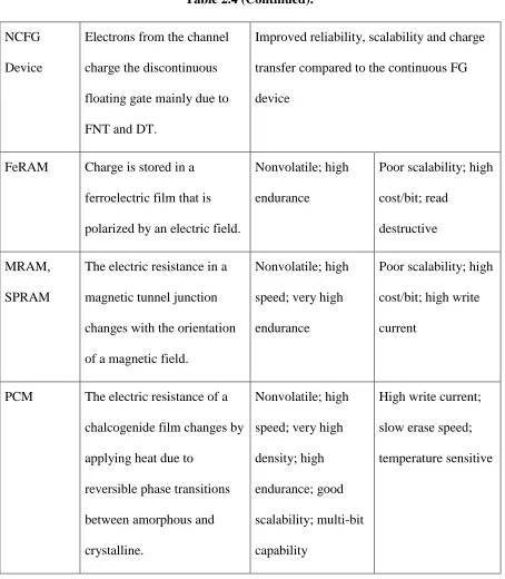
The memory is a growing field in the integrated circuit design and high efforts are being made to keep this trend by improving existing technologies and finding new solutions for the future. This Chapter provides an overview of the current volatile and nonvolatile memory technologies. Those that are well (or fairly well) established are summarized in Table 2.4.
Table 2.4: Description and key attributes of the most common memory technologies.
Technology Description Advantages Disadvantages
SRAM Charge is stored via two cross-coupled inverters.
Very high speed Volatile; large area; low density; cost and power inefficient DRAM Charge is stored on a
capacitor that shares the charge with the bit line.
High speed; high density; cost efficient
Volatile; constant refresh required; high power consumption Continuous
FG Device
Electrons from the channel charge the continuous floating gate mainly due to FNT and CHEI.
Nonvolatile; very high density; cost efficient; low idle power consumption; multi-bit capability
Table 2.4 (Continued).
NCFG Device
Electrons from the channel charge the discontinuous floating gate mainly due to FNT and DT.
Improved reliability, scalability and charge transfer compared to the continuous FG device
FeRAM Charge is stored in a ferroelectric film that is polarized by an electric field.
Nonvolatile; high endurance
Poor scalability; high cost/bit; read
destructive MRAM,
SPRAM
The electric resistance in a magnetic tunnel junction changes with the orientation of a magnetic field.
Nonvolatile; high speed; very high endurance
Poor scalability; high cost/bit; high write current
PCM The electric resistance of a chalcogenide film changes by applying heat due to
reversible phase transitions between amorphous and crystalline.
Nonvolatile; high speed; very high density; high endurance; good scalability; multi-bit capability
Table 2.4 (Continued).
RRAM A filament in an ultra-thin dielectric is formed or broken by appropriate biases on the upper and lower electrode.
Nonvolatile; high speed; ultra-high density (3D stacking); good scalability High on-resistance; good reliability and retention is a challenge; difficult control of the
formation/rupture of the filament
References
[2.1] C.-H. Wu, "A Time-Predictable System Initialization Design for Huge-Capacity Flash-Memory Storage Systems," In: Proceedings of the 6th IEEE/ACM/IFIP International Conference on Hardware/Software Codesign and System Synthesis, pp. 13-18, 2008.
[2.2] A. Padovani, "Modeling and Reliability of Innovative Flash Memories," Università degli Studi di Ferrara, Ph.D. Dissertation, 2008.
[2.3] R. Bez and A. Pirovano, "Non-Volatile Memory Technologies: Emerging Concepts and New Materials," Materials Science in Semiconductor Processing, vol. 7, pp. 349-355, 2004.
[2.4] A. Rani, "Simulation and Modeling of SONOS Non-Volatile Memory," George Mason University, Master Thesis, 2010.
[2.6] V.G. Moshnyaga, H. Vo, G. Reinman, and M. Potkonjak, "Reducing Energy of DRAM/Flash Memory System by OS-Controlled Data Refresh," IEEE International Symposium on Circuits and Systems, pp. 2108-2111, 2007.
[2.7] S. Wang, J. Dai, E.-S. Hasaneen, L. Wang, and F. Jain, "Programmable Threshold Voltage Using Quantum Dot Transistors for Low-Power Mobile Computing," IEEE International Symposium on Circuits and Systems, pp. 3350-3353, 2008.
[2.8] S.A. Rao, R.F. Steimle, M. Sadd, C.T. Swift, B. Hradsky, S. Straub, T. Merchant, M. Stoker, S.G.H. Anderson, M. Rossow, J. Yater, B. Acred, K. Harber, E.J. Prinz, B.E. White, Jr. and R. Muralidhar, "Silicon Nanocrystal Based Memory Devices for NVM and DRAM Applications," Solid-State Electronics, vol. 48, pp. 1463-1473, 2004. [2.9] A. Basu, S. Brink, C. Schlottmann, S. Ramakrishnan, C. Petre, S. Koziol, F. Baskaya,
C.M. Twigg, and P. Hasler, "A Floating-Gate-based Field-Programmable Analog Array," IEEE Journal of Solid-State Circuits, vol. 45, pp. 1781-1794, 2010.
[2.10] V. Srinivasan, G.J. Serrano, J. Gray, and P. Hasler, "A Precision CMOS Amplifier Using Floating-Gate Transistors for Offset Cancellation," IEEE Journal of Solid-State Circuits, vol. 42, pp. 280-291, 2007.
[2.11] E. Ozalevli, H.-J. Lo, and P.E. Hasler, "Binary-Weighted Digital-to-Analog Converter Design Using Floating-Gate Voltage References," IEEE Trans. on Circuits and Systems I: Regular Papers, vol. 55, pp. 990-998, 2008.
[2.12] B.P. Degnan, C.J. Duffy, and P.E. Hasler, "Crossbar Switch Matrix for Floating-Gate Programming Over Large Current Ranges," In: Proc. of 2010 IEEE Int. Symp. on Circuits and Systems, pp. 861-864, 2010.
[2.13] Y. Zhu, "Engineering the Nanocrystal Floating Gates for Nonvolatile Flash Memory Devices," University of California, Riverside, Ph.D. Dissertation, 2007.
[2.14] International Techonology Roadmap for Semiconductors (ITRS).
[2.15] Y.S. Shin, M. Div, S.E. Co, and S.K. Gyeonggi-Do, "Non-Volatile Memory Technologies for Beyond 2010," IEEE Symposium on VLSI Circuits - Digest of Technical Papers, pp. 156-159, 2005.
[2.16] G. Atwood, "Future Directions and Challenges for ETox Flash Memory Scaling,"
IEEE Transactions on Device and Materials Reliability, vol. 4, pp. 301-305, 2004. [2.17] M.L. Ostraat, J.W. De Blauwe, M.L. Green, L.D. Bell, M.L. Brongersma, J.
[2.18] K.F. Schuegraf, C.C. King, and C. Hu, "Ultra-Thin Silicon Dioxide Leakage Current and Scaling Limit," IEEE Symposium on VLSI Technology - Digest of Technical Papers, pp. 18-19, 1992.
[2.19] Z. Liu, C. Lee, V. Narayanan, G. Pei, and E.C. Kan, "Metal Nanocrystal Memories - Part I: Device Design and Fabrication," IEEE Transactions on Electron Devices, vol. 49, pp. 1606-1613, 2002.
[2.20] Z. Liu, C. Lee, V. Narayanan, G. Pei, and E.C. Kan, "Metal Nanocrystal Memories – Part II: Electrical Characteristics," IEEE Transaction on Electron Devices, vol. 49, pp. 1614-1622, 2002.
[2.21] K.S. Seol, S.J. Choi, J.-Y. Choi, E.-J. Jang, B.-K. Kim, S.-J. Park, D.-G. Cha, I.-Y. Song, J.-B. Park, Y. Park, and S.-H. Choi, "Pd-Nanocrystal-Based Nonvolatile Memory Structures with Asymmetric SiO2/HfO2 Tunnel Barrier," Applied Physics Letters, vol. 89, 2006.
[2.22] N. Miura, T. Nanjo, M. Suita, T. Oishi, Y. Abe, T. Ozeki, H. Ishikawa, T. Egawa, and T. Jimbo, "Thermal Annealing Effects on Ni/Au Based Schottky Contacts on n-GaN and AlGaN/GaN with Insertion of High Work Function Metal," Solid-State Electronics, vol. 48, pp. 689-695, 2004.
[2.23] S. Jeon, J.H. Han, J.H. Lee, S. Choi, H. Hwang, and C. Kim, "High Work-Function Metal Gate and High-k Dielectrics for Charge Trap Flash Memory Device Applications," IEEE Transactions on Electron Devices, vol. 52, pp. 2654-2659, 2005. [2.24] S. Tiwari, F. Rana, K. Chan, L. Shi, and H. Hanafi, "Single Charge and Confinement Effects in Nano-Crystal Memories," Applied Physics Letters, vol. 69, pp. 1232-1234, 1996.
[2.25] K. Yano, T. Ishii, T. Hashimoto, T. Kobayashi, F. Murai, and K. Seki, "Room-Temperature Single-Electron Memory," IEEE Transactions on Electron Devices, vol. 41, pp. 1628-1638, 1994.
[2.26] W.S. Pitts, N. Di Spigna, and P. Franzon, "Nanocrystal Film Devices and Circuits,"
SRC Review Meeting, 2008.
[2.28] J.H. Chen, Y.Q. Wang, W.J. Yoo, Y.-C. Yeo, G. Samudra, D.S. Chan, A.Y. Du, and D.-L. Kwong, "Nonvolatile Flash Memory Device Using Ge Nanocrystals Embedded in HfAlO High-k Tunneling and Control Oxides: Device Fabrication and Electrical Performance," IEEE Transactions on Electron Devices, vol. 51, pp. 1840-1848, 2004. [2.29] J.J. Lee, X. Wang, W. Bai, N. Lu, and D.-L. Kwong, "Theoretical and Experimental
Investigation of Si Nanocrystal Memory Device with HfO2 High-k Tunneling Dielectric," IEEE Transactions on Electron Devices, vol. 50, pp. 2067-2072, 2003. [2.30] J. Buckley, B. De Salvo, G. Ghibaudo, M. Gely, J.F. Damlencourt, F. Martin, G.
Nicotra, and S. Deleonibus, "Investigation of SiO2/HfO2 Gate Stacks for Application to Non-Volatile Memory Devices," Solid-State Electronics, vol. 49, pp. 1833-1840, 2005.
[2.31] B. Govoreanu, P. Blomme, M. Rosmeulen, J. Van Houdt, and K. De Meyer, "VARIOT: a Novel Multilayer Tunnel Barrier Concept for Low-Voltage Nonvolatile Memory Devices," IEEE Electron Device Letters, vol. 24, pp. 99-101, 2003.
[2.32] K. Afshari, "Nonvolatile Memory with Multi-Stack Nanocrystals as Floating Gates,"
National Nanotechnology Infrastructure Network Electronics, pp. 38-39, 2007.
[2.33] C.-C. Wang, Y.-K. Chiou, C.-H. Chang, J.-Y. Tseng, L.-J. Wu, C.-Y. Chen, and T.-B. Wu, "Memory Characteristics of Au Nanocrystals Embedded in Metal-Oxide-Semiconductor Structure by Using Atomic-Layer-Deposited Al2O3 as Control Oxide," Journal of Physics D: Applied Physics, pp. 1673-1677, 2007.
[2.34] S. Das, K. Das, R.K. Singha, A. Dhar, and S.K. Ray, "Improved Charge Injection Characteristics of Ge Nanocrystals Embedded in Hafnium Oxide for Floating Gate Devices," Applied Physics Letters, vol. 91, 2007.
[2.35] P. Dimitrakis and P. Normand, "Semiconductor Nanocrystal Floating-Gate Memory Devices," Materials Research Society Symposium Proceedings, vol. 830, 2004.
[2.36] D. Misra, H. Iwai, and H. Wong, "High-k Gate Dielectrics," Electrochemical Society Interface, 2005.
[2.37] T.-H. Hou, C. Lee, V. Narayanan, U. Ganguly, and E.C. Kan, "Design Optimization of Metal Nanocrystal Memory – Part II: Gate-Stack Engineering," IEEE Transactions on Electron Devices, vol. 53, pp. 3103-3109, 2006.
[2.39] C. Lee, U. Ganguly, V. Narayanan, T.-H. Hou, and J. Kim, "Asymmetric Electric Field Enhancement in Nanocrystal Memories," IEEE Electron Device Letters, vol. 26, pp. 879-881, 2005.
[2.40] C.M. Compagnoni, D. Ielmini, A.S. Spinelli, and A.L. Lacaita, "Modeling of Tunneling P/E for Nanocrystal Memories," IEEE Transactions on Electron Devices,
vol. 52, pp. 569-576, 2005.
[2.41] K. Takeuchi, "Ferroelectric-Gate FET for Flash Memory & SRAM (CMOS) from Design/System Perspective," ITRS ERD/ERM Memory Workshop Presentation, April 2010.
[2.42] L. Baldi, "Technology Limitations FeRAM," ITRS ERD/ERM Memory Workshop Presentation, April 2010.
[2.43] T. Endoh, "Emerging Research Memory Technologies Spin Transfer Torque MRAM (SPRAM) and its Application," ITRS ERD/ERM Memory Workshop White Paper,
April 2010.
[2.44] M.K. Qureshi, V. Srinivasan, and J.A. Rivers, "Scalable High Performance Main Memory System Using Phase-Change Memory Technology," Proc. of the 36th Int. Symp. on Computer Architecture, pp. 24-33, 2009.
[2.45] H.-S.P. Wong, S. Raoux, S.B. Kim, J. Liang, J.P. Reifenberg, B. Rajendran, M. Ashegi, and K.E. Goodson, "Phase Change Memory," ITRS ERD/ERM Memory Workshop White Paper, April 2010.
[2.46] H. Hidaka, "Embedded Flash Memory," in Embedded Memories for Nano-Scale VLSIs, K. Zhang, Ed., ed New York, NY: Springer US, 2009,pp. 177-240.
[2.47] G.R. Fox, R. Bailey, W.B. Kraus, F. Chu, S. Sun, and T. Davenport, "The Current Status of FeRAM," in Ferroelectric Random Access Memory: Fundamentals and Applications, H. Ishiwara, M. Okuyama, and Y. Arimoto, Eds., Berlin, Germany: Springer-Verlag, pp. 139-148, 2004.
[2.48] L. Tran, "STT-MRAM Challenges," ITRS ERD/ERM Memory Workshop Presentation, April 2010.
[2.49] L. Tran, "Phase Change Memory Challenges," ITRS ERD/ERM Memory Workshop Presentation, April 2010.
[2.51] N. Xu, L.F. Liu, X. Sun, C. Chen, Y. Wang, D.D. Han, X.Y. Liu, R.Q. Han, J.F. Kang, and B. Yu, "Bipolar Switching Behavior in TiN/ZnO/Pt Resistive Nonvolatile Memory with Fast Switching and Long Retention," Semiconductor Science Technology, vol. 23, 2008.
Chapter 3
A SPICE Compatible Physical Model of Nanocrystal
Floating Gate Devices for Circuit Simulation
3.1
Motivation
The majority of the single-layer NCFG research has been done at the device level. Circuit level research is still in its early stages due to the lack of a fast computing physical model for circuit simulations. To facilitate the circuit designer using NCFG devices and enable them to explore the advantages of the features of these devices as described in Chapter 2, a compact circuit simulation model is required. Several NCFG device models have been proposed in the past. Many use a numerical approach either by incorporating Monte Carlo simulations [3.1-3.3] or by solving Schrödinger-Poisson equations [3.4-3.8], which need to be solved numerically and require long computation time. Therefore, these device models are not suitable for dynamic simulations of large and complex circuits because the simulation time would be unacceptable. Alternatively, a circuit simulation model is reported in [3.9] which is easy to integrate in the existing SPICE-based infrastructure. However, it is not a physical model and therefore it cannot be used for a circuit’s power consumption computation and speed analysis.
configurable physical model of the NCFG device for circuit simulation. The main contribution is a Verilog-A module that captures the physical behaviors of programming and erasing the device. It uses only explicit formulas without any correction factors or curve fitting and can be used in any SPICE simulator supporting Verilog-A. It interacts dynamically with the rest of the circuit and includes charge leakage, which enables power consumption analysis. This Chapter is important to bridge the gap between device and circuit level research.
3.2
Introduction
This Chapter describes a comprehensive and accurate physical model of NCFG devices, which is suitable for both DC and transient circuit simulations. It is based on uniform direct tunneling and Fowler-Nordheim tunneling of electrons. The physical behavior of charging and discharging the device is implemented in a Verilog-A module to provide portability across various SPICE-based circuit simulators. It has the control gate voltage as the input state variable and computes the floating gate voltage of the device. This floating gate voltage is then connected to the gate terminal of a predictive NMOS transistor which is used for modeling conduction channel behavior in order to obtain the current-voltage (I-V) characteristics.
These parameters are listed below:
• Gate length (nm)
• Gate width (nm)
• Control gate oxide thickness (nm)
• Dielectric constant in the control gate oxide
• Tunnel oxide thickness (nm)
• Dielectric constant in the tunnel oxide
• Control gate work function (eV) • Floating gate work function (eV)
• Nanocrystal diameter (nm)
• Nanocrystal density (cm-2)
• Bulk doping (cm-3)
• Ion implanted channel doping (cm-3) • Ion implanted channel depth (nm)
• Free electron mass in silicon (kg)
• Effective electron mass in the tunnel oxide (kg)
• Effective electron mass in the control gate oxide (kg)
• Surface interface charge (C) • Temperature (K)

![Figure 2.12 [Ref]](https://thumb-us.123doks.com/thumbv2/123dok_us/1297515.1162346/42.792.74.717.107.492/figure-ref.webp)
![Figure 2.16: Status of the widely known emerging nonvolatile memories [2.52].](https://thumb-us.123doks.com/thumbv2/123dok_us/1297515.1162346/48.612.105.527.413.636/figure-status-widely-known-emerging-nonvolatile-memories.webp)