Analysis and Optimization of 1200V Silicon Carbide Bipolar Junction Transistor
228
0
0
Full text
(2) Analysis and Optimization of 1200V Silicon Carbide Bipolar Junction Transistor by Yan Gao. A dissertation submitted to the Graduate Faculty of North Carolina State University in partial fulfillment of the requirements for the Degree of Doctor of Philosophy Electrical Engineering Raleigh, North Carolina 2007 APPROVED BY:. ______________________________. ______________________________. Dr. Mesut E Baran. Dr. Mo-Yuen Chow. _____________________________. ______________________________. Dr. Doug Barlage. Dr. Alex Q. Huang Chair of Advisory Committee.
(3) BIOGRAPHY. Yan Gao, is from Shandong, China. She received her B.S. degree from Shandong University, Jinan, China. She enrolled as a Master’s student at Beijing Polytechnic University and got her M.S. in electrical engineering in July 2002. From August 2003, she began to work as a research assistant in Center for Power Electronics Systems (CPES) at Virginia Tech. In August 2004, she transferred to North Carolina State University together with her advisor Dr. Alex Q. Huang. She has been working as a research assistant in Semiconductor Power Electronics Center (SPEC) to pursue her Ph.D. degree. She was an intern at Cree Inc., Durham, NC in summer 2006. Yan Gao’s interests lie in the modeling and design of devices and circuits for power system.. ii.
(4) ACKNOWLEDGEMENTS I would like to thank my advisor, Dr. Alex Q. Huang, for his guidance, support and encouragement over the course of my graduate study and research at North Carolina State University. His knowledge, vision and creative thinking have been a source of inspiration. It was an invaluable learning experience to be one of his students. Apart from the direct input into this work, the technical discussions on various subjects provided a valuable source of ideas that will hold me in good stead for years to come. I am also grateful to my other committee members, Dr. Doug Barlage, Dr. Mo-Yuen Chow, and Dr. Mesut E Baran for their comments and suggestions. This work would not have seen the light of the day without the help of Dr. Anant Agarwal. I would like to thank Dr. Anant Agarwal at Cree Inc. for his support of this work. His expertise and advice made this work possible. I would like to thank Dr. Sumi Krishnaswami for her kind help. Her experience and organizational aptitude inspire me. I would like to thank Dr. Qingchun Zhang. His creativity and intelligence drove the indepth SiC BJT study. The countless hours of discussion has played a significant role in the completion of this work. I am indebted to all of the colleagues at Cree Inc., who made my stay at Cree during the summer internship of 2006 and subsequent visits pleasant and enjoyable. It has been a great pleasure to work with the excellent faculty, staff, and students at the Semiconductor Power Electronics Center (SPEC). The atmosphere at SPEC is highly conducive to work, due to the presence of friendly graduate students and cooperative staff.. iii.
(5) I would like to thank Mr. Jun Wang, Mr. JeeSung Juang, Mr. Yang Gao, Mr. Ding Li, Ms. Xiaojun Xu, Mr. Bin Chen, and Mr. Jinseok Park for many enlightening discussions and endless exchange of thoughts. I would also like to acknowledge Jerry Kirk for his assistance. I would like to thank my family for being the ultimate source of strength and encouragement throughout my academic career and personal life. Special thanks to my husband, Bin Fan, who has always been there with his love, understanding, and support over the years. This work was supported in part by Cree Inc., a market-leading innovator and manufacturer of semiconductors that enhance the value of LED solid-state lighting, power and communications products by significantly increasing their energy performance.. iv.
(6) TABLE OF CONTENTS LIST OF FIGURES …………………………………………………….….…………viii LIST OF TABLES……………………………...………………………….….……...xviii CHAPTER 1 INTRODUCTION ............................................................................. 1 1.1 Background .............................................................................................................................................. 4 1.1.1 Crystal Structures and Polytypes ...................................................................................................... 5 1.2 Physical and Electrical Properties ............................................................................................................ 6 1.2.1 Wide Energy Bandgap ...................................................................................................................... 7 1.2.2 High Breakdown Electric Field ........................................................................................................ 7 1.3 Improving SiC Technology ...................................................................................................................... 9 1.4 The Basic Principle of BJT Operation.................................................................................................... 12 1.4.1 Common Emitter Current Gain....................................................................................................... 14 1.4.2 Breakdown Voltage ........................................................................................................................ 16 1.4.3 Conductivity Modulation................................................................................................................ 19 1.4.4 Reverse Biased Second Breakdown Characteristics ....................................................................... 20 1.5 Outline of Dissertation ........................................................................................................................... 24. CHAPTER 2 MODELING AND OPTIMIZATION OF SIC BJT ............................ 26 2.1 Review of SiC BJTs ............................................................................................................................... 26 2.2 Electrical Models of SiC......................................................................................................................... 31 2.2.1 Mobility Model............................................................................................................................... 32 2.2.2 Incomplete Ionization ..................................................................................................................... 33 2.2.3 Recombination................................................................................................................................ 34 2.2.4 Interface States................................................................................................................................ 35 2.3 Cell Structure Optimization.................................................................................................................... 36 2.3.1 Emitter Width ................................................................................................................................. 37 2.3.2 Emitter Thickness ........................................................................................................................... 44 2.3.3 Emitter Doping ............................................................................................................................... 46 2.3.4 Base Doping.................................................................................................................................... 47 2.3.5 Spacing Between p+ Base Implant and Emitter Effect................................................................... 50 2.4 Base Resistance Model........................................................................................................................... 54 2.4.1 Metal Resistance............................................................................................................................. 55. v.
(7) 2.4.2 Cell Model ...................................................................................................................................... 57 2.4.3 Complete Base Resistance Model................................................................................................... 60 2.4.4 Base Resistance Model for Large Area BJTs ................................................................................. 63. CHAPTER 3 SIC BJT FABRICATION TECHNIQUES AND DEVICE CHARACTERIZATION ....................................................................................... 73 3.1 Fabrication Steps .................................................................................................................................... 73 3.2 Characterization...................................................................................................................................... 77 3.2.1 Voltage Blocking Capability .......................................................................................................... 78 3.2.2 Forward I-V Characteristics............................................................................................................ 81 3.2.3 Power Loss Evaluation ................................................................................................................... 98 3.2.4 Analysis of 1200V SiC BJT Inductive Switching ....................................................................... 107. CHAPTER 4 ANALYSIS OF THE SAFE OPERATION AREA (SOA) OF SIC BJTS ................................................................................................................. 121 4.1 Introduction ......................................................................................................................................... 121 4.2 RBSOA (Reverse Biased Safe Operation Area).................................................................................. 121 4.2.1 Theory.......................................................................................................................................... 122 4.2.2 Experimental Results ................................................................................................................... 125 4.3 Short-Circuit Performance of a SiC BJT ............................................................................................. 127 4.3.1 Thermal Limit.............................................................................................................................. 129 4.3.2 Electrical Limit ............................................................................................................................ 135 4.3.3 Experimental Results ................................................................................................................... 135. CHAPTER 5 ANALYSIS OF SIC BJT DEGRADATION UNDER NORMAL AND STRESSED OPERATING CONDITIONS ......................................................... 142 5.1 Introduction ......................................................................................................................................... 142 5.2 Degradation Phenomenon Type I ........................................................................................................ 143 5.3 Degradation Phenomenon Type II....................................................................................................... 146 5.3.1 Type II Degradation Summary .................................................................................................... 163 5.4 Verification of Surface Recombination Factor on Degradation .......................................................... 164 5.4.1 Extraction of Surface Recombination Factor Extraction ............................................................. 166. CHAPTER 6 MONOLITHIC INTEGRATION OF SIC BJT WITH SIC DIODE ... 168 6.1 Device structure................................................................................................................................... 169. vi.
(8) 6.1.1 BJT+ PiN ..................................................................................................................................... 169 6.1.2 BJT+ MPS ................................................................................................................................... 170 6.2 Device Fabrication............................................................................................................................... 173 6.3 Device Characterization ...................................................................................................................... 178 6.4 Summary ............................................................................................................................................. 185. CHAPTER 7 NOVEL NEW BJT STRUCTURES............................................... 186 7.1 Thick Emitter + Thin Emitter Structure............................................................................................... 186 7.1.1 Principle....................................................................................................................................... 187 7.1.2 Structure Optimization................................................................................................................. 189 7.2 Double Epitaxial Base Structure.......................................................................................................... 194 7.2.1 Structure Optimization................................................................................................................. 197. CHAPTER 8 CONCLUSIONS AND PLAN OF FUTURE STUDY ..................... 201 8.1 Major Contributions ............................................................................................................................ 201 8.2 Future works........................................................................................................................................ 203. REFERENCES ................................................................................................. 204. vii.
(9) LIST OF FIGURES Figure 1.1 The basic structural unit in SiC [19].................................................................. 5 Figure 1.2 Crystal structure of different SiC polytypes displayed parallel to the (11-2 0) plane: a) Zinkblende structure (cubic 3C-SiC), b) hexagonal 4H-SiC and c) hexagonal 6H-SiC. [19]........................................................................................................................ 6 Figure 1.3 Ron-sp comparison between SiC and Si ........................................................... 9 Figure 1.4 Internal current components in a NPN bipolar transistor................................ 13 Figure 1.5 Current components in a NPN bipolar transistor for gain calculation ............ 14 Figure 1.6 Carrier distribution profiles in the base and collector regions of a BJT under conductivity modulation conditions.................................................................................. 19 Figure 1.7 Typical turn-off waveforms under inductive load of BJT.............................. 21 Figure 1.8 Turn-off trajectory under inductive load ......................................................... 21 Figure 1.9 Electric field distribution under high current density...................................... 23 Figure 1.10 Typical safe operation area of Si BJT .......................................................... 23 Figure 2.1 A schematic cross-section of (a) an epitaxial grown emitter and (b) an implanted........................................................................................................................... 27 Figure 2.2 Comparison between demonstrated SiC BJTs and SiC MOSFETs ................ 29 Figure 2.3 Surface Fermi level pinning in simulation ...................................................... 35 Figure 2.4 Trap energy distribution .................................................................................. 36 Figure 2.5 Structure and mesh grids used in the simulation ............................................ 37 Figure 2.6 Half cell structure for emitter size effect study ............................................... 39. viii.
(10) Figure 2.7 JC/ β as a function of PE/AE ............................................................................. 40 Figure 2.8 Current gain as a function of JC at different emitter width.............................. 40 Figure 2.9 Measured current gain as a function of collector current density with different emitter width ..................................................................................................................... 41 Figure 2.10 Current gain as a function of emitter width................................................... 42 Figure 2.11 Emitter Size Effects for Jc=12, 100 and 200A/cm2 (The slope in the graph is the normalized periphery recombination base current) .................................................... 43 Figure 2.12 Normalized periphery surface recombination current as a function of collector current density.................................................................................................... 44 Figure 2.13 Beta as a function of Jc with different emitter depth .................................... 46 Figure 2.14 Beta as a function of emitter doping.............................................................. 47 Figure 2.15 Graded base doping profile ........................................................................... 48 Figure 2.16 Build-in field in the graded base ................................................................... 49 Figure 2.17 Beta as a function of current density with different base doping profile ...... 50 Figure 2.18 Beta as a function of current density with different spacing between p+ implant and emitter edge................................................................................................... 51 Figure 2.19 Lateral electron distribution in the base ........................................................ 52 Figure 2.20 Maximum current gain as a function of space between p+ implant and emitter edge ................................................................................................................................... 53 Figure 2.21 BJT layout used for base resistance study..................................................... 55 Figure 2.22 Schematic diagram of the active region in the BJT....................................... 57 Figure 2.23 2-D simulation of BE junction of a 88µm cell .............................................. 58. ix.
(11) Figure 2.24 Saber model for BE junction ......................................................................... 59 Figure 2.25 Base current flowing distribution .................................................................. 59 Figure 2.26 Saber model for base finger........................................................................... 60 Figure 2.27 Complete circuit in saber simulation............................................................. 61 Figure 2.28 Current distribution among cells ................................................................... 62 Figure 2.29 Type-I BJT layout.......................................................................................... 63 Figure 2.30 Current distribution for layout type-I ............................................................ 64 Figure 2.31 Maximum and minimum current density cells location in layout type-I ...... 65 Figure 2.32 Layout type-II................................................................................................ 66 Figure 2.33 Current distribution in type-II layout ............................................................ 67 Figure 2.34 Maximum and minimum current density cells location in the layout type-II 68 Figure 2.35 Layout type-III............................................................................................... 69 Figure 2.36 Current distribution of layout type-III........................................................... 70 Figure 2.37 Maximum and minimum current density cells location in type-III layout.... 71 Figure 2.38 Three layouts comparison.............................................................................. 72 Figure 3.1 SiC BJT ........................................................................................................... 73 Figure 3.2 Process flow for the SiC BJT .......................................................................... 75 Figure 3.3 Chip layout ...................................................................................................... 76 Figure 3.4 BJT layout ....................................................................................................... 77 Figure 3.5 Chip top view the 4H-SiC BJT under study and Packaged sample SiC BJT. 78 Figure 3.6 BVCEO and BVCBO of SiC BJT ........................................................................ 79 Figure 3.7 Gummel plot for SiC BJT ............................................................................... 79. x.
(12) Figure 3.8 BVCEO, BVCBO, BVCES at different current level............................................. 80 Figure 3.9 I-V characteristics by curve tracer................................................................... 81 Figure 3.10 Forward I-V curve measurement and simulation .......................................... 82 Figure 3.11 Hole density distribution at different base currents in the BJT ..................... 83 Figure 3.12 Carriers distribution at IC=1.26A, VCE=0.349V ............................................ 83 Figure 3.13 Potential distribution across the BJT at IC=1.26A, VCE=0.349V .................. 85 Figure 3.14 Horizontal current density distribution.......................................................... 85 Figure 3.15 BJT with conductivity modulation ................................................................ 88 Figure 3.16 Experiment setup for measurement of β as a function of collector current density ............................................................................................................................... 89 Figure 3.17 Measured and simulated current gain vs the collector current density at 300K ........................................................................................................................................... 90 Figure 3.18.Current gain vs collector current density....................................................... 91 Figure 3.19 Single pulse test I-V curves at high current of 0.0225 cm2 SiC BJT ............ 92 Figure 3.20 Beta vs Jc Extracted from Pulse IV Curves................................................... 93 Figure 3.21 SiC BJT VCEOFFSET ........................................................................................ 94 Figure 3.22 SiC BJT BE, BC junctions forward I_V curves ............................................ 94 Figure 3.23 Simulated BE and BC diode forward characteristics by a simple PN diode. 96 Figure 3.24 Calculated I-V curves for Si and SiC diode .................................................. 97 Figure 3.25 Measured I-V characteristic of Si BJT .......................................................... 98 Figure 3.26 Si BJT BE, BC junctions forward I_V curves............................................... 98 Figure 3.27 Output characteristics comparison between SiC BJT and Si IGBT ............ 100. xi.
(13) Figure 3.28 Circuit and schematic of the switching test................................................ 101 Figure 3.29 Detailed SiC BJT switching waveforms...................................................... 102 Figure 3.30 Turn off loss vs turn off current .................................................................. 102 Figure 3.31 Turn off time vs turn off current.................................................................. 103 Figure 3.32 Turn on and Turn off losses vs operating current density for SiC BJT....... 104 Figure 3.33 Comparison of switching loss vs JC between SiC BJT and Si IGBT. ......... 105 Figure 3.34 Trade-off between on-state voltage and turn off losses at the current density of 100A/cm2 .................................................................................................................... 105 Figure 3.35 Loss comparison of IGBT and 4H-SiC BJT................................................ 107 Figure 3.36 SiC BJT equivalent circuit used for switching analysis .............................. 108 Figure 3.37 Cbe as a function of Vbe ................................................................................ 109 Figure 3.38 IC rising during turn on ................................................................................ 110 Figure 3.39 IC rising during turn-on with different load current values ......................... 111 Figure 3.40 Voltage falling during turn on ..................................................................... 113 Figure 3.41 Voltage falling during turn on with different collector current................... 114 Figure 3.42 Collector current path during turn off ......................................................... 115 Figure 3.43 Voltage rising during turn off...................................................................... 116 Figure 3.44 Voltage rising during turn off with different collector current.................... 117 Figure 3.45 Equivalent circuit for discharging the capacitance Cbe ............................... 118 Figure 3.46 Current falling during turn off..................................................................... 119 Figure 3.47 IC falling during turn off with different collector current............................ 119. xii.
(14) Figure 4.1 Si and SiC breakdown voltage vs collector current when avalanche injection occurs. ............................................................................................................................. 123 Figure 4.2 Turn off failure waveform because of false turn on at VCE=1600V, IC=9A . 124 Figure 4.3 Electron current density distribution after turn-off failure at VCE=1600V, IC=9A .............................................................................................................................. 125 Figure 4.4 Single pulse measurement successful turn-off waveforms (VCE=1100v, IC=67A) ........................................................................................................................... 126 Figure 4.5 SiC and Si BJT RBSOA comparison (ST2310FX was used for comparison) ......................................................................................................................................... 127 Figure 4.6 Device cell structure used in short-circuit simulation ................................... 129 Figure 4.7 Transient simulation of different current density (solid lines) and maximum temperature (dashed lines) in the device (nonisothermal simulation). Vce=600V, Tcase=300K. ..................................................................................................................... 130 Figure 4.8 Current density distribution at different time points. (A cut along x=4.9µm) ......................................................................................................................................... 131 Figure 4.9 Transient simulation of different current density (solid lines) and energy density (dashed lines) in the device (non-isothermal simulation). Vce=600V, Tcase=300K. ......................................................................................................................................... 132 Figure 4.10 Simulated short-circuit failure..................................................................... 133 Figure 4.11 Base emitter junction forward IV at different temperatures........................ 134 Figure 4.12 Experimentally obtained on-state resistance and turn-on loss as a function of base current. Main power supply = 600V, and case temperature = 300 K.................... 136. xiii.
(15) Figure 4.13 Short-circuit test circuit ............................................................................... 136 Figure 4.14 Experimentally obtained short-circuit waveforms of non-destruction under a standard condition. Main power supply = 600 V, IB =400mA, and case temperature = 300 K............................................................................................................................... 138 Figure 4.15 Experimentally obtained short-circuit waveforms of destruction under a standard condition. Main power supply = 600 V, IB =400mA, and case temperature = 300 K............................................................................................................................... 138 Figure 4.16 BE and BC junction characteristics after short-circuit failure..................... 140 Figure 5.1 Four traces of the output characteristics of a SiC BJT with increasing cumulative stress at 10A for 0min, 15min, 30min and 16hrs.[65] ................................. 143 Figure 5.2 Degradation phenomenon type I ................................................................... 144 Figure 5.3 Degradation phenomenon type II .................................................................. 144 Figure 5.4 EBIC images of degraded device with high stacking fault activity. ............. 145 Figure 5.5 Schematic of FATBJTs ................................................................................. 147 Figure 5.6 Degradation experimental results by BE, BC junctions................................ 148 Figure 5.7 Time effect on BC junction stress ................................................................. 149 Figure 5.8 Time effect on BE junction stress ................................................................. 150 Figure 5.9 Beta as a function of time under the same base current ................................ 150 Figure 5.10 Stress current density effect on degradation................................................ 151 Figure 5.11 ∆β as a function of stress base current. ....................................................... 152 Figure 5.12 Current gain as a function of BE spacing under the same base current ...... 153 Figure 5.13 ∆β as a function of BE spacing ................................................................... 154. xiv.
(16) Figure 5.14 Gummel plot and family I-V before and after BE junction stress for 5A, 4kV BJT.................................................................................................................................. 156 Figure 5.15 Similarity between degradation effect and the emitter size effect. ............. 158 Figure 5.16 Degradation results for BJTs with different emitter width (after stress, 6µm WE BJT has a larger Ron increase and larger slope in the active region) ........................ 159 Figure 5.17 BE, BC junction I_V before and after pulse stress...................................... 160 Figure 5.18 I_V Characteristics of BJT before and after pulse stress ............................ 161 Figure 5.19 Stress results under room temperature (a) and 200ºC (b)............................ 162 Figure 5.20 Gummel plot of SiC BJT at different temperatures..................................... 163 Figure 5.21 Output Characteristics of SiC BJT before and after Stress ......................... 165 Figure 5.22 Normalized periphery surface recombination current as a function of collector current density JC for conventional structure ................................................... 166 Figure 6.1 Schematic configuration of bridge converter ................................................ 168 Figure 6.2 Cross-section schematic along BJT and PiN diode boundary....................... 170 Figure 6.3 Cross-section schematic of MPS structure diode with SiC BJT ................... 171 Figure 6.4 Cell structure used for MPS design ............................................................... 172 Figure 6.5 Doping profile of p+ belt in MPS.................................................................. 172 Figure 6.6 Trade-off curves with different schottky window opening ........................... 173 Figure 6.7 BJT integrated with different diode layout.................................................... 176 Figure 6.8 Layout detail of SiC BJT/PiN diode.............................................................. 177 Figure 6.9 Layout detail of SiC BJT/MPS diode............................................................ 177 Figure 6.10 I-V characteristics of the fabricated integrated diode................................. 178. xv.
(17) Figure 6.11 BJT/PiN Diode (a) BJT/MPS diode (b) family curves at room temperature and 200ºC........................................................................................................................ 179 Figure 6.12 I-V characteristics of the Control BJT and the BJT/diode .......................... 180 Figure 6.13 BVceo of control BJT and BJT with different design of diode................... 181 Figure 6.14 Cell structure used for SiC BJT/Diode breakdown study ........................... 181 Figure 6.15 Blocking capability of BJT/Diode in simulation......................................... 182 Figure 6.16 Leakage current flow lines when breakdown happens in simulation.......... 182 Figure 6.17 Breakdown voltage with adjusted p belt doping and thickness................... 183 Figure 6.18 Turn off waveforms of switching BJT and reverse recovery of designed PiN diode................................................................................................................................ 184 Figure 6.19 Turn off waveforms of switching BJT and reverse recovery of designed MPS diode................................................................................................................................ 184 Figure 6.20 Experimental reverse recovery currents of different integrated diodes under the same switching conditions ........................................................................................ 185 Figure 7.1 Proposed thin+thick emitter structure ........................................................... 186 Figure 7.2 Voltage potential across the BE junction of conventional BJT and the proposed structure BJT ................................................................................................... 187 Figure 7.3 Electron and hole current distribution (Y=1.95µm cut, in the thin emitter) . 188 Figure 7.4 I-V characteristic of the proposed structure and the conventional structure . 189 Figure 7.5 Thin emitter width effect ............................................................................... 190 Figure 7.6 Thin emitter width effect on current gain and the forward voltage drop ...... 190 Figure 7.7. I-V with different thick emitter width .......................................................... 191. xvi.
(18) Figure 7.8 Current gain as a function of the thick emitter width.................................... 192 Figure 7.9 Beta as a function of thin emitter thickness................................................... 193 Figure 7.10 Equivalent circuit of the proposed structure................................................ 194 Figure 7.11 Proposed double epitaxial base structure .................................................... 195 Figure 7.12 I-V comparison between double epi-base and the conventional structure .. 196 Figure 7.13 Lateral potential distribution in the base for double epi-base and conventional structures (IB=200mA, IC=5A, y=2.2µm cut) ................................................................. 197 Figure 7.14 I-V comparison between structures with different thickness of epi-p+ layer ......................................................................................................................................... 198 Figure 7.15 Equivalent circuit of the proposed double epi-base structure ..................... 199 Figure 7.16 I-V compare of structures with different second epi-p base doping ........... 200. xvii.
(19) LIST OF TABLES. Table 1.1 Electrical property of SiC and other semiconductors ......................................... 7 Table 1.2 Comparison of the material properties of Si and SiC ....................................... 10 Table 2.1 Review of SiC BJTs.......................................................................................... 30 Table 2.2 Masetti model: coefficients............................................................................... 32 Table 2.3 A summary of the optimized SiC BJT.............................................................. 53 Table 3.1 Build-in potential and voltage offset of Si, SiC BE and BC diode................... 96 Table 5.1 ∆β as a function of stress current density ....................................................... 151 Table 5.2 ∆β as a function of BE spacing with the same base current ........................... 153 Table 6.1 Surface electric field value with different p+ space opening.......................... 173 Table 6.2 BJT with PiN diode key process steps............................................................ 174 Table 6.3 BJT with MPS diode key process steps .......................................................... 175. xviii.
(20) Chapter 1 Introduction There are significant needs for more efficient, higher voltage power semiconductor devices. Application needs range from more efficient power supplies for computers and consumer appliances to electric automobile power converters, and more efficient long distance high voltage power transmission. The constant development of power semiconductor devices has always been a major factor facilitating these applications and the development of new applications. Over the last five decades, silicon (Si) has been the dominant material used for power semiconductor devices due to well controlled material property and matured device fabrication process technology. Today, Si is still the dominating material in the field of power devices. However, it is now widely recognized that silicon power-switching devices are reaching their theoretical limits of performance, as established by fundamental material parameters like the critical field for avalanche breakdown. The power transistors for 600 V and above based on Si have either a relatively high specific on resistance or significant switching power losses, which both result in high power dissipation. In addition, the maximum allowed operating temperature of Si power devices is typically 125 °C, which cannot satisfy the demand of an increasingly dense power electronics system design, such as the traction inverter used in electric vehicle. In recent years, wider band gap semiconductors have gained remarkable attention as the need for new power device materials grows due to limited Si material properties and the increasing power densities of power electronic systems. Silicon carbide is a wide band. 1.
(21) gap semiconductor that possesses extremely high thermal, chemical, and mechanical stability. SiC has the advantage of high thermal conductivity, high breakdown electric field, and saturated carrier velocity compared to other semiconductor materials, which makes it an ideal material for power devices. The commercial availability of singlecrystal SiC wafers in the early 1990s led to a resurgence of activity in the development of SiC electronic devices. SiC power devices can now be fabricated with high quality material compared to other possible wide bandgap materials. Four-inch diameter SiC wafers were recently introduced to the market for commercial applications. Due to the development of better and better SiC materials, remarkable progress has been made in SiC power devices in recent years. Over the past decade, many of the optimistic attributes of SiC power devices have been experimentally demonstrated and confirmed. Many high power SiC devices, such as diodes, transistors and thyristors have been demonstrated and SiC Schottky diodes for 600 V and 1200 V are now commercially available [3,5]. When these devices are used in a system, the low on resistance, high temperature sustaining and fast switching abilities will allow the system to work under higher frequencies, resulting in the passive components shrinking and offering an attractive cost savings. Some of the most promising applications with high demands on power density or operating temperature are hybrid electric vehicles, motor drives and power converters. Among the SiC power devices, SiC JFET and MOSFET are unipolar devices. In order to obtain a reasonable on-state resistance, SiC Junction Field Effect Transistor (JFET) is usually designed as a normally-on device. This greatly limits the application of this. 2.
(22) device due to the complex driver design. SiCED GmBH (a spin-off from Infineon) proposed a solution of SiC JFFET in series with a Si MOSFET to make the module normally off [6,7]. But this configuration cannot work in very high temperature due to the Si limitation, thus limiting the advantage of SiC devices. MOSFET is a very popular Si power switch due to its simple gate drive interface and good static and dynamic performances. Similarly, SiC MOSFET also attracts a lot of attentions [8,9,10,11]. However, due to the immature facrication process of SiC/SiO2 structure, the SiC MOSFET performance still suffers from the low effective channel mobility, which limits the on state performance of SiC MOSFETs. The SiC MOS structure may operate reliably at temperatures up to 200 ºC which is beyond the range of Si switches, however some major gate dielectric reliability issues may keep this device from being used at the extreme temperatures required by many applications [12]. Since the forward drop of a power unipolar device increases sharply with blocking voltage, most of the high-voltage high-current applications employ bipolar devices. IGBT, as a bipolar device, is widely used in converter application. However, for an IGBT, the forward voltage drop cannot be reduced below the one diode on-state drop. Since SiC has a much larger diode turn-on voltage due to its bandgap, SiC IGBT’s conduction loss exceeds silicon IGBT for low blocking voltages [13,14,15]. For this reason, the SiCIGBT is viable option for applications that require a high breakdown voltage of 5kV and more. Other challenges faced by IGBT include the lack of highly conductive p-type substrates [14].. 3.
(23) As a bipolar device, conductivity modulation will help to reduce the forward voltage drop. Compared to other bipolar devices, like IGBT and GTO, BJT does not have the junction voltage needed to overcome in order to conduct current. Also, the process complexity is reduced greatly as compared to SiC MOSFETs, rendering the SiC Bipolar Junction Transistor (BJT) a promising high power switching device. Although considerable progress has been made in recent years [16,17,18], challenges that could potentially prevent this device from reaching its full potential still exist. For example, the low common emitter current gain is one of the major technical challenges to the application of SiC BJT. The improvement of the current gain of SiC BJTs is complex since it depends on several parameters including the thicknesses and doping levels of the base and emitter layers, the material quality, and the surface passivation. The goal of this research is to improve the performance of 4H-SiC BJT with the complete study and analysis of 4H-SiC BJT using modeling and experiments. The basic operating principle, the operating limit, and the effect of both process and layout parameters will be analyzed in detail.. 1.1Background In this section, the basic material properties and advantages of SiC are described. SiC as a wide band gap semiconductor material has a high critical field and a high thermal conductivity, making it an excellent material for high power, high temperature, and high frequency power applications.. 4.
(24) 1.1.1Crystal Structures and Polytypes. SiC consists of Si and C atoms, which are both group IV element materials. Each Si atom shares electrons with four C atoms, which means that each atom is bonded covalently to four neighbors, and vice versa. The basic structural unit is shown in Figure 1.1. The approximate bond length between Si and C atoms is 1.89 Å and the length between Si-Si or C-C atoms is 3.08 Å.. Figure 1.1 The basic structural unit in SiC [19].. 5.
(25) Figure 1.2 Crystal structure of different SiC polytypes displayed parallel to the (11-20) plane: a) Zinkblende structure (cubic 3C-SiC), b) hexagonal 4H-SiC and c) hexagonal 6H-SiC. [19].. SiC embodies a characteristic known as a polytypism which means that the material can possess more than one crystal structure. Each crystal structure is called a polytype. The different polytypes are defined by their stacking sequence. The different stacking sequences for 3C, 4H, and 6H in SiC are illustrated in Figure 1.2.. 1.2 Physical and Electrical Properties SiC has a high critical field of about 2·106 V/cm, a high thermal conductivity of 3-4 W/cm.K, and a high saturated carrier velocity of 2·107cm/s. These properties make SiC devices good candidates for high power, high temperature, and high frequency applications. The physical properties of SiC and other semiconductor materials are compared in Table 1.1.. 6.
(26) Table 1.1 Electrical property of SiC and other semiconductors Property. Si. GaAs. GaN. 6H-. 4H-. SiC. SiC. 3C-SiC. Bandgap, Eg (eV at 300K). 1.12. 1.43. 3.4. 2.4. 3.0. 3.2. Critical field, Ec(V/cm). 2.5x10⁵. 3x10⁵. 3x10⁶. 2x10⁶. 2.5x10⁶. 2.2x10⁶. Thermal conductivity, λ (W/cmK at 300K). 1.5. 0.5. 1.3. 3-4. 3-4. 3-4. Saturated electron drift velocity, Vsat (cm/s). 1x10⁷. 1x10⁷. 2.5x10⁷. 2.5x10⁷. 2x10⁷. 2x10⁷. Electron mobility, µn (cm2/V.s). 1350. 8500. 1000. 1000. 500. 950. Hole mobility, µp (cm2/V.s). 480. 400. 30. 40. 80. 120. Dielectric constant, εr. 11.9. 13.0. 9.5. 9.7. 10.0. 10.0. 1.2.1 Wide Energy Bandgap Electronic devices using SiC can operate at extremely high temperatures without suffering from intrinsic conduction effects because of the wide energy bandgap.. 1.2.2 High Breakdown Electric Field SiC can withstand a voltage gradient (or electric field) more than eight times greater than that in Si or GaAs without undergoing avalanche breakdown. This high breakdown electric field enables the fabrication of very high-voltage, high-power devices such as diodes, power transistors, power thyristors and surge suppressors, as well as high power microwave devices. Additionally, it allows the devices to be placed very close together, providing high device packing density for integrated circuits.. 7.
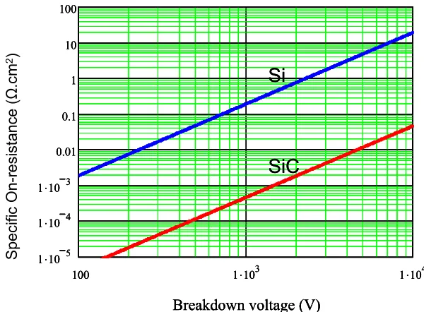
(27) From Table 1.1, SiC has a high critical field (Ec) of about 2 MV/cm. This value is about 10 times higher than that of Si. Considering the parallel-plane and abrupt N+/P junction, the relationship between critical electrical field and the breakdown voltage is given in Eqn. (1.1). ECW (1.1) 2 Where VB is breakdown voltage, EC and W are the critical field and the width of the drift VB =. region, respectively. So, to realize the same breakdown voltage, SiC device needs a much thinner drift length due to the high Ec. Assuming the current flows through the drift region uniformly without current spreading effects, the ideal specific on-resistance of the drift region is in Eqn.(1.2) Ron − sp. 4VB 2 W = = Nq μ εμ E c 3. (1.2). To realize the same breakdown voltage, an SiC device will have smaller specific onresistance due to the high Ec. The Ron-sp comparison between SiC and Si is shown in Figure 1.3. For the same breakdown voltage, the SiC device will have a Ron-sp around 1000 times lower than Si device. That means SiC device will have lower conduction loss for the same breakdown voltage design.. 8.
(28) Specific on-resitance (ohm.cm2) Specific On-resistance (Ω.cm2). 100 10. Si. 1 0.1 0.01 1 .10. 3. 1 .10. 4. 1 .10. 5. SiC. 3. 1 .10. 100. 4. 1 .10. Breakdown voltage (V) Figure 1.3 Ron-sp comparison between SiC and Si. 1.3 Improving SiC Technology SiC devices can also operate at high frequencies (RF and microwave) because of the high saturated electron drift velocity of SiC. SiC offers superior material properties to meet higher power performance challenges. Continuous power switches, power diodes, and pulsed power switches fabricated from SiC offer reductions in on-state resistance and switching loss over conventional silicon power devices. For a given power rating, these components can operate at a higher duty cycle, leading to a reduction in the size of inductors and transformers in power circuits. SiC power electronics also extend solid state technology by offering higher breakdown voltage levels than current silicon technology, addressing voltage levels now managed by electromechanical switch technology.. 9.
(29) As shown in Table 1.2, SiC devices can operate at higher temperatures and thus require less cooling. The higher blocking voltages, as compared to silicon devices, allow for the design of smaller and simpler high voltage components. Improved thermal management of semiconductors and passive components through upgraded packaging would allow more current to be handled by a given device and lead to improved power density designs.. Table 1.2 Comparison of the material properties of Si and SiC Property. Si. 4H-SiC. Benefits. Energy Band Gap (eV). 1.12. 3.26. SiC devices can operate at much higher temperatures. Electric Breakdown Field (kV/cm). 300. 2200. SiC can withstand much larger voltage gradients. 3-3.8. SiC can efficiently conduct heat away from high power junctions. Thermal Conductivity (W/cm.°C). 1.5. Power conversion equipment developed using SiC technology is projected to significantly reduce the workload and maintenance requirements for current and future carriers. As an example, use of SiC power conversion on Navy ships is expected to reduce the current conversion equipment size by approximately 60% and achieve weight savings approaching 2.68 tons for each converter implemented with the new 2.7 MVA transformer technology [1]. The major areas of the SiC device development are as follows [2]:. 10.
(30) 1.SiC wafer and substrate fabrication: The key dominating issues here lie in reducing the. physical flaws and defect densities in the wafers (such as tubular voids, referred to as micropipes and the overall residual wafer stress), and increasing wafer sizes for more cost effective fabrication. Four inch zero micropipe density SiC wafers are now commercially available [3]. 2. SiC physics and device development: This means not only the theoretical design of SiC. devices, but also the practical issues associated with layout and manufacturing processes and the building of the devices or ICs. Device engineers mainly focus on this development. 3.SiC dielectrics and Passivation: One of the key steps in making discrete devices. capable of withstanding high temperatures is proper device passivation. New materials are needed for use in device fabrication as well as final passivation coatings. 4.SiC device modeling: The ability to develop and validate accurate device models is. crucial in today’s world of computer simulations. End users should be able to simulate their circuit and system designs using device models, or they are unlikely to apply the devices themselves. Device engineers mainly focus on this development. 5. SiC packaging: Due to the high temperature operation most conventional packaging. technologies are unworkable and new technologies are needed. High temperature brazes or phase change materials are needed to allow for attachment of the SiC die. In addition, conventional power wire bonding based on aluminum must be replaced with a new technology that can withstand the high operating temperatures as well as the high currents found in many of the proposed applications.. 11.
(31) 6. SiC applications: Currently, the most promising applications for SiC are powerelectronics systems and drives, RF modules, and simple sensors. The key here is that organizations with access to SiC devices can make great strides in developing applications over those that must work completely from a theoretical perspective.. 1.4 The Basic Principle of BJT Operation The bipolar junction transistor (BJT) was invented by John Bardeen, Walter Brattain, and William Shockley at Bell Laboratories in 1947 [4]. Even though the importance of BJT has been challenged by the metal oxide semiconductor based field effect transistor (MOSFET), the BJT still has important applications that combine high power and high speed. The npn BJT is more widely used than the pnp BJT, because the electron mobility is higher than hole mobility. The bipolar power transistor is fundamentally a current-controlled three-terminal switch. It has common emitter and common base configurations. The common emitter configuration is more prevalent.. 12.
(32) Base. Emitter InE. Collector Inc. IE. IC N+. IR. IRB. N-. ICO. IPE IB. Figure 1.4 Internal current components in a NPN bipolar transistor. The basic principle of operation of the BJT is the control of the collector current by the base emitter voltage. In the forward-active mode, the base-emitter junction is forward biased and the base-collector is reverse biased. The current transport between the emitter and collector for an NPN transistor in the common base configuration is shown in Figure 1.4 with depletion boundaries and the internal current components indicated. The electrons injected from the emitter constitute the current InE. Most injected electrons, which are the minority carriers in base, will reach the collector (InC). Some electrons will recombine with majority carriers holes in base (IRB). The majority carrier holes injected from base give rise to IpE. Some electrons and holes will also recombine in the space charge region of the forward biased emitter-base junction (IR). Finally, the reversesaturation current of the base-collector junction is designated as IC0.. 13.
(33) 1.4.1 Common Emitter Current Gain. When the base-emitter junction is forward biased and the base-collector junction is reverse biased, the n-p-n BJT is biased into its active region. The current transport between the emitter and collector for an NPN transistor in the common base configuration is shown in Figure 1.5 with depletion boundaries and the internal current components indicated. The current InE is the electron current injected from emitter to the base. The current InC is the electron component at base-collector junction.. InE. Inc. IE Emitter. IC N+. N-. P. Collector. IB Base. Figure 1.5 Current components in a NPN bipolar transistor for gain calculation. Using the current components, the common emitter current gain can be written as: ΔI C ΔI nE ΔI nC ΔI C = i i (1.3) ΔI E ΔI E ΔI C ΔI nC The first term refers to as the emitter injection efficiency or gamma γ. This is a. α=. measurement of the ability of the emitter to inject electrons into the base region in an. 14.
(34) efficient manner. The second term refers to base transport factor, αT. This is a measure of the ability for electrons that injected into the base from the emitter to reach the collectorbase junction. The third term refers to the collector efficiency. This is a measure of the ability of electrons to transport through the collector region. In the case of a reverse biased collector-base junction, a strong electric field is established within a depletion region at this junction. The electrons transported through the base region are swept out by this electric filed into the collector region. At collector biases well below the avalanche breakdown voltage of the collector-base junction, this process occurs without loss of electrons. In the case of a power bipolar transistor, it is necessary to consider both the emitter injection efficiency and the base transport factor in analyzing the current gain, because unlike signal transistors the power transistors must be designed with relatively large base thickness to prevent punch-through breakdown. Now, assuming that the base emitter space charge recombination current IR can be neglected as is the case if the material quality of the base emitter junction is high, then the emitter injection efficiency γ, which is the injected electron current from the emitter divided with the total emitter current, is defined by Eqn. (1.4) ⎛ N D W ⎞ I γ = nE ≅ ⎜1 + B i E i B ⎟ I E ⎝ N E DB WE ⎠. −1. where NB, NE = base and emitter doping concentration (cm-3), DB, DE = base and emitter minority carrier diffusion coefficients (cm2/sec), WB, WE = base and emitter region widths (cm). 15. (1.4).
(35) Eqn. (1.4) holds if WE is much smaller than the hole diffusion length LpE in the emitter. If the opposite is true, then WE should be replaced by LpE. The base transport factor can be obtained:. 1 (1.5) cosh(WB / Ln ) Assuming the diffusion length is much longer than the base width (WB), the base. αT ≅. transport factor can be calculated using the following expression: WB 2 (1.6) 2 Ln 2 Two important parameters in the characterization of the bipolar transistors are the. αT ≅ 1 −. common base current gain α and common-emitter current gain β. The common-emitter current gain β is defined as the ratio of the collector and base currents as shown in Eqn (1.7).. β=. IC α = IB 1−α. (1.7). 1.4.2 Breakdown Voltage. There are two mechanisms that can limit the breakdown voltage of bipolar transistors. One phenomenon is called punch-through and it limits the open-base breakdown voltage if the total dose of the base doping is too low. As the reverse bias of the base-collector junction is increased, the base-collector depletion region can extend through the base. 16.
(36) region and reach the base-emitter depletion region. The second breakdown mechanism is the avalanche breakdown process.. (a) Open Emitter Breakdown Voltage BVCBO [20]. When BJT is operated with no connection to the emitter terminal (open emitter configuration) and a positive bias is applied to the collector terminal with respect to the base terminal, the breakdown voltage in this mode is referred to as the open emitter breakdown voltage (BVCBO). In this mode of operation, the breakdown voltage of the device is like the breakdown of a p/n- diode breakdown.. (b) Open Base Breakdown Voltage BVCEO [20]. When the BJT is operated with no connection to the base terminal (open base configuration), the breakdown voltage in this mode is referred to as the open base breakdown voltage (BVCEO). In this configuration, the leakage current flowing across the base-collector junction must flow across the emitter-base junction. Thus, the leakage current is amplified by the gain of bipolar transistor, resulting in significant enhancement in the leakage current. The leakage current for an open base transistor is shown in Eqn.(1.8). I E = IC =. 17. IL (1 − α ). (1.8).
(37) Where α is the common base current gain of the BJT, and IL is the sum of the spacecharge-generation and diffusion current across the base-collector junction. The common base current gain is given by:. α = γ E iαT i M. (1.9). Where γE is the emitter injection efficiency, αT is the base transport factor, and M is the avalanche multiplication factor. The multiplication factor (M) can be empirically related to the collector bias by: M=. 1 [1 − (VCE / BVCBO ) n ]. (1.10). From Eqn(1.8)., it can also be concluded that the collector current approaches infinity when the common base current gain approaches unity. Thus the open base breakdown voltage (BVCBO) can be obtained from the condition: M ( BVCEO ) =. 1 1 = n [1 − ( BVCEO / BVCBO ) ] α o. (1.11). Where αo is the common base current gain at low collector biases where the avalanche multiplication factor is equal to unity. From this equation, it can be shown that: BVCEO =. BVCBO ( βO ). 1. (1.12). n. Where βo is the common emitter current gain at low collector biases when the multiplication factor is unity and n is an empirical constant. Generally, n is between 3 and 6 in silicon [20]. With Si, in general, the common emitter current gain at low current. 18.
(38) levels is large, leading to an open base breakdown voltage that is substantially smaller than the open emitter breakdown voltage.. 1.4.3 Conductivity Modulation. When both the base-emitter junction and the base-collector junction are forward biased, the n-p-n BJT is biased into its saturation region. During the on-state current flow, as the current density increases, the injected carrier density also increases and ultimately exceeds the relatively low background doping of the N- drift region. When the injected hole density becomes much greater than the background doping, charge neutrality in the N- drift region requires that the concentrations of holes and electrons become equal. These concentrations can become far greater than the background doping level resulting in a large decrease in the resistance of the i-region as shown in Figure 1.6.. P. N+. N- drift. N P. n=p. noP. n. N-. p PoN+. Figure 1.6 Carrier distribution profiles in the base and collector regions of a BJT under conductivity modulation conditions.. 19.
(39) This phenomenon, called conductivity modulation, is an extremely important effect that allows transport of a high current density through the bipolar device with low on-state voltage drop. Using BJT as a bipolar transistor, the conductivity modulation in the drift region can overcome the large on-state power dissipation in unipolar devices at high blocking voltages due to increased drift layer thickness. So, for silicon, when the voltage rating is above 300V, the bipolar devices are preferred over the unipolar devices in the on-state power dissipation.. 1.4.4 Reverse Biased Second Breakdown Characteristics. The current-voltage boundary within which a power bipolar transistor can be operated without destructive failure is defined as its safe-operation-area or SOA. At low current levels this boundary is determined by the onset of avalanche breakdown(BVCEO or BVCBO). At low voltage levels this boundary is determined by the maximum current that the leads can handle without fusing. When the current and voltage are simultaneously large, the device experiences high instantaneous power dissipation. The safe operation of the device is then determined by either a thermal limitation or by an instability - referred to as second breakdown - to distinguish it from the previously discussed avalanche breakdown observed at low current levels. The second breakdown is particularly important to operation of the bipolar transistor with inductive loads. The typical turn-off waveforms of the BJT under the inductive load are shown in Figure 1.7 and the trajectory is shown in Figure 1.8.. 20.
(40) Vce. Ic. Collector Current (A). Figure 1.7 Typical turn-off waveforms under inductive load of BJT. SOA Turn off trajactory Base shorted to emitter. Collector Voltage (V). BVCEO. BVCBO. Figure 1.8 Turn-off trajectory under inductive load. The over-shoot voltage is due to the presence of a high di/dt across any stray inductance in the circuit during turn-off. During turn-off, the reverse base drive current first extracts base stored charge from the edge of emitter. As a consequence, the emitter current tends to constrict to the center of the emitter finger. In this case, the total current flowing. 21.
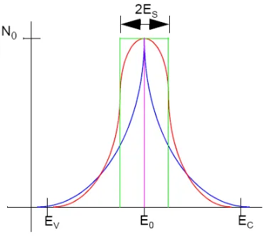
(41) through the transistor tends to remain constant while the emitter conduction area decreases. The current density at the center of the emitter then increases drastically during the turn-off process. In this case, base widening effect may occur. The peak electric field shifts from BC junction to the drift and substrate n-/n+ junction. Figure 1.9 illustrates this process, the electric field distribution shifting from 1 to 2 then to 3. The slope of distribution 3 is determined by the current density. As the current density increases, the slope increases. Once the peak electric field reaches the critical electric field, breakdown occurs. Due to the current crowding during turn-off, the extremely high current density may lead to the onset of breakdown at voltages well below the designated value. Figure 1.10 shows the typical safe operation area of Si BJT [47]. From Figure 1.10, we see the maximum operation current for this Si BJT is only 6A under the 750V bus voltage. Once the turn-off trajectory touches any point outside this area, the device turnoff will fail. The SOA is hence significantly reduced by the second breakdown. This is one of the major reasons that today’s applications uses power MOSFETs instead of BJT. MOSFETs does not have second breakdown due to its pure unipolar current conduction mechanism.. 22.
(42) Ec. Em 1. 3. Collector. Drift Nd. Base. Emitter. JIE E. Jc IC. 2. x. Figure 1.9 Electric field distribution under high current density. Figure 1.10 Typical safe operation area of Si BJT. SiC BJT has the same basic operating principle as Si BJT. However, advances in SiC material make SiC BJT overcome some of the above mentioned limitations imposed by silicon. While SiC unipolar devices are commercially available from multiple vendors [3, 5], this research investigates the current obstacles in improving and optimizing the performance of 4H-SiC bipolar junction transistors.. 23.
(43) 1.5 Outline of Dissertation Chapter 2 provides a brief review of the state-of-the-art study of SiC BJT. The main parameters are compared between different studies, and the electrical models of SiC used for the simulation study throughout the dissertation are presented. Cell structure optimization will be discussed based on those models. A base resistance model is proposed and used for the layout design. Chapter 3 provides the main fabrication steps of SiC BJT. The real fabricated SiC BJT characteristics are also discussed in this chapter. The conductivity modulation in SiC BJT is analyzed, and a thorough comparison of the SiC BJT and the popular Si power device, Si IGBT is presented in this chapter. An analytical analysis of the SiC BJT inductive switching is also presented in this chapter. In Chapter 4 the square safe operation area of the SiC BJT is demonstrated theoretically and experimentally. The SiC BJT short-circuit capability was demonstrated experimentally. Simulation study shows the theoretical limit of the short-circuit limit factor. In Chapter 5, the reliability issue - an important issue for the commercialization of SiC BJT - is discussed in this chapter. Two main types of degradation phenomena are provided, and plenty of experimental results are provided, helping to pinpoint causes of degradation. Besal plan dislocation and surface quality are cited as two main reasons for degradation.. 24.
(44) In Chapter 6 the monolithic solution of SiC BJT and diode is discussed. The proposed structure, layout, and real fabricated device characteristics are outlined. The proposed solution can help to reduce the peak reverse recovery current, system size, and cost. In Chapter 7 two types of new structures are proposed. Simulation studies regarding these structures are presented with all structures showing promising characteristics. Chapter 8 concludes the dissertation, stating the author’s contributions and providing guidelines for future work.. 25.
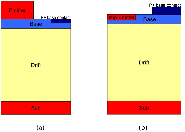
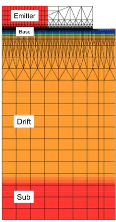
(45) Chapter 2 Modeling and optimization of SiC BJT 2.1 Review of SiC BJTs The typical cross-section view of a SiC power NPN Bipolar Junction Transistor (BJT) is shown in Figure 2.1. The mobility of electrons is also higher than holes’ hence the onresistance of NPN transistor (or the saturation voltage VCE(sat)) will be lower than the PNP BJT. Additionally, the lack of good quality of p+ substrate makes NPN BJT attracting more attention than PNP BJT. Generally, two approaches have been used to fabricate NPN SiC-BJTs. One is epitaxial growth of the emitter with a p+ implanted base contact region in the base layer (Figure 2.1 (a)). The other is an n+ implanted emitter region on a base layer after etch removal of the p+ base epitaxial growth (Figure 2.1 (b)).. 26.
(46) P+ base contact. Emitter Imp-Emitter. P+ base contact. Base. Base. Drift. Drift. Sub. Sub. (a). (b). Figure 2.1 A schematic cross-section of (a) an epitaxial grown emitter and (b) an implanted Emitter. Today, n+ epitaxial grown structures are preferred because the junction defects at the base and emitter interface generated by implantation are hard to recover completely in the annealing step. To avoid the implantation damage at the injection junction, the epitaxial emitter structure is used as shown in Figure 2.1(a). The implanted emitter SiC BJT was demonstrated by RPI group with a common emitter current gain of 8 and breakdown voltage 1KV [21]. A 1.8kV, 3.8A epitaxial emitter bipolar junction transistor was demonstrated by S-H Ryu et al. [17]. A maximum current gain of 20 was measured together with a BVCEO of 1800V for devices with an emitter pitch of 23μm. Recently, A. Agarwal et al. from Cree Inc [22] have demonstrated devices with a blocking voltage of 1600 V with current gains as high as 45 in the active region. The improved current gain was achieved by growing both the base and emitter layers in the same epi reactor and thus improving the base-emitter interface. An epitaxially grown. 27.
(47) p+ base contact region instead of implantation has been demonstrated by KTH group with a current gain only 6 [23]. The current gain reduction is presumably caused by a local reduction of the emitter efficiency by the highly doped p+ region and possibly also by a reduction of the carrier lifetime in the very high doping of NA=4×1020cm-3 [23]. Contrary to the behavior of conventional silicon devices, the current gain of these devices was found to decrease with temperature. The fact that the forward drop increases and the current gain decreases makes this device ideal for paralleling and prevents thermal runaway problems. Another interesting aspect of these devices is that the emitter size effect (ESE) was observed, meaning that current gain was found to decrease with decreasing emitter stripe width. This effect was credited to an increasing ratio of emitter periphery to emitter area of the device and the accompanying enhancement in the surface recombination of minority carriers. A review of experimentally obtained SiC BJTs results is presented in Figure 2.2 and Table 2.1. The theoretical limit for unipolar SiC power devices is also shown in Figure 2.2. Figure 2.2 clearly demonstrated that the performance of the SiC BJT is better than that of the MOSFET from the on-resistance point of view. This is due to the more uniform bulk current conduction mechanism of the BJT as compared to the surface channel and then vertical current conduction mechanism of the MOSFET.. 28.
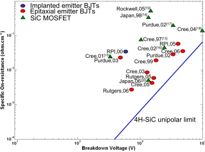
(48) Implanted emitter BJTs Epitaxial emitter BJTs SiC MOSFET. Rockwell,05[19] Japan,98[14] Purdue,02[17]. RPI,00 Cree,01[15] Purdue,03. Cree,04[18]. Cree,97[13] RPI,05 Cree,02[16] Cree,06 Purdue,02 Cree,99. Cree,03 Rutgers,05 Japan,06[20] Cree,05 Rutgers,06. 4H-SiC unipolar limit. Figure 2.2 Comparison between demonstrated SiC BJTs and SiC MOSFETs. 29.
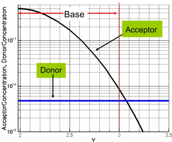
(49) Table 2.1 Review of SiC BJTs Group. Emitter (Doping[cm-3] /Thickness (µm)). Base (Doping[cm-3] /Thickness (µm)). Collector (Doping[cm-3] /Thickness (µm)). Common Emitter Current Gain (β). Ron,sp (mΩ.cm2). BVCEO (kV). Ref.. Purdue. 1e19/1. 1e17/1. 8e14/50. 15. 3.2. 41. Cree. */0.75. 2.5e17/1. 2.5e15/20. 20. 78 10.8. 1.8. 17. RPI. Implanted. 2e17/1. 4e15/12. 8. 0.5. 21. Cree. /0.75. 2e17/1. 4.4e15/15. 11. 1.3. 89. Purdue. 1e19/1. 1e17/1. 2.4e15/20. 55. 0.5. 90. Rutgers. */0.7. 3e17/0.8. 6e15/12. 32. 0.7. 91. Rutgers. 1e20/1. 8.5e17/1.4. 7e14/50. 7. 9.2. 92. RPI. 1e19/0.8. 2.3e17/1. 1e15/45. 9. 4. 93. KTH. 9e19/0.4. 1e17-1e18/0.4. 5e15/15. 6. 1. 23. KTH. 9e19/0.3. 4e18/0.3. 8e15/10. 5. -. 87. Cree. */1.5. 2e17/1. 4.8e15/15. 40. 1. 16. Rutgers. 1.3e19/0.8. 2.9e17/1. 5.5e15/15. 5. 1.6. 18. KTH. 5e19/0.6. 3e17/0.7. 4e15/15. 64. 1.1. 88. 50 8 8 17 33 56 * * 22.5 5.7 *. * not mentioned in the paper. Optimization of the current gain is quite complex since the current gain depends on the device cell structure as well as the parameters such as the material quality and the surface passivation. Optimal design is also important for device reliability. For high voltage BJT structures, the collector doping needs to be low enough to form a thick drift region of 10-15 μ m for a 1200 V SiC device. Also, the base should be designed with a sufficiently high doping dose to avoid punch-through at the maximum. 30.
(50) required blocking voltage. On the other hand, the doping concentration in the emitter usually needs to be large compared to the base doping for high emitter injection efficiency, resulting in a high current gain. However, as the emitter doping concentration increases, doping induced band-gap narrowing is effectively increased, and above some doping level the emitter injection efficiency starts to decrease. In addition, as the emitter is highly doped, the diffusion length of the minority carrier in the emitter is decreased due to increasing Auger recombination. Bandgap narrowing and Auger recombination reduce the emitter injection efficiency and thus the current gain. The high-level injection occurring in the base at high current densities also results in a reduction of the emitter injection efficiency. An accurate modeling of all relevant physical mechanisms is indispensable for identifying the impact of material properties on basic device characteristics and for device design and optimization. Furthermore, the interpretation of measurement results supported by numerical simulation is presently of particular interest in order to separate characteristics resulting from non-optimal material quality from those resulting from material properties inherent to SiC.. 2.2 Electrical Models of SiC The commercial software Integrated Systems Engineering (ISE) TCAD 10.0 [32] is used for the simulation study. In this section, the critical physical models are discussed.. 31.
Figure

+7
Related documents