Abstract
PARK, KIE JIN. The Atomic Layer Deposition of Noble Metals for
Microelectronics Applications. (Under the direction of Dr. Gregory N.
Parsons)
The purpose of this research has been to explore noble metals prepared using thermal
atomic layer deposition (ALD) for gate electrode applications in CMOS technology.
ALD Ruthenium and Rhodium metal films have been focused due to their high work
function, low resistivity of their oxidation forms. Study includes 1) ALD Ru process, 2)
ALD Ru nucleation behaviors, 3) area-selective ALD Ru process, 4) ALD Ru work
function modification, 5) ALD Rh process and work function.
For item 1), ALD Ru films were formed using ruthenocene and oxygen as precursors.
ALD window was discovered within 310 to 340°C from ALD Ru growth rate
dependence on deposition temperature. Self-limiting reaction behavior was shown from
growth rate versus precursor dose time. ALD Ru resistivity was measured to about
20~30µΩ⋅cm and Auger spectroscopy result was consistent with metallic Ru.
Foe item 2), ALD Ru was deposited on chemical SiO2, thermal SiO2, and H-terminated
Si surfaces. From thickness vs. ALD cycle, growth rates of Ru on those substrates were
similar while as initial nucleation periods were different. Contact angle values of initial
substrates showed hydrophilicity was related to the incubation time difference between
substrates. ALD Ru Nucleation behavior was investigated on H-terminated Si during
incubation period and growth model was proposed.
For item 3), extending ALD Ru nucleation study, area-selective ALD Ru process was
inhibiting nucleation. Metal-oxide-semiconductor (MOS) capacitor was fabricated using
selective deposition process and spectroscopic (XPS) and electrical
(capacitance-voltage) measurements of the capacitor confirmed the viability of selective deposition.
For item 4), ALD Ru work functions on SiO2 and HfO2 was measured and it turned out
that Ru work functions on high-k dielectrics are smaller than on SiO2 possibly due to
dipole formation at metal/dielectric interface. Organic self-assembled monolayers were
applied on high-k dielectric surfaces prior to ALD Ru deposition to modify the dipole at
the interface. ALD Ru work functions increased with amine-terminated self-assembled
monolayer and decreased with vinyl-terminated monolayer.
For item 5), ALD Rh has rarely been studied even though Rh is a candidate material for
PMOS gate electrode. We investigated and developed successful ALD Rh process using
Rhodium acetylacetonate and oxygen as precursors. ALD window was found at 280 to
310°C. It was shown that ALD Rh resistivity decreased with deposition temperature
The Atomic Layer Deposition of Noble Metals for
Microelectronics Applications
Kie Jin Park
A dissertation submitted to the Graduate Faculty of
North Carolina State University
In partial fulfillment of the
Requirements for the Degree of
Doctor of Philosophy
Chemical Engineering
Raleigh, North Carolina
2005
Approved by:
_______________________ _______________________
Dr. Jan Genzer Dr. Orlin Velev
_______________________ _______________________
Dr. Carl Osborn Dr. Gregory N. Parsons
This dissertation is dedicated to my wife, Mi Yeon Kim,
my son, John Park,
and my father, Dae Hwan Park, for all their love.
Biography
The author was born in Pusan, South Korea. He received his B.S. and M.S. degrees
in Chemical Engineering in 1991 and 1993 from Pusan National University. He worked
for Kolon Research and Development Center as a senior researcher from the January
1993 to the December 1999. He received his M.S. degree in Electrical Engineering in
Acknowledgements
I would like to express my deepest gratitude to my graduate advisor, Dr.
Gregory Parsons, for providing me both the direction and the freedom to thoroughly
experience the research process, and more importantly, for his endless guidance to help
me overcome all the technical obstacles in my thesis. I just want to let him know that he
gave me more than enough to do.
I want to thank Kit Yeung who has been a great technical teacher, a great life
teacher and a great friend.
I am also grateful to all the members, past and present, of Dr. Parsons’ research
group including Dr. Theodosia Gougousi, Dr. Atul Gupta, Dr. Kevin Bray, Dr. Dong
Niu, Jason Kelly, Leonard Nelson, David Terry, Tom Abatermarco, Powan Mehan,
Changwoong Chu, Jason Doub, Joe Spagnola, Jeong-Suk Na, Qing Peng, Katherine
Schadel and Michael Stewart.
I acknowledge Dr. Rajendra Bhatt, Dr. Micheal Tomlinson and Dr. Kirill
Efimenko in Dr. Genzer’s group for sharing their knowledge about monolayer
experiments.
I acknowledge Erik Santiso in Dr. Gubbins’ group for some very thoughtful
discussion about reaction modeling study.
I acknowledge my graduate committee members, Dr. Carlton Osburn, Dr. Jan
Genzer and Dr. Orlin Velev for their support through my graduate years and their
I am indebted to my dearest friend, Jason Kelly, discussing and advising
research and life.
I would like to thank all the cleanroom staff, especially Joan, Harold, Henry, and
Ginger. Finally, I would like to extend my deepest thanks to my wife and son, Mi Yeon
and John, for their love, understanding, and boundless support. My father and my
TABLE OF CONTENTS
LIST OF FIGURES
... viiiCHAPTER 1. INTRODUCTION
... 11.1 Background of atomic layer deposition process... 1
1.2 Advantages and limits of the ALD process... 3
1.3 Applications of ALD metals... 5
i) Back-end of line process applications... 5
ii) Gate electrode applications ... 5
1.4 Research challenges for metal gate electrodes... 7
1.5 Objective of this work... 9
1.6 Experimental Approach... 10
1.7 Overview of dissertation... 16
Reference... 19
CHAPTER 2. Microcontact Patterning of Ruthenium Gate
Electrodes by Selective Area Atomic Layer Deposition
... 312.1 Introduction... 32
2.2 Experimental... 33
2.3 Results and Discussion... 35
Reference... 38
CHAPTER 3. Atomic Layer Deposited Rhodium for PMOS Gate
Electrode Applications
... 453.2 Experimental... 47
3.3 Results and Discussion... 48
Reference... 52
4.2 Experimental... 64
4.3 Results and Discussion... 65
Reference... 69
CHAPTER 5. The Nucleation Characteristics of Ruthenium Metal
Film by Atomic Layer Deposition
... 775.1 Introduction... 78
5.2 Experimental... 79
5.3 Results and Discussion... 80
5.4 Conclusion... 81
5.5 Acknowledgements... 82
Reference... 83
LIST OF FIGURES
CHAPTER 1. INTRODUCTION
Figure 1.1 The schematic of ALD process in the simplest case……….26
Figure 1.2 (a) The energy band diagram of a N-MOS device showing the depletion
layer in the poly-Si gate. (b) The poly-Si gate depletion effect decreases the gate
capacitance in the inversion regime as evident in the capacitance-voltage plot. Taken
from reference 31……….27
Figure 1.3 The schematic of home-built hot-wall quartz tube ALD reactor…………..28
Figure 1.4 Experimental schematic of films preparation using thermal ALD
equipment………29
CHAPTER 2. Microcontact Patterning of Ruthenium Gate Electrodes
by Selective Area Atomic Layer Deposition
Figure 2.1 Ruthenium film thickness vs. number of ALD cycles as deposited on HfO2,
SiO2 and Si-H (HF-last) surfaces, compared to deposition on OTS covered substrate.
The data point at zero thickness for growth on Si-H is determined from visual
inspection. The data point at zero thickness for growth on OTS is determined from XPS.
Visual inspection shows clear selectivity on OTS for all conditions studied (up to 300
profilometer. The inset shows an optical image of a selectively deposited Ru (100µm
diameter) metal on HfO2………..41
Figure 2.2 (a) Survey scan, and (b) Ru Ru3p region from XPS analysis of a SiO2
partially covered with OTS after 150 Ru ALD cycles at 325ºC.
OTS: region with OTS covered, ALD Ru: Ru covered after on HfO2 and SiO2 compared
to deposition on OTS covered substrate……….……….42
Figure 2.3 Capacitance-Voltage behaviors of MOS capacitors………..…………43
(a) Selectively deposited ALD Ru MOS
(b) Conventionally processed MOS
Figure 2.4 VFB versus EOT for Ru/SiO2/Si and Ru/HfO2/Si Capacitors………....44
Quality of fittings (R): 0.9, the doping density of p-type Si: 1.5 x 10¹⁸/cm3, φms: the
work function difference between metal and silicon substrate
CHAPTER 3. Atomic Layer Deposited Rhodium for PMOS Gate
Electrode Applications
Figure 3.1 ALD Ruthenium film growth rate vs. deposition temperature as deposited on
CVD HfO2 substrate………...….55
Figure 3.3 XPS analysis of ALD Rh film on SiO2………..………...57
(a) Rh3d (b) O1s (c) C1 after 150 Rh ALD cycles at 300 ºC.
Figure 3.4 Resistivity of ALD Rhodium and Ruthenium films vs. deposition
temperature……….…….58
Figure 3.5 Capacitance-Voltage behaviors of selectively deposited ALD Rh MOS
capacitors………..…….…………..59
(a) on CVD HfO2
(b) on SiO2
Figure 3.6 VFB versus EOT………..…..……….60
(a) Rh/SiO2/Si and Ru/SiO2/Si
(b) Rh/HfO2/Si and Ru/HfSiOx/Si
Quality of fittings (R): 0.9, p-type silicon substrates with doping levels of 7x10¹⁷ and 3x1015 cm-3 for SiO2 and HfO2, respectively.
Figure 3.7 AFM images of ALD Rh films on (a) CVD HfO2, (b) SiO2, and (c)
H-terminated surface………...…….61
Figure 4.1 VFB versus EOT for Ru/SiO2/Si, Ru/HfO2/Si, and Ru/HfSiOx/Si
Capacitors………....72
The intercept gives Φm,eff =4.84eVon SiO2, 4.7eV HfO2, 4.68eV HfO2 surfaces
Figure 4.2 VFB vs EOT for Ru on HfSiOx films with nitric acid pretreatment steps
before metallization……….………73
The nitric acid pretreated HfSIOx shows a change in intercept consistent with a 0.2eV
decrease in effective metal work function
Figure 4.3 ATR-FTIR spectrums of monolayers on HfSiOx ……….74
(a) 3-aminopropyltriethoxysilane (APS)
(b) Undecenyltrichlorosilane (UDS)
Figure 4.4 VFB vs EOT for Ru on HfSiOx films with two different organic layer
pretreatment steps before metallization………...…………75
The APS monolayer shows a change in intercept consistent with 0.1~0.4eV increases in
effective metal work function, and the UTS monolayer shows a 0.6eV decrease in Φm,eff
Figure 4.5 VFB vs EOT after post metallization annealing for Ru on HfSiOx films with
a APS monolayer before metallization……….…...………76
Post metallization annealing: N2:H2 = 10:1, 400°C x 30min.
Figure 5.1 ALD cycle versus Ru film thickness deposited on chemical SiO2, thermal
SiO2, and H-terminated Si………...………87
Figure 5.2 Water contact angle of substrates versus nucleation incubation time…...…88
Figure 5.3 SEM and AFM images for ALD Ru deposited on chemical SiO2, thermal
SiO2, and H-terminated Si……….…..89
Figure 5.4 XPS spectrum of ALD Ru deposited on H-terminated Si surface at 0, 10, 40,
70, 100, and 150cycles………..………..90
(a) Ru3p (b) Si2p
Figure 5.5 ALD Ru thickness by XPS and profilometer vs. cycle on SiO2 and Si-H
surfaces..………..…91
Figure 5.6 AFM RMS for ALD Ru deposited on thermal SiO2 and H-terminated Si
function of ALD cycle………..…..92
Figure 5.7 SEM images as-deposited, forming gas annealed, RTA anealed ALD Ru
films………..………….……..93
Forming gas annealing: N2:H2 = 10:1, 400°C x 30 minutes
Figure 5.8 SEM and XRD analysis for ALD Ru films deposited on HfO2, HfSiOx, and
thermal SiO2………...…….94
CHAPTER 6. ALD Ruthenium Growth Model on H-terminated Si
Figure 6.1 ALD cycle versus Ru film thickness deposited on H-terminated Si…...…103
Figure 6.2 (a) XPS Ru3p of ALD Ru deposited on H-terminated Si surface at 0, 10, 40,
70, 100, and 150cycles (b) Ru3p3/2 peak values vs. ALD cycle………104
Figure 6.3 Ru thickness measured from XPS Ru3p3/2 peak and profilometer vs. ALD
cycle………...………105
Figure 6.4 XPS Si2p of ALD Ru deposited on H-terminated Si surface at 0, 10, 40, 70,
100, and 150cycles………..………...106
Figure 6.5 RMS roughness by AFM for ALD Ru deposited on H-terminated Si function
of ALD cycle……….107
Figure 6.6 Schematic of ALD Ru growth model on H-terminated Si surface……….108
Figure 6.7 Comparison of ALD Ru growth by experimental and model on H-terminated
Si surface………...…109
Appendix. Bulk and Interface Charge in Low Temperature Silicon
Nitride for Thin Film Transistors on Plastic Substrates
Figure 1. Infrared absorption spectra for PECVD SiNx films containing different
NH/SiH ratio at (a) T = 150oC and (b) T = 250oC, with (c) different temperature for
NH3/SiH4 = 10……….…………..123
Figure 2. Current density vs. electric field for SiNx deposited with different
NH/SiH ratio at (a) T = 150oC and (b) T = 250oC, with (c) different temperature…...124
Figure 3. C/Cox vs. voltage plots for nitride films deposited with different
NH/SiH ratio at (a) T = 150oC and (b) T = 250oC, with (c) different temperature. Note the change in the flatband voltage (VFB) with changing NH/SiH and deposition
temperature………125
Figure 4. Plots of flat band voltage versus the nitride thickness at (a) different NH/SiH
ratio at T = 150oC, and with (b) different temperature at NH3/SiH4 = 10. The symbols
are experimental data, and the solid and dashed lines are best fits to equation (1) in the
text……….126
Figure 5. The charge variation in the interface and bulk film for the films deposited
with (a) different NH/SiH ratio at T = 150oC, and with (b) different temperature at
CHAPTER 1. INTRODUCTION
1.1 Background of atomic layer deposition process
Atomic Layer Deposition (ALD) was first introduced as atomic layer epitaxy (ALE) in the
late 1970s by Suntola and co-workers as a method of depositing amorphous and
polycrystalline films for thin film electroluminescent (TFFL) displays1-4. III-V compound
semiconductors were investigated5,6 soon after the successful introduction of ALD. Since the mid 1990s, interest in ALD technology has increased rapidly in the silicon-based
microelectronics industry. This increase is a direct consequence of the ever-decreasing
device dimensions and the increasing aspect ratios in integrated circuits (IC). Traditional
thin film deposition techniques such as chemical vapor deposition (CVD) and physical
vapor deposition (PVD) are expected to meet major conformality problems during the next
few years, and ALD is currently considered a promising alternative candidate to them. At
the same time, film thicknesses are shrinking so thin that ALD’s major drawback, the low
deposition rate, is becoming less important7.
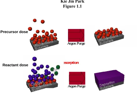
In ALD, film growth takes place in a cyclic manner. In the simplest case shown in Figure 1,
one cycle consists of four steps: i) introduction of the precursor, ii) purge or evacuation of
the reaction chamber, iii) introduction of the reactant, and iv) purge or evacuation. This
cycle is repeated as many times as necessary to obtain the desired film thickness. During
the precursor pulse, precursor molecules chemisorb, or react with surface groups, saturating
the substrate: After the formation of the chemisorbed monolayer, no further adsorption
molecules. Under these conditions, film growth is self-limiting. That is, the amount of the
film deposited during each cycle is the same and is determined only by the density of the
chemisorption or reaction sites at the surface. In an ALD process, a plot of growth rate
versus substrate temperature shows a plateau or inflection region in which self-limiting
ALD behavior exists8,9. This temperature range is often called the “ALD process window”. At temperatures below this range, excess reactant condensation typically results in a larger
growth rate, whereas insufficient activation energy for chemisorption or reaction leads to
decreased growth rate. At higher temperatures, film growth rate may be increased by
thermal decomposition of reactants or decreased by desorption of desired products or
reactants. All of these cases are deviations from the desired self-limiting ALD process.
Insufficient dosing of reactants or insufficient purging resulting in gas-phase mixing and
reaction of alternate reactants can also keep a process from being ideal self-limiting within
the ALD temperature window10. In ideal ALD, the thickness of the film would be
determined only by the self-limiting growth reaction that occurs on the surface. As long as
enough precursor gas is introduced into the reactor to saturate the surface, deposition of one
monolayer would occur each cycle. In reality even when true ALD is achieved, only a
fraction of monolayer is deposited each cycle. The non-ideality of the growth rate also
depends on several processing parameters. This behavior is sometimes due to steric
hindrance of molecular precursors adsorbing on the surface, which leads to saturation at
gas-phase species and a specific reactive site on the surface.12,13 Decreasing ALD growth rates has also been attributed to reactant desorption.14
1.2 Advantages and limits of the ALD process
Atomic Layer Deposition produces individual layers on the atomic level and allows more
choices in the type of film deposited including epitaxial, polycrystalline, and amorphous 12. In addition to this choice, film growth by the sequential deposition of monolayers (as
discussed earlier) offers ALD some characteristic advantages over more traditional CVD
and PVD techniques9,15,16. First, in ALD atomic-scale thickness control is achieved because the final film thickness depends only on the number of cycles performed. Second,
chemistries used can be highly reactive since precursor and reactant are isolated from each
other by purge or evacuation steps. This allows for a wider selection of ALD precursors
than those available for CVD and lower deposition temperatures17. Third, the ALD
characteristic of self-limiting surface reactions gives much more uniform films than CVD,
especially for films deposited on large-area wafers. This is because in each ALD step film
growth stops when the reactants saturate the surface even if reactants have higher flux in
some areas of the wafers. During CVD, non-uniformities in the reactant flux along the
wafer cause a corresponding variation in the local growth rate. For the same reason, ALD
leads to much better conformality than PVD, especially for films deposited on high
aspect-ratio structures. In other words, the film growth rate is same over all parts of 3-dimensional
structures where PVD cannot provide a conformal film due to self-shadowing. Finally,
impurities than CVD18. Because of these advantages, ALD is considered the most
promising deposition technology to replace CVD and PVD in the semiconductor industry
for applications that require high conformality and quality such as DRAM (Dynamic
Random Access Memory) trench capacitors, back-end interconnect barriers, metal gate
electrodes, and high-aspect-ration vias.15,18,19 In spite of the above advantages, ALD has some limitations keeping it from being more prevalent in production. The obvious problem
of growing a film one atomic layer at a time is the large number of cycles required to obtain
a sufficiently thick films20. In recent applications in microelectronics, however, required film thicknesses have, in many cases, decreased to the low nm range, and this has made the
low growth rates of ALD more acceptable. For example, for the 65nm interconnect
generation, the Cu diffusion barrier thickness can be no more than 5nm thick, which can be
deposited with less than 100 ALD cycles, which could typically be done in several minutes
for most cases. Another problem is the deviation from the theoretical monolayer that is
form during ALD. An imperfect, partial monolayer usually forms due to steric
limitations11,16. Other problems can disrupt the formation of the theoretical monolayer such as residual or desorbing gases20. The desorbed gas can react with the gas entering the chamber, causing unwanted by-products on or above the substrate surface. The growth of
polycrystalline films involves nucleation stages similar to those found in other deposition
methods that can cause roughening at the surface16. This is less common for epitaxially
1.3 Applications of ALD metals
i) Back-end of line process applications
With the continued scaling down of semiconductor device demension, now clearly entering
the nanoscale node, the need for a deposition technique to produce very conformal,
ultrathin films at low growth temperatures has increased. Because of its excellent thickness
control and uniformity, ALD metals are of interest especially for back-end technology
including Cu-interconnection and diffusion-barrier materials since the deposition of films in
back-end technology requires high conformality due to the very high-aspect-ratio structures.
For the sub-100nm node, copper has become the primary metal for back-end
interconnection metallization because of its low resistivity (1.67µΩ·cm) and resistance to
electromigration21. However, Cu easily diffuses through the dielectric. Thus, practical applications of Cu metallization require the presence of films that function as diffusion
barriers or adhesion/seed layers which are necessary to promote adhesion and prevent
diffusion and reaction of the Cu layer with dielectric materials. Metallic tantalum and
titanium have been deposited by ALD using metal chlorides and atomic hydrogen produced
in remote plasma,22,23 and conducting nitrides and related alloys of Ta and Ti are being studied as potential diffusion barriers. Ta-based barrier layers deposited by ALD include
TaN deposited24-26. Ti-based barrier layers deposited by ALD include TiN27-29.
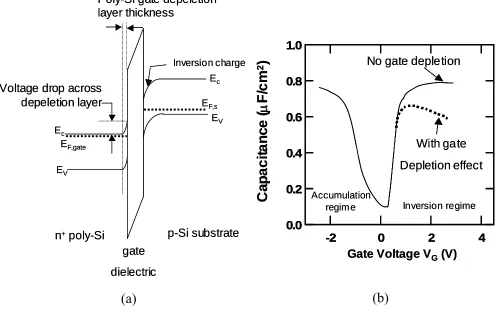
ii) Gate electrode applications
Other important applications for metals deposited by ALD include new gate metals for
devices are conventionally made of highly doped polycrystalline silicon (poly-Si). Several
issues of poly-Si have been recently encountered due to aggressive scaling. One of them is
depletion of the poly-Si gate electrode31 when the gate stack is biased in inversion, which results in reduced inversion layer charge density. This poly-depletion effect lowers gate
capacitance and typically results in an increase of 4-5 Å in the Equivalent Oxide Thickness
(EOT) of the gate stack. This effect represents a significant problem as industry targets
EOTs of less than 10 Å for sub-65nm CMOS. Other drawbacks to using poly-Si gates arise
with further scaling including boron penetration through the dielectric and poly-Si reaction
with high-k materials making it less favorable material for the continued use as a gate
electrode32,33. Metals for gate materials have several advantages over poly-Si including metals have lower resistivity than poly-Si34,35, no doping is necessary due to excess of electrons in the metal, so no boron penetration will occur, and gate depletion problem is not
as significant as poly-Si. From the point view of materials, the work function is an
important property for candidate replacement gate electrode materials with work functions
near the conduction band edge of Si (4.05eV) and near the valence band edge of Si
(5.17eV) for NMOS and PMOS devices, respectively. A single metal gate material with a
mid-gap work function for both PMOS and NMOS has been studied and turned out to not
be viable due to high threshold voltages34. To avoid high threshold voltage, a “dual-metal gate” design in which different metals are used for the PMOS and NMOS devices is a
promising solution. Besides the proper work function, prospective metals need to possess
several properties including high thermal stability, low resistivity, good adhesion to
inert elements such as Au and Pt, suffer poor etching and adhesion issues. Low-work
function (NMOS-compatible) metals such as Al and Ti often react with the dielectric and
form detrimental interface states36]. From a processing perspective, the choice of deposition technique for the gate metal is also critical as a metal deposition process that does not
damage the dielectric layer is desirable. Low impurity concentration is also required
because any impurity causes capacitance-equivalent thickness increase and prevents
long-term stability. ALD is a promising deposition technique to deal with these constraints18.
1.4 Research challenges for metal gate electrodes
Several candidate materials exist for dual metal gates (PMOS and NMOS-compatible).
Promising candidates for PMOS include Ru, and Mo for several reasons37,38. A conductive oxide such as RuO2 has also been considered a candidate for PMOS39-52 but conductive
metal oxides are not of general interest because they could potentially act as a source of
oxygen for unwanted silicon oxidation. NMOS metal gate candidates include Ti38 and Ta
(generally in nitrided compounds such as TaSixNy)53,54. Metallic Hf and Zr for NMOS
applications appear to be impractical due to high reactivities with dielectric oxides55. For a dual metal gate application, processing issues such as extra lithographic steps may also be
important obstacles to overcome. One promising approach from a process integration point
of view is the idea of depositing one metal over the entire CMOS structure then chemically
modifying the metal in one region (either NMOS or PMOS) to change its effective work
function (yielding two metallic species with both NMOS and PMOS compatibility). This
(poly-Si) is doped differently in different regions to give the appropriate work functions. It has
been shown, for example, that Molybdenum can be changed from a high-work function
metal (PMOS) to a low-work function (NMOS) metal with nitrogen implantation37. Interdiffusion is another promising technique for adjusting gate work function. Structures
in which Ti (NMOS) covers the entire structure and Ni is deposited on top of the Ti only in
the PMOS region have been deposited. Upon annealing, the Ni and Ti interdiffuse to form
an alloy that is Ni-rich at the dielectric interface and has a PMOS-compatible work function
56,57. Metal alloys have also been studied using Ru-Ta alloys, and the metal work function
tuning has been achieved by varying the alloy composition58. Nanolaminate films by ALD could be a convenient method for controlling the composition and work function of gate
metal alloys as well as integrating the deposition processes for both gate dielectric and gate
metal films22,23,59,60.
Film uniformity and growth rate during ALD greatly depend on the density and nature of
surface adsorption sites. Typically, ALD has an initial nucleation period, which is different
from cyclic steady state behavior. It is sometimes necessary to modify initial surface
properties to shorten the nucleation period. For instance, when depositing high-k dielectrics
on silicon using ALD process, surface hydroxyl groups often provide the active sites for
precursor adsorption during the initial nucleation period. Since native SiO2 is an
undesirable low-k interfacial layer for high-k dielectric applications, the native SiO2 layers
are typically etched in a dilute HF solution resulting in a surface (called HF-last) not easily
oxidized in air even up to few hours. However, ALD growth generally initiates poorly on
ALD monolayer.61 This initiation period can be shortened by re-oxidizing the HF-last Si surfaces either thermally or chemically.62. Another approach might be to nitride the HF-last Si. This approach could passivate the surface against oxidation while still allowing
precursor adsorption through the dative bonding mechanism. Similarly, surface
pretreatment techniques could be applied to passivate the top surface of high-k against
unwanted reactions with ALD metal films grown in our research.
As described in the plan of work section, our research will examine several surface
pretreatments mentioned the above. In addition, high-k layer surface terminations with
organic monolayers such as alkyls, amines, and alcohols will be examined. Research will
include blocking the deposition of ALD metals, patterning the metals, and eventually
developing a novel “selective ALD” processes. The work function is a key electrical
property for gate electrodes, but the work function of ALD deposited metals is just
beginning to be studied. The research plan described here for ALD metals focuses on the
effects of various surface terminations and substrate pretreatments on the work function
values of ALD films. Other challenges and unresolved issues including nucleation and
coalescence of ALD films, the extent of surface coverage achieved in an ALD pulse,
sufficient dosing of reactants to the substrate, and adequate purging of excess reactants
from the system will be also addressed.
1.5 Objective of this work
Our primary objective is to investigate the interface engineering of high-k dielectrics and
nucleation of ALD metals to understand surface reaction thermodynamics and kinetics. The
first goal, therefore, was to develop a thermal ALD process for metal Ruthenium. The
second goal was to investigate the nucleation behaviors as well as area-selective process of
ALD Ru on dielectric surface. The third goal was to study the electrical properties of ALD
Ru and extraction of effective work functions on SiO2 and high-k dielectrics. The fourth
goal was to understand the effect of interface dipole at metal/dielectric on metal work
function and control metal work function modifying interface from dielectric surface
treatments prior to metal deposition organic self-assemble monolayers. The fifth goal was
to investigate Rhodium ALD process as alternative gate material. Areas of interest include
studying the electrical, material properties, and effective work function of ALD Rh. They
also include interface properties and thermal stability of ALD Rh.
1.6 Experimental Approach
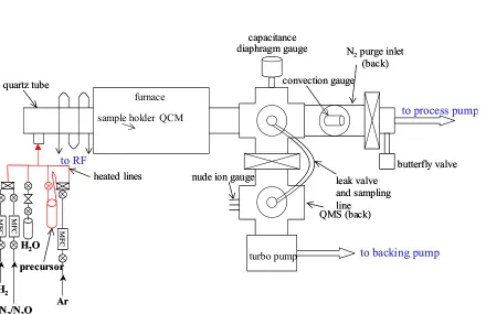
Films preparationALD Ru and Rh processes were carried out in a home-built hot-wall quartz tube reactor
shown in Figure 1.3 using RuCp2 (bis-(cyclopentadienyl)ruthenium) and Rh(acac)3
(rhodium acetylacetonate) as a precursor, respectively. Dry oxygen was used as reactant for
both processes. RuCp2 andRh(acac)3 are solid at room temperature with vapor pressure of
~10mTorr at the bubbler temperature of 80°C and vapor pressure ~20mTorr at the bubbler
temperature of 150°C, respectively. The ALD chamber was evacuated to 5x10⁻⁶ Torr, and the precursor and oxidant gases were introduced into the reactor in separate pulses with an
pulse and purity of Ar is 99.999%. During the deposition, the total gas flow rate was
constant at 100~300sccm, deposition temperature was 275~350°C, and the chamber was
dynamically pumped to maintain pressure at 0.9~1.2 Torr. Flow rate was controlled by
needle valve and mass flow controller was not used in this study. Gas line before furnace
was kept at 100°C and 160°C with heating tapes for ALD Ru and Rh process, respectively.
The valve after precursor cells (bubblers) were always kept at 60~80°C and 150°C to
prevent precursors’ condensation at the valve. In case of Rh, since Rh(acac)3 has high
sublimation temperature, precursor condensation is very sensitive to a cold spot in the gas
line and valve. Pressure deviation between precursor dose step and Ar gas purge step can
indicate precursor condensation in gas line or valve. Compare to Ar purge, precursor dose
step shows much smaller pressure suggesting precursor condensation. For substrate holder,
7-inch quartz boat having 5 different positions or 4-inch aluminium boat having 3 different
positions was used. During experiment substrate front side of holders were placed at
~3inch and ~5inch inside from furnace inlet for quartz and aluminium boat, respectively. In
case of Ru, deposited film was the thickest at second position of quartz boat. This suggests
that gas temperature is stabilized at 2nd position and precursor is depleted along with
furnace tube length. Unlike Ru, at ALD Rh process due to precursor’s, Rh(acac)3, high
vapor pressure and its intrinsic properties, precursor depletion was detected at 5th position. Rh films at 3rd and 4th position were the thickest and film at 1st position was thinner than 2nd position indicating temperature deviation of gas between furnace inlet and inside. After
load samples on substrates into furnace before each ALD process starts, ~30min. was taken
cycle was Ar 20-precursor 3-Ar 20-oxygen 6 and Ar 15-precursor 15-Ar 15-oxygen 10 for
ALD Ru and Rh, respectively. When sample is unloaded from furnace, N2 gas was used
during system vent process. As substrate, chemical silicon oxide, thermal oxide,
H-terminated silicon, PVD hafnium oxide, CVD hafnium oxide, and CVD HfSiOx were used.
To prepare substrates, silicon surfaces were oxidized by wet chemical treatment
(BakerClean® JTB-100), followed by buffered HF acid dip, deionized water rinse, and N2
flow dry. Silicon was either directly oxidized to form SiO2, (900ºC in air) or coated with
thin Hf films by sputtering, followed by thermal oxidation. A micro-slide glass was used to
mask parts of substrate to make step through which thickness can be measured using
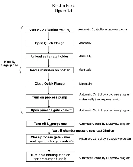
profilometer. Experimental schematic of films preparation using thermal ALD equipment
is shown in Figure 1.4. CVD hafnium oxide and hafnium silicate as substrates were
provided from Texas Instrument and Sematech. Film continuity was checked to examine
metal deposition using voltmeter before further analysis. Deposited film thicknesses were
measured using a Tencor Alpha-Step 500 surface profilometer. Film resistivities were
measured using 4-point probe station.
Materials charaterization
1) X-Ray Photoelectron Spectroscopy (XPS)
XPS was used to determine the chemical states and impurities present in the deposited
films. XPS operates by exposing the sample to x-ray photons, causing photoelectron
emission from specific energy levels which are characteristic of the elements present in the
energies (which relate to binding energies) correspond to specific elements, thus indicating
the presence of impurities such as possible carbon contamination from metallorganic
precursors. Peaks corresponding to individual energy levels can also shift to different
binding energies depending on the local bonding environments of the atoms involved, and I
will use these chemical shifts to determine the oxidation states of species in the deposited
films.63-65 The primary drawback of XPS is its low throughput, since the analysis chamber must be pumped down to UHV conditions.
Most of XPS analysis were conducted with a system that uses a MgK X-ray source to
produce 1253.6 eV photons, and has a resolution of 0.5 eV, detection limit of about 0.5
at%, and sampling depth of up to 100 Å.
2) Fourier Transform Infrared Spectroscopy (FTIR)
To complement the XPS, FTIR was used for fast characterization of the chemical states of
impurities present in the deposited films. This technique operates by exposing the sample
to an IR beam and recording the frequencies absorbed by the sample, which correspond to
the specific molecular vibrational frequencies of the chemical species present. While less
useful for analysis of metals and their oxidation states than XPS, FTIR is more useful for
analysis of impurities and their bonding environments, and impurities such as carbon,
nitrogen, and hydroxyl groups (possibly due to H2O uptake) can be readily studied. A
Thermo-Nicolet Magna-750 IR spectrometer with a detection limit of about 1 at% and
detectable wavelengths from 400-4,000 Å was used for this research. Some drawbacks of
examine peaks for metallic species such as hafnium compounds in the available frequency
range (although far-IR characterization may also be available through collaborations with
other research groups).64,66-68
3) Auger Electron Spectroscopy (AES)
As another surface analysis tool, AES was used to measure chemical compositions of
deposited films. AES operates by exposing the sample to an incident electron beam,
causing emission of Auger electrons from higher energy levels when a core hole is filled.
As with XPS, peaks in the kinetic energy spectrum of the emitted electrons correspond to
characteristic energy levels of specific elements, thus indicating the presence and relative
concentrations of those elements in the sample. However, unlike XPS, relative
concentrations are more easily quantified (although less chemical state information is
obtained) and the technique is more effectively coupled with ion sputtering, a destructive
depth-profiling technique in which the sample surface is eroded away by ion bombardment
to characterize changes in chemical composition with depth (generally with a depth
resolution as low as 5 Å).21,65,67,69
4) Atomic Force Microscopy (AFM)
To determine the root mean square (RMS) roughness and uniformity of the deposited films,
AMF was used. AFM operates by bringing a cantilever-mounted probe tip close enough to
the sample surface so that interatomic forces repel the tip, which is scanned across the
polycrystalline film morphology (possibly indicating the grain size), and the surface
roughness can be quantitatively measured through calculation of the RMS roughness. This
research utilized a Digital Instruments DI3 model AFM with silicon Veeco Nanoprobe tips
(5-10 nm radius of curvature), and RMS roughness values was extracted from 1µm square
scans conducted in tapping mode. Since ALD films are inherently smooth and uniform,
uniformly low RMS roughness values (possibly remaining as low as 4-10 Å for films less
than 500 Å thick, depending on the material and its morphology)70 over an entire sample
surface would indicate true ALD growth, while non-uniformity and higher roughness
values could indicate incomplete dosing of reactants, poor nucleation, or polycrystalline
grain growth.19
Electrical Characterization
To electrically characterize metal films deposited by ALD, MOS capacitors were fabricated
and performed capacitance-voltage (C-V) measurements on them using an HP 4283A LCR
meter. To characterize ALD metal films, metal was deposited on thermal SiO2 and Hi-k
dielectric on p-type Si (100) wafers, then Al was deposited by evaporation on the top of
ALD metal through a shadow mask and the backside of the Si sample to form the electrical
contacts of the 2-terminal MOS capacitor structure. The shadow mask patterned capacitor
gate dots having areas ranging from 10-5-10-3 cm2. Then ALD metal was etched off using the Al dots as a hard resist. In case of Ru, reactive ion etching was used and condition was
When capacitance vs. voltage sweeps were performed at different frequencies (about 1 kHz
can be made about the equivalent oxide thickness (EOT), the presence of charge in the
oxide, and effective work function of ALD metal. In general, the flatband voltage obtained
from the C-V curves shifts to more negative voltages with the presence of positive oxide
fixed or trapped charges, and to more positive voltages with the presence of negative oxide
fixed or trapped charges. Shifts are identified by comparing the observed flatband voltage
(VFB) to an “ideal” value of VFB = φs - φm, where φs and φm are the effective work functions
of the semiconductor and the gate metal, respectively. To extract parameters such as VFB,
EOT, oxide capacitance (Cox), flatband capacitance (CFB), a curve-fitting program
developed by Prof. J.R. Hauser at NCSU was used71 From EOT vs. VFB obtained from C-V
analysis, the effective metal work function was extracted from the intercept of above
equation.
1.7 Overview of dissertation
This dissertation has been focused on understanding ALD noble metals processes,
nucleations, electrical and material properties as well as interface properties at
metal/dielectric CMOS metal gate electrode applications. ALD Ru and Rh processes have
been demonstrated sucessfully using thermal ALD on various dielectrics. ALD Ru
nucleation behaviors were studied and novel area-selective deposition was demonstrated to
extend of nucleation study. The effective work functions of ALD Ru and Rh were noticed
to be different, which may be due to interface dipole either from intrinsic and extrinsic
shown to be tunable. ALD growth model on H-terminated Si surface was studied and
theoretical and experimental data were shown.
Chapter 2 describes demonstration of novel area selective ALD Ru deposition. The growth
rate of ALD Ru is similar on various starting surfaces, but the growth initiation differed
substantially. Patterned organic monolayers are used to inhibit film nucleation, enabling
selective area atomic layer deposition (ALD) of ruthenium on SiO2 and HfO2 surfaces. It
was confirmed that OTS could deactivate film growth on thermal silicon oxide and hafnium
oxide surfaces by X-ray photoelectron spectroscopy (XPS). Metal-oxide-semiconductor
capacitors were fabricated directly using the selective-area process.
Chapter 3 discusses a thermal process for ALD of rhodium using Rhodium(III)
acetylacetonate and dry oxygen. The resistivity and XPS of Rh films were measured
indicating metallic Rh. Capacitors were formed by selective area ALD of Rh onto SiO2 and
HfO2 substrates. The effective work function as-deposited ALD Rh films were measured
and observed to be higher on SiO2 than on HfO2 dielectrics.
Chapter 4 presents Organic self-assembled monolayers formed on SiO2 and high-k
dielectric surfaces on silicon can be used to modify the effective work function of
ruthenium metal films deposited onto the organic layer by atomic layer deposition (ALD).
Capacitance measurements of the resulting metal/dielectric/seminconductor stack show that
the effective work function of the Ru can decrease by up to 0.6eV, and increase 0.2eV
depending on the nature of the organic monolayer.
Chapter 5 we demonstrate the nucleation behaviors of Ru metal films deposited by ALD.
found that hydrophilicity surfacee gives shorter nucleation incubation period than
hydrophobic surface time with similar growth rate. ALD Ru nucleation characteristics on
H-terminated Si and thermal SiO2 during the incubation time were studied by XPS and
AFM. ALD Ru film showed good thermal stability even after 1000°C annealing from SEM
analysis comparing surface structure with as-deposited film. ALD Ru film was found
polycrystalline having (002) primary structure on HfO2 and thermal SiO2 and (101) on
HfSiOx.
Chapter 6 presents results of Ru ALD nucleation on H-terminated silicon surface using
XPS and AFM analysis. Silicon oxide formation was confirmed during ALD cycles from
observing emerging Si2p even after 10ALD cycles. Film thickness was measured from
XPS Ru3d peak values showing growth rate transient region exists. AFM roughness
analysis of ALD Ru films is consistent with growth rate changing upto 100ALD cycles.
Based on experimental data, simple ALD growth model was established. It was noticed that
Reference
1 C. H. L. Goodman and M. V. Pessa, J. Appl. Phys. 60, R65 (1986). 2 T. Suntola, A. J. Pakkala, and S. Lindfords, SID 80 Dig. 11, 108 (1980). 3 T. Suntola, Thin Solid Films 216, 84 (1992).
4 T.Suntola and J. Hyvarinen, Annu. Rev. Mater. Sci. 15, 177 (1985). 5 J. Nishzawa and T. Kurabayashi, Thin Solid Films (2000).
6 S. M. Bedair, J. Vac. Sci. Technol. B 12, 179 (1994).
7 H. S. Nalwa,
Handbook of Thin Film Materials.
8 T. Suntola, Applied Surfce Science 100/101, 391-398 (1996). 9 T. Suntola and D. T. J. Hurle,
Handbook of Crystal Growth, Vol. 3 (1994). 10 M. Ylilammi, J. Electrochem. Soc. 142, 2474-2479 (1995).
11 M. Ylilammi, Thin Solid Films 279, 124-130 (1996).
12 M. K. Gobbert, V. Prasad, and T. S. Cale, Thin Solid Films 410, 129-141 (2002).
13 J. B. Hudson,
Surface Science: An Introduction. (John Wiley & Sons, New York,
1998).
14 M. A. Herman, Applied Surfce Science 112, 1-11 (1997). 15 A. E. Braun, Semiconductor International, 52-58 (2001). 16 M. Ritala and M. Leskela, Nanotechnology 10, 19-24 (1999).
17 M. Leskela and M. Ritala, Journal de Physique IV 9, Pr837-Pr852 (1999).
18 D.-G. Park, K.-Y. Lim, H.-J. Cho, T.-H. Cha, I.-S. Yeo, J.-S. Roh, and J. W. Park,
Applied Physics Letters 80, 2514 (2002).
20 L. Niinisto, Solid State & Materials Science 3, 147-152 (1998). 21 J. D. Plummer, M. D. Deal, and P. B. Griffin,
Silicon VLSI Technology:
Fundamentals, Practice, and Modeling (Prentice Hall, Upper Saddle River, New
Jersey, 2000).
22 H. Kim, C. J. Cabral, C. Lavoie, and S. M. Rossnagel, Journal of Vacuum Science
and Technology B 20, 1321-1326 (2002).
23 S. M. Rossnagel, Journal of Vacuum Science and Technology B 18, 2016-2020
(2000).
24 M. Ritala, P. Kalsi, D. Riihela, K. Kukli, M. Leskela, and J. Jokinen, Chemistry of
Materials 11, 1712-1718 (1999).
25 P. Alen, M. Juppo, M. Ritala, T. Sajavaara, J. Keinonen, and M. Leskela, Journal of
Electrochemical Society 148, G566-G571 (2001).
26 J. S. Park, M. J. Lee, C. S. Lee, and S. W. Kang, Electrochemical and Solid-State
Letters 4, C17-C19 (2001).
27 J. Koo, J. W. Lee, T. Doh, Y. Kim, Y. D. Kim, and H. Jeon, Journal of Vacuum
Science and Technology A 19, 2831-2834 (2001).
28 M. Juppo, P. Alen, M. Ritala, T. Sajavaara, J. Keinonen, and M. Leskela,
Electrochemical and Solid-State Letters 5, C4-C6 (2002).
29 J.Uhm and H. Jeon, Japanese Journal of Applied Physics 40, 4657-4660 (2001). 30 G. D. Wilk, R. M. Wallace, and J. M. Anthony, Journal of Applied Physics 89,
5243-5275 (2001).
32 C. H. Lee, H. F. Luan, W. P. Bai, S. J. Lee, T. S. Jeon, Y. Senzaki, D. Roberts, and
D. L. Kwong, IEDM Technology Digest, 27-30 (2000).
33 D. C. Gilmer, R. Hegde, R. Cotton, R. Garcia, V. Dhandapani, D. Triyoso, S. Roan,
A. Franke, R. Rai, L. Prabhu, C. Hobbs, J. M. Grant, L. La, S. Samavedam, B.
Taylor, H. Tseng, and P. Tobin, Applied Physics Letters 81, 1288-1290 (2002).
34 K. Frohlich, K. Husekova, D. Machajdik, J. C. Hooker, N. Perez, M. Fanciulli, S.
Ferrari, C. Wiemer, A. Dimoulas, G. Vellianitis, and F. Roozeboom, Materials
Science and Engineering B 109, 117-121 (2004).
35 B. Cheng, M. Cao, R. Rao, A. Inani, P. V. Voorte, W. M.Greene, J. M. C. Stork, Z.
Yu, P. M. Zetzoff, and J. C. S. Woo, IEEE Transactions on Electron Devices 46 7,
1537-1544 (1999).
36 Y. C. Yeo, P. Ranade, T. J. King, and C. Hu, IEEE Electron Device Letters 23,
342-344 (2002).
37 Q. Lu, R. Lin, P. Ranade, T. J. King, and C. Hu, Symposium on VLSI Technology
Digest of Technical Papers, 45-46 (2001).
38 Y. C. Yeo, Q. Lu, P. Ranade, H. Takeuchi, K. J. Yang, I. Polishchuk, T. J. King, C.
Hu, S. C. Song, H. F. Luan, and D.L. Kwong, IEEE Electron Device Letters 22,
227-229 (2001).
39 H. Zhong, G.Heuss, and V. Misra, IEEE Electron Device Letters 21, 593-595
(2000).
40 Y. Abe, Y. Kaga, M. Kawamura, and K. Sasaki, Journal of Vacuum Science and
41 Y. Kaga, Y. Abe, M. Kawamura, and K. Sasaki, Japanese Journal of Applied
Physics 38, 3689-3692 (1999).
42 J. M. Lee, J. C. Shin, C. S. Hwang, H. J. Kim, and C. G. Suk, Journal of Vacuum
Science and Technology A 16, 2768-2771 (1998).
43 S. K. Hong, H. J. Kim, and H. G. Yang, Journal of Applied Physics 80, 822-826
(1996).
44 T. Yunogami and K. Nojiri, Journal of Vacuum Science and Technology B 18,
1911-1914 (2000).
45 J. G. Lee, Y. T. Kim, S. K. Min, and S. H. Choh, Journal of Applied Physics 77,
5473-5475 (1995).
46 S. E. Park, H. M. Kim, K. B. Kim, and S. H. Min, Thin Solid Films 341, 52-54
(1999).
47 Y. S. Huang and P. C. Liao, Solar Energy Materials and Solar Cells 55, 179-197
(1998).
48 T. Aoyama and K. Eguchi, Japanese Journal of Applied Physics 38, 1134-1136
(1999).
49 J. H. Lee, J. Y. Kim, and S. W. Rhee, Electrochemical and Solid-State Letters 2,
622-623 (1999).
50 K. C. Smith, Y. M. Sun, N. R. Mettlach, R. L. Hance, and J. M. White, Thin Solid
Films 376, 73-81 (2000).
51 J. Sanka, T. K. Sham, and R. J. Puddephatt, Journal of Materials Chemistry 9,
52 S. E. Park, H. M. Kim, K. B. Kim, and S. H. Min, Journal of Electrochemical
Society 147, 203-209 (2000).
53 M. H. Tsai, S. C. Sun, H. T. Chiu, C. E. Tsai, and S. H. Chuang, Applied Physics
Letters 67, 1128-1130 (1995).
54 Y. S. Suh, G. Heuss, H. Zhong, S. N. Hong, and V. Misra, Symposium on VLSI
Technology Digest of Technical Papers, 47-48 (2001).
55 V. Misra, G. P. Heuss, and H. Zhong, Applied Physics Letters 78, 4166-4168
(2001).
56 I. Polishchuk, P. Ranade, T. J. King, and C. Hu, 4 200-202 (2002).
57 I. Polishchuk, P. Ranade, T. J. King, and C. Hu, IEEE Electron Device Letters 22,
444-446 (2001).
58 V. Misra, H. Zhong, and H. Lazar, IEEE Electron Device Letters 23, 354-356
(2002).
59 P. Martensson and J. O. Carlsson, Applied Surfce Science 148, 9-16 (1999). 60 P. Martensson and J. O. Carlsson, Chemical Vapor Deposition 3, 45-50 (1997). 61 Y. B. Kim, M. Tuominen, I. Raaijmakers, R. d. Blank, R. Wilhelm, and S. Haukka,
Electrochemical and Solid-State Letters 3, 346-349 (2000).
62 M. L. Green, M.-Y. Ho, B. Busch, G. D. Wilk, T. Sorsch, T. Conard, B. Brijs,
W.Vandervorst, P. I. Raisanen, D. Muller, M. Bude, and J. Grazul, Journal of
Applied Physics 92, 7168 (2002).
63 T. L. Barr,
64 J. P. Sibilia,
A Guide to Materials Characterization and Chemical Analysis
(Wiley-VCH, New York, 1996).
65 D. P. Woodruff and T. A. Delchar,
Mordern Techniques of Surface Science
(Cambridge University Press, Cambridge, U.K., 1994).
66 R. M. Silverstein and F. X. Webster,
Spectrometric Identification of Organic Compounds (John Wiley & Sons, Inc., New York, 1998).
67 D. K. Schroder,
Semiconductor Materials and Device Characterization (John Wiley
& Sons, Inc., New York, 1998).
68 Y. J. Chabal, Surface Science Reports 8, 211-357 (1988). 69 D. Briggs and M. P. Seah,
Practical Surface Analysis (Second Edition) Volume1-Auger and X-ray Photoelectron Spectroscopy (John Wiley & Sons Inc., New York,
1996).
70 J. W. Elam, Z. A. Sechrist, and S. M. George, Thin Solid Films 414, 43-55 (2002). 71 J. R. Hauser and K. Ahmed, edited by D. G. Seiler (AIP, New York, 1998), p.
Figure caption:
Figure 1.1 The schematic of ALD process in the simplest case
Figure 1.2 (a) The energy band diagram of a N-MOS device showing the depletion layer in
the poly-Si gate. (b) The poly-Si gate depletion effect decreases the gate capacitance in the
inversion regime as evident in the capacitance-voltage plot. Taken from reference 31
Figure 1.3 The schematic of home-built hot-wall quartz tube ALD reactor
Kie Jin Park
Figure 1.1
Argon Purge
Argon Purge
ligand desorption ligand desorption
Argon Purge Argon Purge
Argon Purge Argon Purge
Kie Jin Park
Figure 1.2
n+poly-Si
gate dielectric p-Si substrate Ec EV EF,gate Ec EV EF,s
Poly-Si gate depeletion layer thickness
Voltage drop across depeletion layer
Inversion charge
n+poly-Si
gate dielectric p-Si substrate Ec EV EF,gate Ec EV EF,s
Poly-Si gate depeletion layer thickness
Voltage drop across depeletion layer Inversion charge 1.0 0.8 0.6 0.4 0.2 0.0 4 2 0 -2
No gate depletion
With gate Depletion effect Inversion regime Accumulation regim e
C
a
pa
c
it
a
nce
(
µ
F/
cm
2)
Gate Voltage VG(V)
1.0 0.8 0.6 0.4 0.2 0.0 4 2 0 -2 1.0 0.8 0.6 0.4 0.2 0.0 4 2 0 -2 1.0 0.8 0.6 0.4 0.2 0.0 4 2 0 -2
No gate depletion
With gate Depletion effect Inversion regime Accumulation regim e
C
a
pa
c
it
a
nce
(
µ
F/
cm
2)
Gate Voltage VG(V)
Kie Jin Park
Figure 1.3
to RF
furnace
sample holder QCM
quartz tube convection gauge
N2purge inlet
(back)
butterfly valve
to process pump
leak valve and sampling line
nude ion gauge
QMS (back)
turbo pump to backing pump capacitance diaphragm gauge MF C MF C H2 N2/N2O
H2O
MF C Ar precursor heated lines to RF furnace
sample holder QCM
quartz tube convection gauge
N2purge inlet
(back)
butterfly valve
to process pump
leak valve and sampling line
nude ion gauge
QMS (back)
turbo pump to backing pump capacitance diaphragm gauge MF C MF C H2 N2/N2O
H2O
MF
C
Ar precursor
Kie Jin Park
Figure 1.4
Vent ALD chamber with N2
Open Quick Flange
Automatic Control by a Labview program
Unload substrate holder
Mannually
Mannually
load substrates on holder Mannually
Close Quick Flange Mannually
Turn on process pump
Keep N2 purge gas on
Automatic Control by a Labview program + Mannually turn on power switch
Open process gate valve Automatic Control by a Labview program
Vent ALD chamber with N2
Open Quick Flange
Automatic Control by a Labview program
Unload substrate holder
Mannually
Mannually
load substrates on holder Mannually
Close Quick Flange Mannually
Turn on process pump
Keep N2 purge gas on
Automatic Control by a Labview program + Mannually turn on power switch
Open process gate valve*1 Automatic Control by a Labview program
Turn off N2 purge gas Automatic Control by a Labview program
Close process gate valve
and open turbo gate valve Automatic Control by a Labview program
Wait till chamber pressure gets least 25mTorr
Turn on a heating tape on
for precursor bubble Automatic Control by a Labview program
Turn off N2 purge gas Automatic Control by a Labview program
Close process gate valve
and open turbo gate valve Automatic Control by a Labview program
Wait till chamber pressure gets least 25mTorr
Turn on a heating tape on
for precursor bubble Automatic Control by a Labview program
Wait for 30min.
Close turbo gate valve and open process gate valve
Immediately
Turn process start on
Automatic Control by a Labview program Program default allows Ar flow for 30 sec.
Change butterfly valve switch to automatic
and program dose times and ALD cycle
Mannually
Wait for 30min.
Close turbo gate valve and open process gate valve
Immediately
Turn process start on
Automatic Control by a Labview program Program default allows Ar flow for 30 sec.
Change butterfly valve switch to automatic
and program dose times and ALD cycle
Mannually
Turn on process start on
Wait till Ar process completes
Automatic Control by a Labview program
Change butterfly valve switch to open
Wait till ALD process completes (process automatically finishes)
Wait till chamber pressure gets least 25mTorr
Close process gate valve
and open turbo gate valve Automatic Control by a Labview program
Wait for 1min.
Close turbo gate valve Automatic Control by a Labview program
Vent ALD chamber with N2 Automatic Control by a Labview program
*1: Process gate valve: Gate valve to process pump
Chapter 2 is a reprint of a manuscript published in Applied Physics Letters,
CHAPTER 2. Microcontact Patterning of Ruthenium Gate
Electrodes by Selective Area Atomic Layer Deposition
K.J. Park
a, J.M. Doub, T. Gougousi, and G.N. Parsons
Department of Chemical and Biomolecular Engineering
North Carolina State University
Raleigh, NC 27695
Abstract
Patterned octadecyltrichlorosilane monolayers are used to inhibit film nucleation, enabling
selective area atomic layer deposition (ALD) of ruthenium on SiO2 and HfO2 surfaces
using bis-(cyclopentadienyl)ruthenium and oxygen. X-ray photoelectron spectroscopy
indicated that OTS could deactivate film growth on thermal silicon oxide and hafnium
oxide surfaces. The growth rate of ALD Ru is similar on various starting surfaces, but the
growth initiation differed substantially. Metal-oxide-semiconductor capacitors were
fabricated directly using the selective-area process. Capacitance measurements indicate the
effective work function of ALD Ru is 4.84±0.1eV on SiO2, and the effective work function
2.1 Introduction
Improved control of interface reactions during thin film processing is critical for
advanced electronic and optical devices. Ruthenium is of interest for advanced
metal/oxide/semiconductor (MOS) transistor gate electrodes to reduce poly-silicon
depletion effects and as nucleation layer for copper interconnect layers.1 Ruthenium is considered a viable candidate for p-type MOS devices because it has a vacuum work
function near the conduction band edge of silicon, good thermal stability, and low
resistivity of the oxidation phase.2
Microcontact-printed organic monolayer resists have previously been used for selective
area atomic layer deposition (ALD) of oxides3-5 and for chemical vapor deposition (CVD) of metals.6 A previous report demonstrates selective area digital CVD Ru using patterned photoresist.7 In this work, selective deposition of Ru is demonstrated using contact printed self assembled monolayer resists by ALD processing. Also in this work, spectroscopic
characterization is used to demonstrate selectivity, and the effect of processing on the
monolayer structure is analyzed. Selective deposition enables direct formation of
Ru/HfO2(SiO2)/Si capacitor stacks, and the effective work function of ALD Ru is
characterized on HfO2 and SiO2 dielectrics. A key problem for metals in CMOS is
methodology to enable integration of two different metal work functions. Techniques to
integrate two different metals in nanoscale device fabrication include selective modification
2.2 Experimental
ALD Ru was carried out in a home-built hot-wall quartz tube reactor using RuCp2
(bis-(cyclopentadienyl)ruthenium) as a precursor and dry oxygen. RuCp2 issolid at room
temperature with vapor pressure of ~10mTorr at the bubbler temperature of 80°C. To
prepare substrates, silicon surfaces were oxidized by wet chemical treatment (BakerClean® JTB-100), followed by buffered HF acid dip, deionized water rinse, and N2 flow dry.
Silicon was either directly oxidized to form SiO2, (900ºC in air) or coated with thin Hf
films by sputtering, followed by thermal oxidation. For example, the Hf based films with
equivalent oxide thickness (EOT) of 30Å consisted of 11Å of sputtered hafnium followed
by oxidized in N2 (with ~20ppm O2) at 600ºC for 1 min.12 These conditions likely resulted
in growth of HfO2 with some interfacial HfSiOx and/or SiO2. The samples are referred to
here as HfO2/SiO2 films.
To prepare the patterned organic monolayer an elastomeric stamp was made of
polydimethylsiloxane (PDMS) solution and a curing agent. The mold patterns for the
PDMS stamps were micron-scale line/space photoresist and metallic dots made by physical
vapor deposition of aluminum through a shadow mask. A solution of OTS
(octadecyltrichlorosilane) in dry hexane (10mM) was used as the “ink”. The OTS solution
was applied to the PDMS stamp by spin coating, and the inked stamp was dried in nitrogen
flow for 30s. The stamp was then brought into contact with the clean substrate and held in
place for 30-60s. The resulting OTS films were characterized by water contact angle
analysis, scanning force microscopy and X-ray photoelectron spectroscopy (XPS). For
its solution at room temperature. Resulting films showed a static contact angle with water
to be between <90 and 110º, consistent with a range of film quality, from relatively poorly
packed (<90º), to highly packed (110º) films.13,14 Films with contact angle ≥ 90° show similar results in inhibiting deposition. After exposure to 300 cycles of Ru ALD, the OTS
monolayers generally showed reduced contact angle (<80º), indicating monolayer
degradation. The results suggest that Ru nucleation is not as sensitive to quality of the
monolayer surface as observed for Hf or Zr oxide15 and Ti based 13 film deposition. This may be due to the higher oxygen affinity of Hf, Zr, and Ti where these metals are more
likely to penetrate the monolayer and react with oxide present at the Si/monolayer interface.
The OTS-patterned substrates were rinsed in hexane and deionized water, then dried with
nitrogen flow before being loaded into the ALD reactor. The ALD chamber was evacuated
to 5x10⁻⁶ Torr, and the precursor and oxidant gases were introduced into the reactor in separate pulses (3 and 6 sec, respectively) with a 20 second Ar purge between each reactant.
Argon was also used as a carrier gas for the RuCp2 pulse. During the deposition, the total
gas flow rate was constant at 100sccm, and the chamber was dynamically pumped to
maintain pressure at 1.2 Torr. Under these conditions, self limiting growth was observed at
temperatures between ~310º and 350ºC corresponding to ~1Å per deposition cycle, which
is larger that 0.5A/cycle reported previously for Ru ALD.16 This difference is under investigation. The resulting Ru films were characterized by surface profilometry to
determine thickness, and XPS was used to determine the film chemical composition.
Capacitance vs. voltage (CV) was measured using an HP 4284A LCR meter at 1MHz using
2.3 Results and Discussion
Figure 2.1 shows Ru film thickness vs number of ALD cycles for deposition on HfO2/SiO2,
SiO2, and hydrogen-terminated silicon (HF-last) surfaces. For deposition on the HF-last,
no film was observed by eye after 100 cycles for the conditions used. Also, on the OTS
surface, no film was observed by XPS (vide infra) for up to 300 cycles studied. The inset
in Figure 2.1 is an optical image of a selectively deposited Ru capacitor on HfO2/SiO2
using the OTS monolayer resist. The deposited thickness per cycle was similar on SiO2,
HfO2/SiO2, and Si-H, but the intercepts show different values, consistent with different
incubation times for growth on these surfaces. However, details of growth incubation
require more investigation of thin (<100Å) layer growth.17 Figures 2.2(a) and 2(b) show XPS spectra after 150 cycles of selective ALD Ru at 325 °C on clean SiO2 and on SiO2
covered with microcontact-stamped OTS. Figure 2(b) shows that the Ru 3p peaks are not
observed on the OTS covered regions after ALD, indicating good selectivity to Ru growth
with this monolayer surface (static contact angle for this sample was 92° before Ru
deposition). The measured Ru 3p1/2 and 3p3/2 peak positions at 484 and 462eV, and the width of the peaks are consistent18 with the presence of several Ru oxidation states from elemental Ru to mildly oxidized RuOx. Presence of RuOx is confirmed by the existence of
the O1s peak, although it is possible that most of the O in confined to the surface. Because
of overlap of C1s and Ru3d peaks, it is difficult to calibrate the XP spectrum energy scale
to compensate for surface charge. The spectrum from the Ru film shows a small signal