ABSTRACT
TERRY, DAVID B. A holistic investigation of alternative gate stack materials for future
CMOS applications. (Under the direction of Dr. Gregory N. Parsons.)
High dielectric constant (high-k) insulators and metal gate electrodes are important
for advanced MOS devices to limit gate leakage by increasing gate capacitance with ultimately thicker films and eliminate poly-depletion & dopant diffusion, respectively. Reactions between dielectric/substrate and gate electrode/dielectric during deposition or
post-deposition processing lead to an increase in interfacial layer formation, and the mechanisms that control the changes need to be well understood. We investigate yttrium-based and
hafnium-based high-k dielectrics and ruthenium-based gate electrodes formed by various processing methods such as physical vapor deposition (PVD), chemical vapor deposition (CVD), and atomic layer deposition (ALD) on Si(100). Characterization techniques include
IR, XPS, TEM, EELS, AES, and IV and CV electrical analysis. During deposition and post-deposition treatments the interfaces have some extent of interfacial layer formation. The
extent of the intermixing depends on substrate surface preparation, process conditions, and annealing conditions. The transition metal alluminate dielectrics show evidence on flatband voltage tuning via charge compensation. Also, the ruthenium gate electrodes show that
process condition can have a direct effect the electronic and chemical properties of MOS structures such as in-situ versus ex-situ capacitor fabrication and the role of subsurface
A holistic investigation of alternative gate stack materials for
future CMOS applications
by
David B. Terry
A dissertation submitted to the Graduate Faculty of North Carolina State University
In partial fulfillment of the Requirements for the Degree of
Doctor of Philosophy
CHEMICAL ENGINEERING
Raleigh, North Carolina 2006
APPROVED BY:
Dr. Gregory N. Parsons Chair of Advisory Committee
Dr. Orlin Velev Dr. Carl Osburn
This thesis is dedicated to: my Daughter, Elaina Santana Skipper, my parents, James E. Terry and Kathleen L. Terry,
Biography
David B. Terry was born June 16, 1970 in Lancaster, Pennsylvania. He grew up in Wilmington, North Carolina and graduated from New Hanover High School. He join the United States Air Force from 1990-1993 with a job in communication were he relayed,
received, and transmitted TOP SECRET messages. He majored in Chemistry, and received a Bachelor of Science degree with honors in 1999. He enrolled in the Chemical Engineering graduate program at North Carolina State University in August 1999. Upon completion of
ACKNOWLEDGEMENTS
I am grateful to my advisor Dr. Gregory N. Parsons for his continuous guidance and support throughout this work. He also has been a great mentor and a true friend to me. I am
thankful to the past and present members in Dr. Parsons’ group, Dr. Dong Niu for training me on the CVD system, Dr. Atul Gupta, Dr. Elisa Rosa, Dr. Kevin Bray, Dr. Jason Kelly, Dr.
Kiejin Park, and Qing Peng, Jeong-Seok Na, Joe Spagnola, Jason Doub, Rob Ashcraft, Scott Burnside, Katherine Schadel, and Michael Stewart for thoughtful discussions and collaborations. I would like to give a special thanks to Dr. Changwoong Chu for being a
great friend and colleague who has helped me through many of the challenges that I have faced during my tenure as a graduate student and to Dr. Theodosia Gougousi for being such a
wonderful mentor and friend.
I would like to acknowledge my committee members, Dr. Jan Genzer, Dr. Carl Osburn, and Dr. Orlin Velev for their support and excellent mentoring. I would also like to
thank my collaborators, Dr. Misra, Dr. Garfunkel, Dr. J.-P. Maria, Dr. Goncharova for performing various analysis.
Special thanks to Kit Yeung for being a good friend and helping me repair and maintain of the CVD system. Also thanks to the cleanroom staff personnel including Joan O’Sullivan, Dr. Ginger Yu, and Henry Taylor. Thanks to all the people at AIF, especially
Table of Contents
LIST OF FIGURES ... vii
CHAPTER 1 INTRODUCTION... 1
HISTORICAL PERSPECTIVE... 1
COMPLEMENTARY METAL OXIDE SEMICONDUCTOR... 2
OBJECTIVE OF THIS WORK... 3
OVERVIEW OF DISSERTATION... 4
REFERENCES... 7
CHAPTER 2 METAL GATE CMOS TECHNOLOGY... 10
ADVANCED GATE ELECTRODE MATERIALS... 10
SELECTION OF MATERIALS... 14
CANDIDATE MATERIALS... 15
Physical Properties... 16
Work Function ... 19
METAL GATE/HIGH-K DIELECTRIC INTEGRATION... 20
PROCESS INTEGRATION... 22
Dual Metal Gate CMOS Technology... 22
Metal Interdiffuion Gate CMOS Technology... 24
WORK FUNCTION ENGINEERING... 26
Structural Modification... 26
Chemical Modification... 27
REFERENCES... 29
CHAPTER 3 DEPOSITION AND CHARACTERIZATION TECHNIQUES ... 33
ATOMIC LAYER DEPOSITION (ALD)... 33
Introduction... 33
ALD process... 33
Intrinsic Advantages of ALD... 36
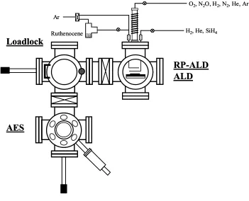
PALD REACTOR... 37
FILM CHARACTERIZATION... 38
On-line Auger Electron Spectroscopy (AES)... 38
Fourier Transform Infrared Spectroscopy (FT-IR) ... 39
X-ray Photoelectron Spectroscopy (XPS)... 39
Rutherford Backscattering Spectroscopy (RBS) ... 40
Transmission Electron Microscopy (TEM)... 40
Surface Profilometry... 41
Ellipsometry ... 42
Electrical measurement on MOS Capacitors ... 42
REFERENCE... 44
CHARGE COMPENSATION AND THERMAL STABILITY OF (HFO2)X(AL2O3)1-X AND (Y2O3)X(AL2O3)1-X FORMED BY OXIDATION OF HFX:AL1-X AND YX:AL1-X
MIXTURES ON SI ... 48
INTRODUCTION... 49
EXPERIMENTAL APPROACH... 53
RESULTS AND DISCUSSION... 54
CONCLUSIONS... 57
CHAPTER 5... 69
CHEMICAL VAPOR DEPOSITION OF RUO2 FOR GATE ELECTRODE APPLICATIONS ... 69
INTRODUCTION... 71
EXPERIMENTAL APPROACH... 73
RESULTS AND DISCUSSION... 75
CONCLUSIONS:... 79
REFERENCES... 80
CHAPTER 6... 90
CHARGE GENERATION DURING OXIDATION OF THIN HF METAL FILMS ON SILICON... 90
INTRODUCTION... 91
EXPERIMENTAL... 92
RESULTS... 94
DISCUSSION... 98
CONCLUSIONS... 102
Acknowledgements... 102
REFERENCES... 103
CHAPTER 7... 110
SURFACE SENSITIVITY OF ATOMIC LAYER DEPOSITION OF RUTHENIUM USING RUTHENIUM CYLCOPENTADIENYL PRECURSOR ... 110
INTRODUCTION... 111
EXPERIMENTAL APPROACH... 115
RESULTS AND DISCUSSION... 116
CONCLUSIONS... 119
List of Figures
FIGURE 1.1: ILLUSTRATION OF A COMPLETE CMOS STRUCTURE... 8
FIGURE 1.2: COMPARISON OF METAL WORKFUNCTIONS FOR MIDGAP METAL AND DUAL METALS. ... 9
FIGURE 2.1: THE POLY-SILICON GATE DEPLETION EFFECT TYPICALLY ADDS SEVERAL ANGSTROMS TO THE DIELECTRIC EOT (WD,POLY) WHEN THE CHANNEL IS IN INVERSION... 31
FIGURE 2.2: CROSS SECTION OF THROUGH THE GATE STACK AFTER TWO METAL DEPOSITIONS. 32 FIGURE 3.1: ATOMIC LAYER DEPOSITION OF ZRO2... 45
FIGURE 3.2: TYPICAL PROCESS WINDOW FOR ATOMIC LAYER DEPOSITION... 46
FIGURE 3.3: CLUSTER TOOL INCLUDING REMOTE PLASMA ATOMIC LAYER DEPOSITION (RP-ALD) AND THERMAL ATOMIC LAYER DEPOSITION (ALD) CAPABILITIES. INCLUDING THE CAPABILITY FOR ONLINEAUGER ELECTRON SPECTROSCOPY (AES). ... 47
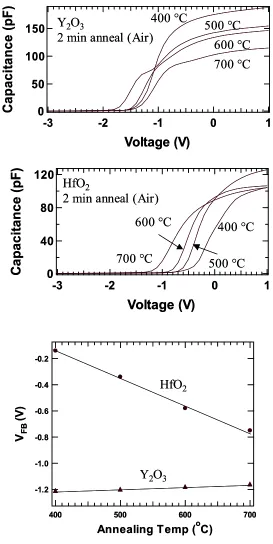
FIGURE 4.1: XPS OF PVD Y AND AL METALS... 60
FIGURE 4.2: XPS OF PVD HF AND AL METALS. ... 61
FIGURE 4.3: EFFECTS OF TEMPERATURE ON FLATBAND VOLTAGE FOR END MEMBER Y2O3 AND HFO2 FILMS... 62
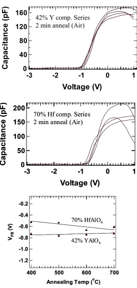
FIGURE 4.4: EFFECTS OF TEMPERATURE ON FLATBAND VOLTAGE FOR 42% Y2O3 AND 70% HFO2 FILMS... 63
FIGURE 4.5: HYSTERESIS FOR 42% YALOX FILM WITH FLATBAND VOLTAGE, VFB. ... 64
FIGURE 4.6: HYSTERESIS FOR 70% HFALOX FILM WITH FLATBAND VOLTAGE, VFB. ... 65
FIGURE 4.7: EFFECTS OF AL ALLOYING ON YTTRIUM AND HAFNIUM FILMS. ... 66
FIGURE 4.8: THE EFFECT OF ALUMINUM ALLOYING ON EQUIVALENT OXIDE THICKNESS (EOT) FOR YALOX FILMS. ... 67
FIGURE 4.9: THE EFFECT OF ALUMINUM ALLOYING ON EQUIVALENT OXIDE THICKNESS (EOT) FOR HFALOX FILMS... 68
FIGURE 5.1: SCHEMATIC DRAWING OF PECVD REACTOR... 82
FIGURE 5.2: SCHEMATIC DRAWING OF ALD REACTOR... 83
FIGURE 5.3: SCHEMATIC DRAWING OF PVD REACTOR... 84
FIGURE 5.4: AUGER ANALYSIS OF RUO2 ON HFO2... 85
FIGURE 5.5: XPS ANALYSIS OF HF 4F PEAK FOR RUO2 ON HFO2... 86
FIGURE 5.6: CV CHARACTERIZATION OF RUO2 ON SIO2... 87
FIGURE 5.7: CV CHARACTERIZATION OF RUO2 ON HFO2. ... 88
FIGURE 5.8: CV COMPARISON OF EX-SITU VERSUS IN-SITURUO2 ON HFO2 PROCESS. ... 89
FIGURE 6.1: CAPACITANCE VS. VOLTAGE MEASUREMENTS FOR 0.8NM HF-METAL FILMS OXIDIZED IN N2O (FIG. 6.1A) AND N2(FIG. 6.1B) WITH AL GATES AS A FUNCTION OF OXIDATION TIME (LEGEND). OXIDATION IN N2O FOR 300S RESULTS IN SUBSTANTIAL REDUCTION OF THE CAPACITANCE AND GENERATION OF POSITIVE FIXED CHARGE IN THE FILMS. OXIDATION UP TO 300S IN N2 DOES NOT HAVE A SIGNIFICANT EFFECT IN THE ELECTRICAL PROPERTIES OF THE FILMS... 105
FIGURE 6.2: EQUIVALENT OXIDE THICKNESS (EOT) AND FLATBAND VOLTAGE VFB VS. OXIDATION TIME FOR 0.8NM HF-METAL FILMS OXIDIZED IN N2(SQUARES) AND N2O
(CIRCLES). OXIDATION OF HF-METAL ON SI IN N2O LEADS TO GROWTH OF THICK
FIGURE 6.3: EQUIVALENT OXIDE THICKNESS (EOT) AND FLATBAND VOLTAGE VFB VS.
OXIDATION TEMPERATURE FOR 2.5NM HF-METAL FILMS OXIDIZED IN DRY AIR FROM 2 MIN IN AN RTA. OXIDATION OF HF-METAL ON SI AT HIGHER TEMPERATURES LEADS TO
GROWTH OF THICK INTERFACIAL LAYERS THAT IS ACCOMPANIED BY THE GENERATION OF LARGE AMOUNTS OF CHARGE AS EVIDENCED BY THE SHIFT IN VFB. ... 107
FIGURE 6.4: SHIFT IN THE VFB AS A FUNCTION OF THE INTERFACIAL LAYER THICKNESS INCREASE. FOR THE SAMPLES OXIDIZED IN THE RTA (DIAMONDS) THE VFB AND EOT OBTAINED FOR THE 400°C OXIDATION IS TREATED AS THE BASELINE MEASUREMENT. FOR THE SAMPLES OXIDIZED IN THE TUBE FURNACE IN N2O AT 600°C (CIRCLES) THE VFB AND
EOT OBTAINED FOR THE 90S OXIDATION IS TREATED AS THE BASELINE MEASUREMENT.
... 108 FIGURE 6.5: HF 4F, SI 2P AND O 1S SPECTRA FOR 0.8NM-METAL FILMS OXIDIZED IN (I) N2O FOR
30S (II) N2O FOR 90S (III) N2O FOR 300S AND (IV) N2 FOR 300S. SPECTRA (I), (II) AND (IV) ARE PRACTICALLY IDENTICAL AND CORRESPOND TO SAMPLES WITH COMPARABLE
ELECTRICAL PROPERTIES. WE CAN OBSERVE THE GROWTH OF THE SIO2 PEAK IN THE SI 2P SPECTRUM FOR SAMPLE (III), RESULT OF THE FAST INTERFACE OXIDATION ACHIEVED IN
N2O. ... 109 FIGURE 7.1: SCHEMATIC DRAWING OF ALD REACTOR... 122
FIGURE 7.2. AES OF C KLL PEAK AND O KLL PEAK OF HFO2 AT INITIAL CONDITION AND AFTER A 325°C THERMAL TREATMENT FOR 40 MINUTES. ... 123
FIGURE 7.3. AES SURVEY SPECTRA OF ALD RU GROWTH SERIES... 124
FIGURE 7.4. THE C KLL PEAK AND O KLL PEAK OF ALD RU FILMS AT AFTER O2 PULSE AND
RU(CP)2 PULSE DURING THE ALD PROCESS... 125
FIGURE 7.5. AES SPECTRA OF ALD RU FILMS AT 380°C ... 126
FIGURE 7.6. ATOMIC PERCENT COMPOSITION OF RU FILM SURFACE DURING EACH STEP OF THE
Chapter 1 Introduction
Historical Perspective
In 1947, the invention of the metal-oxide-semiconductor field-effect transistor (MOSFET) by Bardeen, Brattain, and Shockley [1] and the subsequent development of
monolithic silicon based integrated circuit fabrication techniques has led to unprecedented levels of growth in the semiconductor industry through the latter half of the 20th century. The scaling of silicon based microelectronic devices and integrated circuits were originally
predicted by Gordon Moore [2] in 1965 to last at least a decade. Through the years, complementary metal-oxide-semiconductor field-effect transistor (CMOSFET) device
scaling to ever smaller physical dimensions has led to continuous improvement in microelectronic device performance and to its widespread proliferation which now constitute about 90% of the semiconductor device market. Phenomenal advances in photolithography
techniques, tools and pattern transfer processes and equipment have however, ensured the validity of Moore’s Law well into the 21st century. In an evolution driven primarily by
photolithography, minimum feature sizes on devices have been scaled down from several microns in the 1970’s to less than 100nm today. This has enabled consistent improvement in device packing densities on chips, enhancement in circuit speeds and vastly improved
performance-to-cost ratios for microelectronics based products. As a result of aggressively scaled devices, scientist and engineers will have to address the rapidly approaching physical
process integration engineers and materials scientists alike and the need for enhanced cross-disciplinary research has seldom been more promising.
Complementary metal oxide semiconductor
Complementary metal oxide semiconductor (CMOS) transistor technology has traditionally relied on Si (element or as part of a compound) in several morphological forms
(bulk single crystalline, thin film polycrystalline, thin film epitaxial) to serve the varied functions that are needed for the satisfactory operation of a field-effect transistor. Silicon and Si based materials have thus been used in several functional forms as semiconductor
(channel, body), insulator (gate dielectric, inter-metal dielectric) and conductor (gate electrode, silicide contacts) in a conventional field-effect transistor, shown in figure 1.1.
While thermodynamically stable, ease of formation and acceptable dielectric properties have been some of the motivations behind the use of SiO2 as a gate dielectric; ease of process integration and device performance issues like threshold voltage control have been the
important considerations in the use of poly-silicon gate electrodes. Research over the last few years indicates an increasing use of metal-based stack materials for future CMOS devices [3].
In order to be acceptable for use as gate electrodes in future CMOS devices, candidate materials must posses several general physical properties and must lend themselves
easily to conventional Si processing techniques (lithography, deposition (physical/chemical vapor), etching (dry/wet), etc.). Candidate metals must have high (> 1000 ºC) melting points and must be thermodynamically stable on the MOSFET gate dielectric (SiO2 or other
after rapid thermal processing). In addition to these requirements, the selection of materials for this application is also constrained by the need to obtain low and symmetric threshold voltages on the N- and PMOSFET devices. The gate electrode of a MOSFET influences the
threshold voltage of the transistor through its work function. In order to obtain low and symmetric threshold voltages on the two types of devices, while maintaining acceptable short
channel performance, it is essential that the two gate electrodes have different work functions. The ideal gate work function for bulk-Si NMOSFETs (PMOSFETs) is ± 0.2V of the EC (EV) of Si respectively [4] (shown in figure 1.2). It is thus evident that the integration
of multiple metals on a single substrate or the development of a single metal tunable work function schemes will become necessary in future CMOS gate stacks. From a process
perspective, the latter is highly desirable. Engineering the work function of a metal thin film at dielectric interfaces is however not trivial. This dissertation will briefly discuss different approaches developed to fabricating dual-metal gate CMOS devices and focus on a novel
single-metal tunable work function approach that might assist in the integration of metal gates into CMOSFET devices.
Objective of this work
Our primary objective is to investigate alternative candidate materials for the replacement of Si-based gate stack materials specifically replacing current SiO2 dielectrics
and poly-Si gates. Since it will be crucial to replace these materials simultaneously, our goal throughout this dissertation is to holistically research candidate materials in tandem. The primary goal was to develop optimal deposition processes for both dielectrics and gate
properties leading candidate materials and the effects they have at the interface. The third goal was to understand the chemical reactions that take place during the deposition processes.
Overview of Dissertation
This dissertation has been focused on understanding process reaction mechanisms during processing of candidate alternative gate stack materials for CMOSFET applications.
The impact these materials will have for future CMOS devices were evaluated. For dielectrics, the flatband voltage was tunable with alloying Al2O3 with Y2O3 or HfO2 with yttrium aluminates being most sensitive to small changes in atomic percentages of Al
incorporation. Also, the film composition for ruthenium films grown by atomic layer deposition varies between reactant pulse with an adsorbed oxygen layer after the oxygen
pulse which later reacts with the precursor ligands.
Chapter 2 illustrates the guidelines necessary for selecting alternative gate stacks materials and highlights some of the challenges for their succession to current Si-based
materials. Interfaces stabilities when in contact with other materials (specifically thermal stabilities of dielectrics in contact with the silicon substrate and gate electrodes in contact with the dielectric) are also highlighted.
Chapter 3 discussed the possible techniques used to fabricate alternative gate stack materials. The choice of processing technique used to fabricate the materials must allow for
easy implementation into current CMOS processing technologies. Also, the methods for analysis the materials are discussed which include techniques for physical, chemical, and electrical characterization.
silicon. Successful flatband voltage tuning is present and the yttrium alluminate films were most sensitive to small changed in Al composition. Capacitance versus voltage analysis indicates that the addition of Al to Hf and Y oxides results in a positive shift in flatband
voltage with increasing Al concentration for both set of mixtures. Also, the suppression of interfacial layer formation was significantly reduce with small amounts (<5 atomic percent)
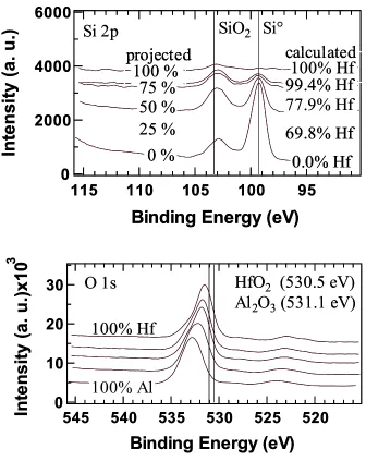
of Al which is indicated by reduction of equivalent oxide thickness (eot) values. X-ray photoelectron spectroscopy (XPS) investigation of Y(or Hf) and Al chemical states of the alloy films indicate the films are a homogenous mixture of HfO2 (or Y2O3) and Al2O3.
Chapter 5 we evaluate ruthenium-based metals as potential candidates for gate electrodes in advanced gate stack applications. We deposited RuO2 metal from
tris-tetramethyl-heptadianato Ru (Ru TMHD) introduced downstream from a remote N2O plasma at 365 and 500°C, and examined the deposited film and interface structure using Auger and X-ray photoelectron spectroscopies. The films show some evidence for N and C
incorporation, consistent with the 250°C decomposition temperature of the Ru TMHD. Based on AES results, the O/Ru ratio is larger for the films deposited at higher temperature. Because of the difference between the oxidizing and reducing environments in CVD
processing, we expect that metallic oxides such as RuO2 will result in different metal/dielectric interface structure than for elemental metal/dielectric interfaces. To examine
the role of deposition chemistry on interface structure, several thicknesses of RuO2 have been deposited by plasma CVD on HfO2 formed in our lab by atomic layer deposition. The effect of HfO2 surface structure, and the trends in RuO2 composition with film thickness
Chapter 6 describes how the oxidation of Hf metal films on Si appears to follow different charge generation rules than the traditional oxidation of Si described in detail by Deal et al. Oxidation of thin Hf metal films on silicon in oxygen rich environments to form
Hf-silicate results in rapid growth of silicon oxide interfacial layers and generation of significant charge concentration in the films. Oxidation of Hf in oxygen-deficient
environment leads to improved control of the interface with much thinner interfacial layers and substantial reduction in the charge present in the films. Results from capacitance vs. voltage and x-ray photoelectron spectroscopy measurements are compared to correlate
charge with chemical structure evolution during oxidation and dielectric layer formation. It is demonstrated that processing conditions may influence the quality of the Hf dielectric film
significantly by generating positive charge that is not intrinsic to the material.
Chapter 7 evaluates the role of atomic layer deposition (ALD) ruthenium films from bis(cyclopentadienyl) ruthenium (RuCp)2 using online Auger Electron Spectroscopy (AES)
to identify surface composition of the films during the ALD process. The AES results show significant changes in film composition when comparing the surface after the precursor pulse and the reactant pulse. The compositions show evidence that the ruthenium films form an
References
1. Shockley, W., The Path to the Conception of the Junction Transistor. Ieee Transactions on Electron Devices, 1984. 31(11): p. 1523-1546.
2. Moore, G.E., Cramming More Components onto Integrated Circuits. Electronics, 1965. 38(8).
3. Wong, H.S.P., Beyond the conventional transistor. Ibm Journal of Research and Development, 2002. 46(2-3): p. 133-168.
Figure 1.1: Illustration of a complete CMOS structure
P-sub
P+ N P+ N+ P N+
N well P well
Channel
Gate electrode
Gate dielectric S/D extensions
P-sub
P+ N P+ N+ P N+
N well P well
P-sub
P+ N P+ N+ P N+
N well P well
Channel
Gate electrode
Figure 1.2: Comparison of metal workfunctions for midgap metal and dual metals. PMOS VT
NMOS VT
TiN Pt Al
Vacuum Level
Single Midgap Metal Dual Metals
Si EC EC
EV EV
1.1 eV
b
a
Ф
MФ
MФ
MPMOS VT NMOS VT
TiN Pt Al
Vacuum Level
Single Midgap Metal Dual Metals
Si EC EC
EV EV
1.1 eV
b
a
Chapter 2 Metal Gate CMOS Technology
Advanced Gate Electrode Materials
Polycrystalline silicon (poly-Si) has been used as a MOSFET gate material for several
decades. One of the primary reasons for this is its high compatibility with CMOS processing. Poly-Si can be very easily deposited by low-pressure chemical vapor deposition (LPCVD) techniques and it displays excellent thermal stability on SiO2, which has been the
gate dielectric of choice for MOSFETs. From a device performance perspective, the most important property of the gate electrode is its work function at the dielectric interface. In a
MOS system, it is the work function of the gate that controls the threshold voltage of the device, by controlling how much applied voltage is necessary to bring about inversion in the transistor substrate. For a CMOS technology, it is generally desirable to have low and
symmetric threshold voltages on the N- and PMOS devices. As device channel lengths have been scaled down over successive technology generations, dopant concentrations in the
channel have been increased in order to maintain good short channel performance (i.e., in order to prevent the channel depletion region from becoming too large and the drain depletion charge from significantly penetrating into the channel region). This in turn requires
the gate work function to be close to EC and EV for bulk-Si N- and PMOS devices respectively (so that reasonably low threshold voltages can be maintained). Adjusting the
dopant concentrations in the transistor channel can also control the device threshold voltage. In principle, a single gate material with Fermi level near the middle of the Si bandgap could be used for both N and PMOS operation, it would not allow the threshold voltages to be kept
integration benefit comes from the ease with which an undoped poly-Si can be converted to a low work function (n+) or a high work function (p+) film using ion implantation of appropriate dopants (donors or acceptors) followed by thermal annealing.
Perhaps the most pressing reason to look at alterative gate materials for deep-submicron CMOS devices arises from the fact that a heavily doped poly-Si gate will become
depleted at the gate/dielectric interface when the channel is in inversion[1]. A schematic band diagram across the MOS stack is shown in Fig. 2.1 to illustrate this phenomenon.
A depletion layer in the gate can be harmful in several ways. It adds a capacitance in
series to the gate dielectric capacitance and thus adds to the effective dielectric thickness between the gate and the channel. This implies a reduction in the capacitive coupling
between the gate and the channel in inversion. For comparable channel currents, the reduction in the inversion capacitance in the case of a poly-Si gate device lowers the drive current significantly [2]. The gate depletion effect is of particular concern for
deep-submicron CMOS technology. As the dielectric thickness is scaled to 1nm and below in sub-50nm devices [3, 4], even the addition of a few tenths of a nanometer in the form of a depletion layer can significantly increase the effective dielectric thickness of the device. This
would also be a serious setback to all efforts to scale down the gate dielectric thickness using high-permittivity gate dielectrics. Because of this, many researchers have investigated
alternative gate electrode materials, which can either reduce or eliminate the gate depletion effect. The use of metal gate materials is most beneficial for devices with very thin EOT (< 1nm) where high performance (high drive currents) is most important. While refractory
integration challenges that must be overcome before a viable metal-gate CMOS technology can be developed.
In addition to the gate depletion effect, thermodynamic incompatibility with high-k
gate dielectric is also an issue for poly-Si gate technology. There have been successful demonstrations of MOS capacitors and transistors with ultra-thin EOT using high-k gate
dielectrics viz. oxides of Hf, Zr, Al, Y, and La [5-9]. Many of these materials are not thermally stable in contact with poly-Si above certain temperatures, and therefore cannot be used in a conventional dual poly-Si gate CMOS process, in which the highest activation
annealing temperature can exceed 1000ºC. Therefore, alternative gate materials that are thermally stable with various advances gate dielectric materials will be needed. It must be
mentioned however, that the high-k dielectric is typically separated from the Si substrate by a thin interfacial layer (SiO2, Si3N4, or an oxy-nitride) and hence the bottom interface can withstand elevated temperatures.
When ultra-thin gate dielectrics are used in conjunction with poly-Si gate electrodes, dopant penetration from the gate into the channel can be a significant problem. It has been especially severe for p+ gate electrodes given the small mass and high diffusivity of B in Si.
Boron penetration has also been observed to occur through high-k dielectrics [10] and is a potentially significant concern for future gate stacks since it leads to instabilities in device
operations.
An additional concern with poly-Si gate electrodes is the active dopant concentration limited conductivity. For CMOS applications, the poly-Si gate electrode is deposited
physical dose of dopant ions implanted into the gate, the thermal budget allowed to activate the dopants (ie. move them to substitutional sites in the Si lattice) and the solid solubility of the dopant atoms in Si. This might lead to unreasonably high resistivities on the gate lines.
For example, when dopants are implanted in the poly-Si gate, they need to be “activated” by
a high-temperature anneal (up to 1100°C) to diffuse the dopant atoms to lattice sites and
make them electrically active (thereby making the gate conductive). However, current
CMOS processes use lower temperature anneals (~950°C) to limit unwanted dopant diffusion
in other regions of the device. Therefore, the poly-Si is not completely activated and has some finite capacitance, because it is not completely conductive. In operation, this
poly-depletion effect adds a series capacitance with an EOT of 3-7Å to the gate stack, which becomes a significant problem as industry attempts to scale the gate stack to EOT values below 10nm. A further difficulty arises with the continued scaling of the physical
dimensions of the gate electrode. According to the International Technology Roadmap for Semiconductors (ITRS) [11], the aspect ratio for the gate electrode is expected to remain
constant (height/length) as the gate length is scaled down. Concomitantly, the gate sheet
resistance is to be maintained at 5 Ω/ . This implies the need for a steady increase in gate
active dopant concentrations as the gate length is scaled down. If the use of high-k gate dielectrics precludes the use of high thermal budgets for dopant activation, it is unclear how
the specified values of active dopant concentration and gate sheet resistance would be achieved in a poly-Si gate technology. The solid solubility of the commonly used dopants in
Si poses physical limitations on the gate sheet resistance. In order to achieve required gate
sheet resistance of 5 Ω/ , the active dopant concentration in the gate would have to be
are ~1x1020 cm-3, 2x1020 cm-3, and 3x1020 cm-3 respectively [12]. It should be noted that the required active dopant levels would imply super-saturated solutions of B in Si and near 100% activation of P and As.
Metal gate materials thus appear to be very attractive candidates for future CMOS devices. However, there are significant process integration challenges that must be overcome
before a metal gate technology can be considered to be viable for integrated circuit manufacturing.
Selection of Materials
Candidate gate materials must satisfy several criteria in order to be viable for use in a Si-based CMOS fabrication process. As mentioned earlier, for sub-65nm technology nodes,
the ITRS specifies a gate sheet resistance of ≤ 5 Ω/ . Thus these materials must be highly
conductive and must have very high melting points, and be stable in contact with the high-k dielectric in order to withstand thermal budgets commonly used in CMOS processing. It is also important that these materials lend themselves easily to conventional thin-film
deposition (physical or chemical vapor) and reactive ion etching (RIE) techniques. These requirements will ensure that advanced gate CMOS devices can still be fabricated using
conventional tools. The new gate materials also need to have thermal expansion coefficients that closely match those of the single crystalline Si substrate in order to ensure that no significant thermal stresses are introduced in the film during rapid temperature changes (as
used for dopant activation), and they must have good adhesion with the underlying dielectric. The general requirements described above already limit the candidate materials to some of
The most significant constraint in the choice of gate material, however, relates to the need to precisely engineer the transistor threshold voltage. As mentioned earlier, in order to obtain low and symmetric N- and PMOSFET threshold voltages (VT) while suppressing
short-channel effects, it is essential to have the gate work function between ± 0.2eV of EC and EV for bulk-Si N- and PMOSFETs respectively [3]. There is thus a need to identify
metallic materials that have work functions close to the above value and to develop process integration schemes that will provide multiple gate work functions for NMOS and PMOS devices integrated on a single Si substrate. A further challenge is imposed by the dependence
of the metal work function on the properties of the underlying dielectric film. In general, metal work functions at dielectric interfaces differ from their values in vacuum [13]. This
observation and its theoretical origins indicate that the search for metal gate materials must be conducted in tandem with the search for alternative gate dielectrics. It should also be noted that metals with complementary work functions also display inherent differences in
physical properties like reactivity. Low work function metals are typically easily oxidized while high work function metals are inherently inert. This imposes additional constraints on the choice of metal gate material and process integration schemes.
Candidate Materials
The choice of materials are governed by two sets of requirements alluded to earlier in
Physical Properties
Candidate gate metals need to be thermodynamically stable on the gate dielectric and must be able to withstand thermal budgets commonly used in CMOS fabrication. The
highest temperatures used in device fabrication are for the activation of dopant atoms in the source, drain, and gate regions of the transistor. Typical activation thermal budgets include
rapid thermal annealing at temperatures just above 1000ºC (either a spike anneal with no soak time or for a few seconds soak at the highest temperature). This implies minimum melting temperature of well above 1000ºC for assured thermal stability. While nitrided SiO2
is the currently used dielectric, it would be very likely that a change from SiO2 to higher permittivity dielectrics will occur simultaneously with that from poly-Si to alternative gate
electrode materials. Hence, the new gate electrode material must be chosen in tandem with potential high-k materials being explored. The choice of high-k gate dielectrics is governed by similar thermal stability concerns with the Si substrate and specific physical and
electronic properties such as the permittivity, band gap, electron and hole effective masses and band offsets with respect to the Si substrate. A modest permittivity (k~20-30) is expected to be an optimum value given the inverse relationship between permittivity and
band gap (a smaller band gap is undesirable as it would lower the barrier height for electron or hole tunneling between the gate and the channel). Over the last several years, many
research groups have actively pursued the search for new gate dielectrics starting from purely theoretical thermodynamic considerations [14] to experimental demonstrations of high-k MOS capacitors and transistors [15-17]. While a lot of work remains to be done in this field,
gate dielectrics. It is essential that the thermal stability of alternative gate materials on at least a subset of candidate dielectrics be experimentally verified. Typically, low work function metals are fairly reactive (prone to oxidation) (eg. Al, Ti, Ta) while high work
function metals tend to be inert (eg. Ni, Pt, Pd, etc.) and naturally immune to oxidation. The techniques used to deposit the gate electrode affects a number of important
properties of the gate electrode. The morphology of the gate electrode is important for several reasons. An amorphous gate electrode is likely to have a work function significantly different from that of a crystalline one. In addition, different crystalline facets of a single
crystal typically display a wide range of work functions. Thus, it is critical to identify deposition conditions that will lead to appropriate film morphologies and orientations.
Furthermore, the deposition technique will also affect the quality of the interface between the gate electrode and the dielectric. In general, a deposition technique that permits sharp interfaces to be obtained is desirable. Most metal thin films are deposited using physical
vapor deposition (PVD) techniques viz. sputtering (using DC, magnetron, or RF sources) or evaporation (using electron beam or thermal evaporation). Unfortunately, most of these techniques involve the use of energetic particles (ions, electrons) and are mostly likely to
impart physical damage to the gate dielectric (rough interfaces, metal ions penetrating into the dielectric, etc.) and result in degraded gate dielectric reliability [18, 19]. Chemical vapor
deposition techniques would lead to minimal damage to the underlying dielectric and are desirable for this application. Chemical vapor deposition will also provide a number of variables, viz. temperature, pressure, gas flow to control the film microstructure. However,
very well identified or characterized. This is a challenging area that can be expected to become even more important as CMOS technology continues to be scaled down.
Yet another important consideration in the choice of a gate material is its
patternability. Gate films will need to be etched with high selectivity to the underlying dielectric. In addition, the gate etch should ideally result in vertical sidewalls without any
protrusions or notches at the dielectric interface. This implies optimizations of reactive ion etch chemistries and process conditions that ensure high etch selectivity and ideal sidewall profiles. While wet etch chemistries might also be used to remove metal films with high
selectivity to the gate dielectric, the use of wet etchants for sub-50 nm line patterning is unlikely given the isotropic nature of wet etching processes. The choice of gate material will
have to account for the inherent reactivity or inertness of the metal under consideration. State of the art CMOS fabrication processes involve the use of rapid thermal annealing (RTA) to activate dopant atoms in the source, drain, and gate with minimal
diffusion. Typical RTA temperatures are between 900-1000ºC and typical annealing times range from a few seconds to a minute. In some cases, spike annealing (no soak at peak temperature) is also used. Temperature ramp-up is typically between 200-250ºC/s and
cool-down of the wafer is also very rapid. This rapid thermal cycling can become a source of thermally induced stresses in the MOS stack and might lead to cracking or peeling of gate
Work Function
The most direct impact of the gate electrode on the operation of a MOSFET is through its control of the device threshold voltage (VT). The voltage required for the onset of
inversion in the MOSFET channel is determined by the work function of the gate electrode. The threshold voltage of a MOSFET is typically given by the following expression:
OX B a Si FB T C qN V
V = + 2ε 2φ
where ε is the permittivity of Si, q is the electronic charge, Na is the dopant concentration in
the channel, φB is the band bending in the Si substrate and Cox is the oxide capacitance. VFB
is the flat band voltage across the MOS stack and denotes the voltage applied on the gate electrode that eliminates any band bending across the stack. VFB is given by the following expression: OX f B MS FB C Q V =Φ +2φ ±
where ΦMS indicates the work function difference between the metal gate and the Si substrate and Qf denotes the magnitude of fixed charge in the oxide film.
The gate electrode through the work function difference between the gate and the
channel thus directly controls the threshold voltage of the MOSFET. The band bending in the channel is given by the following expression:
= i a B n N q kT ln φ
where ni is the intrinsic Si carrier concentration. For typical channel doping levels used
implies gate work function values of ~ 4.1V for NMOS and ~ 5.1V for PMOS devices. More precise calculations performed using 2D device simulations [3] indicate that for an optimum combination of short channel performance and device drive current, gate work functions for
sub-50 nm bulk CMOS transistors should be between ± 0.2eV of EC (EV) for NMOS (PMOS). Sub-100 nm gate length bulk-Si MOSFETs typically need fairly high dopant
concentrations in the channel regions to prevent the drain depletion region from penetrating excessively into the channel leading to poor short-channel performance. However, high levels of channel doping typically degrade carrier mobility in the transistor channel.
Metal Gate/High-k Dielectric Integration
An important consideration in the selection of metal gate electrodes is the work
function dependence in contact with high-k dielectric. In general, the work function of a metal at a dielectric interface is different from its value in vacuum. This variation needs to be taken into account when designing transistor gate stacks with alternative gate dielectrics.
The dependence of the metal work function on the permittivity of the gate dielectric has been explained by Lu et al [20] using experimental data in conjunction with interface dipole theory [21]. In order to accurately predict metal work functions at dielectric
interfaces, one needs to take into account charge transfer across such interfaces. In general, there are always intrinsic interface states at metal-dielectric interfaces [22] which can be
predominantly donor like (closer to EV) or acceptor like (closer to EC). When an interface is formed between a metal and a dielectric, these interface states can get charged up resulting in a dipole that will drive the bands to align in a way that minimizes the charge transfer. The
the metal Fermi level (EF,M) is above the dielectric charge neutrality level (ECNL,D), the dipole layer created at the interface will be charged negatively on the dielectric side. This dipole will tend to drive the metal Fermi level towards ECNL,D and hence the effective metal work
function (ΦM,eff) will be different from the vacuum metal work function (ΦM,vac). This work function change is proportional to the difference between ECNL,D and EF,M, or equivalently,
the difference between ΦM,vac and ΦCNL,D. Taking into account the effects of charge screening in the dielectric, the effective metal work function ΦM,eff is given by
(
Mvac CNLD)
D CNL eff
M, =Φ , +S Φ , −Φ ,
Φ
where S is a slope parameter that accounts for dielectric screening and depends on the
electronic component of the dielectric constant, ε∞, [23] according to
(
)
[
2]
11 1 . 0
1+ ∞ − −
= ε
S
A larger dielectric screening lowers the slope parameter S and increases the degree of pinning
of the metal work function to ECNL,D. Values for ε∞ for various dielectrics of interest (SiO2,
Si3N4, HfO2, and ZrO2) have been used to calculate the slope parameters for these dielectrics.
Comparison of theoretical and measured interfacial work functions for several metals of interest (Al, Ti, W, Mo, and Pt) led to reasonable agreement indicating the validity of the theory. An important conclusion of this work was highlighted in [20], where it was shown
that in order to obtain ΦM,eff of 4.05V (5.17V) for NMOS (PMOS) gate electrodes, metals with even smaller (larger) ΦM,vac have to be used as the permittivity of the gate dielectric is
integration since very inert metals are by definition difficult to etch (a general lack of volatile compounds) while reactive metals are likely to react with the underlying gate dielectric (typically an oxidation reaction where oxygen from the dielectric can preferentially bond
with the gate metal).
Process Integration
In general, one may use a combination of two or more metals on a single Si substrate to achieve the work function requirements discussed above. While the processes described herein have been successfully implemented, it must be noted that the integration of multiple
metals on a single wafer poses significant process integration challenges and it would be highly desirable to develop a single metal tunable work function gate CMOS process. Such a
process would allow for minimal process complexity and would be relatively easy to integrate on a single Si substrate.
Dual Metal Gate CMOS Technology
Probably the most intuitive approach to developing a metal gate CMOS process involves the use of two metal, on serving as the NMOS gate and the other as the PMOS gate. Process integration is however not very straightforward since two film deposition steps and
at least two etch steps would be involved.
The general process involves the deposition of one metal over the entire substrate
after active area definition and gate dielectric deposition. Following the first deposition, a well lithography is performed to expose either n- or p-well regions and the exposed metal is removed using a wet etch chemistry. For example, if the first metal is appropriate for NMOS
removal of the two metals and the selectivity of the etch chemistries on the gate dielectric. Following the removal of the first metal, the photoresist is stripped and after rinsing the wafer, a second metal is deposited over the substance. In doing so, a bilayer metal stack is
formed on one half of the substrate, while a single layer gate is formed over the other half and each well has a different metal in direct contact with the gate dielectric. In order to
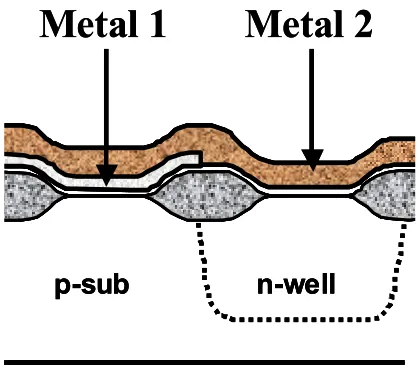
prevent interdiffusion between the two metals on the side where a bilayer is formed, a thin diffusion barrier metal (< 5nm) can be deposited over the first metal before patterning. Figure. 2.2 shows a schematic cross-section through the gate stacks after the two deposition
steps. Following the second deposition, photolithography is used to define the gate lines on the N- and PMOS sides.
One concern arises from the fact that the first gate metal is chemically removed over the gate dielectric on one of the wells. In doing so, it is likely that the chemicals used for the metal etch can also attack the thin gate dielectric film. This was also observed in the case of
the Mo and Ti gate process where the Ti etchant also attacked the Si3N4 gate dielectric on the n-well. This discrepancy is generally intolerable, as it would lead to substantial mismatch in the performance of the two types of devices. If a different combination of gate metals and
dielectric is used, it might be possible to avoid this drawback, however, any exposure of the dielectric to metal etchants is likely to affect the long term reliability of the gate dielectric
film and should be avoided as much as possible. Hence, it is unlikely that the process mentioned herein can be ported to manufacturing as described. One solution is to intentionally remove the gate dielectric entirely over the n-well (or p-well) after removing the
solution can provide for a more reliable gate dielectric film, it introduces substantial process complexity (removal of dielectric film over first metal film on one well).
Gate lithography of the asymmetrical gate stack presents another concern since the
optimal focus depths for the two wells can be substantially different. Another concern lies with developing a high selectivity reactive ion etch process for the asymmetrical gate stacks
on the n- and p-wells. Since one well will have a bilayer metal stack and the other well will have only a single metal layer, a high etch selectivity is needed between the second gate metal and the gate dielectric.
Metal Interdiffuion Gate CMOS Technology
A technique that alleviates some of the above mentioned concerns was developed
[23] and referred to as metal-interdiffusion-gate (MIG) CMOS process since it relies on interdiffusion between two (or more) metal films. This approach can be implemented as follows.
Following gate dielectric deposition, a first metal layer is deposited and immediately capped with a second metal layer. The first metal film is intentionally kept thin (≤ 10nm) while the second metal film can be much thicker. In the next step, resist lithography is used
to expose and remove the top metal film over one of the two wells. For example, if the first metal has a work function corresponding to that for NMOS devices, then the second metal is
removed over the those areas (p-wells) and vice-versa. Following selective removal of the second metal, gate lithography can be preformed to define gate lines on both the wells. After gate definition, an interdiffusion anneal is performed to interdiffuse the two metals in the
If the metals do not thermodynamically prefer to alloy over the temperature range used and simple prefer to intermix, the resulting bilayer gate will have a work function that corresponds to that of the mixture. The exact value is however difficult to predict and will
depend on the extent of the intermixing (which in turn depends on the relative thicknesses of the two metals films, the interdiffusion coefficients, etc.)
Another outcome can lead to the diffusion of the top metal through the bottom layer and its segregation at the dielectric interface. This will lead to the threshold voltage of the resulting transistor being determined entirely by the segregated metal layer. In effect, the
bottom layer can act as a sieve to allow the top metal to pass through. This approach was demonstrated with the use of Ni and Ti bilayer gate stacks [23] and was shown to lead to low
and symmetrical threshold voltage n- and p-channel transistors. Ni and Ti were chosen for this demonstration since they have complementary work functions (~ 5V and ~ 4V respectively). Ni was used at the top metal. Ni is a fast diffuser in Ti [24, 25] and is also
known to segregate at the SiO2 interface. Even at the relatively low temperature used for interdiffusion (400ºC), x-ray photoelectron spectroscopy (XPS) results indicated that interdiffusion was complete and elemental Ni was observed at the SiO2 interface. This
indicates that Ni is stable on SiO2 up to 400ºC and does not preferentially form metal silicides or oxides.
Another possible outcome is the preferential alloying of the two metals to form a binary alloy with a work function determined be the exact composition of the alloy. This approach was recently demonstrated using Ru-Ta system [26]. Co-sputtering of several alloy
potentially be applied to that system as well [27-29]. It is thus important to note that the general MIG concept can also be extended to ternary systems.
The primary advantage of a MIG approach over the dual-metal gate approach
described earlier lies in the protection of the gate dielectric at all times since the bottom metal layer is always present to protect the dielectric. Hence, reliability problems associated with
the earlier approach can be prevented.
Work Function Engineering
The work function of a metal depends on several physical and chemical properties.
The conventional definition of the work function of a metal quantifies it in terms of the energy required to remove an electron from the metal surface [30]. Implicit in this definition
is the idea that the energy required to remove an electron from a metal is primarily a property of the surface and specifically a property of the interface between the metal and its surrounding medium. From a purely thermodynamic perspective, the work function of a
metal can also be defined in terms of the chemical potential within the metal (the Fermi level is in fact one manifestation of the Gibbs free energy of a metal). From a thermodynamic perspective then, structural and/or chemical changes at a metal surface are likely to change
the free energy at that surface and hence affect the work function. The notion that structural or chemical changes in a thin metal film are likely to affect its work function is one of the
primary hypotheses of this work. This section will discuss various approaches developed to modulate thin film work functions and the feasibility of some of these approaches.
Structural Modification
modification (disruption) in the long-range order within the crystal lattice. In general, metals display anisotropy in their work function [13]. The origin of this anisotropy is believed to be the difference in atomic packing density along the various crystallographic planes. Densely
packed crystallographic surfaces display high work functions since these surfaces are smooth and relatively inert with fewer broken atomic bonds (most bonds are within the plane). Open
crystallographic surfaces display lower work functions owing to a greater number of broken bonds (larger fraction of bonds outside the plane). Smoluchowski [31] has developed a formal semi-quantitative theory to explain this anisotropy based on a similar crystallographic
analysis. Amorphous metal films are expected to have lower work functions than their crystalline counterparts.
Chemical Modification
There are several ways to selectively change the chemistry of thin metal films deposited on high-k substrates. It should be noted however, that the final chemistry of the
film should be such that the film retains near metallic conductivity. As such, conducting metal nitrides, metal silicides and conducting metal oxides are potential candidates. This section describes a few techniques developed to implement this approach.
A very powerful yet straightforward way to introduce foreign elements into a film is ion implantation. Ion implantation is an attractive approach for a number of reasons. If the
work function can indeed be modulated over the desired range, ion implantation can provide for a highly integrable and CMOS compatible process since photoresist masking can be used to selectively implant the desired ions. In addition, ion implantation is a technique that has
possible). In addition, fairly sophisticated simulators are available to model implanted depth profiles in a variety of substrates with fairly high precision.
An alternative way to introduce nitrogen into metal films is to use a sacrificial layer
as a solid diffusion source. In this approach, thin metal films (<50nm) such as low workfunction metals are deposited and subsequently capped with over-stoichiometric metal
nitride layers (ie, TiN1+x). The motivation behind such an approach is that the excess N in the capping layers will most likely diffuse out into the underlying metal films upon thermal annealing. The metal nitride capping films can thus be use as solid diffusion sources to
introduce N into the metal films. Inversely, before metal deposition of a capping layer, a pretreatment of a sacrificial layer to the underlying metal film (ie, ion implantation of
nitrogen or -NH2 surface termination) could act as a solid diffusion layer upon subsequent metal deposition with thermal treatment. The shortcoming of the later approach is the high probability of N diffusing into the underlying film. For instance, diffusion of nitrogen into
References
1. Huang, C.L., Arora, N. D., Nasr, A. I., Bell, D. A., Effect of Polysilicon Depletion on Mosfet Iv Characteristics. Electronics Letters, 1993. 29(13): p. 1208-1209.
2. Taur, Y., Buchanan, D. A., Chen, W., Frank, D. J., Ismail, K. E., Lo, S. H., SaiHalasz, G. A., Viswanathan, R. G., Wann, H. J. C., Wind, S. J., Wong, H. S.,
CMOS scaling into the nanometer regime. Proceedings of the Ieee, 1997. 85(4): p. 486-504.
3. De, I., Johri, D., Srivastava, A., Osburn, C. M., Impact of gate workfunction on device performance at the 50 nm technology node. Solid-State Electronics, 2000. 44(6): p. 1077-1080.
4. Cheng, B.H., Cao, M., Rao, R., Inani, A., Voorde, P. V., Greene, W. M., Stork, J. M. C., Yu, Z. P., Zeitzoff, P. M., Woo, J. C. S., The impact of high-kappa gate dielectrics and metal gate electrodes on sub-100 nm MOSFET's. Ieee Transactions on Electron Devices, 1999. 46(7): p. 1537-1544.
5. Gougousi, T., Kelly, M. J., Terry, D. B., Parsons, G. N., Properties of La-silicate high-K dielectric films formed by oxidation of La on silicon. Journal of Applied Physics, 2003. 93(3): p. 1691-1696.
6. Koo, J., Y. Kim, and H. Jeon, ZrO2 gate dielectric deposited by plasma-enhanced atomic layer deposition method. Japanese Journal of Applied Physics Part 1-Regular Papers Short Notes & Review Papers, 2002. 41(5A): p. 3043-3046.
7. Niu, D., R.W. Ashcraft, and G.N. Parsons, Water absorption and interface reactivity of yttrium oxide gate dielectrics on silicon. Applied Physics Letters, 2002. 80(19): p. 3575-3577.
8. Aarik, J., Aidla, A., Mandar, H., Uustare, T., Kukli, K., Schuisky, M., Phase transformations in hafnium dioxide thin films grown by atomic layer deposition at high temperatures. Applied Surface Science, 2001. 173(1-2): p. 15-21.
9. Parsons, G.N., T.M. Klein, and D. Niu, Aluminum silicate formation at the Al2O3-Si interface during low-temperature (< 400 degrees C) thermal and plasma deposition of Al2O3 thin films. Abstracts of Papers of the American Chemical Society, 1999.
218: p. U463-U464.
10. Wallace, R.M., Challenges for the characterization and integration of high-kappa dielectrics. Applied Surface Science, 2004. 231-2: p. 543-551.
11. International Technology Roadmap for Semiconductors, in http://public.itrs.net/. 2003.
12. Sze, S.M., Physics of Semiconductor Sevices. 2nd Edition ed. 1981: Wiley.
13. Michaelson, H.B., Work Function of Elements and Its Periodicity. Journal of Applied Physics, 1977. 48(11): p. 4729-4733.
14. Hubbard, K.J. and D.G. Schlom, Thermodynamic stability of binary oxides in contact with silicon. Journal of Materials Research, 1996. 11(11): p. 2757-2776.
16. Kim, Y.H. and J.C. Lee, Reliability characteristics of high-k, dielectrics.
Microelectronics Reliability, 2004. 44(2): p. 183-193.
17. Ozdag, P., E. Atanassova, and M. Gunes, The effects of oxide thickness on the interface and oxide properties of metal-tantalum pentoxide-Si (MOS) capacitors.
Journal of Optoelectronics and Advanced Materials, 2005. 7(1): p. 293-296.
18. Park, D.G., Cho, H. J., Lim, K. Y., Cha, T. H., Yeo, I. S., Park, J. W., Effects of TiN deposition on the characteristics of W/TiN/SiO2/Si metal oxide semiconductor capacitors. Journal of the Electrochemical Society, 2001. 148(9): p. F189-F193. 19. Ushiki, T., Yu, M. C., Kawai, K., Shinohara, T., Ino, K., Morita, M., Ohmi, T., Gate
oxide reliability concerns in gate-metal sputtering deposition process: an effect of low-energy large-mass ion bombardment. Microelectronics Reliability, 1999. 39(3): p. 327-332.
20. Lu, C.H., Wong, G. M. T., Deal, M. D., Tsai, W., Majhi, P., Chui, C. O., Visokay, M. R., Chambers, J. J., Colombo, L., Clemens, B. M., Nishi, Y., Characteristics and mechanism of tunable work function gate electrodes using a bilayer metal structure on SiO2 and HfO2. Ieee Electron Device Letters, 2005. 26(7): p. 445-447.
21. Tersoff, J., Theory of Semiconductor Heterojunctions - the Role of Quantum Dipoles.
Physical Review B, 1984. 30(8): p. 4874-4877.
22. Louie, S.G. and M.L. Cohen, Electronic-Structure of a Metal-Semiconductor Interface. Physical Review B, 1976. 13(6): p. 2461-2469.
23. Monch, W., Electronic properties of ideal and interface-modified
metal-semiconductor interfaces. Journal of Vacuum Science & Technology B, 1996. 14(4): p. 2985-2993.
24. Shevchuk, Y.A., Interdiffusion in the beta phases of the Ti-Ni and Ti-Fe systems.
Inorganic Materials, 2004. 40(4): p. 376-379.
25. Gibbs, G.B., Solid-State Diffusion in Metals and Alloys. Journal of the Institute of Metals, 1965. 93: p. 1341-&.
26. Misra, V., H.C. Zhong, and H. Lazar, Electrical properties of Ru-based alloy gate electrodes for dual metal gate Si-CMOS. Ieee Electron Device Letters, 2002. 23(6): p. 354-356.
27. Li, T.L., Hu, C. H., Ho, W. L., Wang, H. C. H., Chang, C. Y., Continuous and precise work function adjustment for integratable dual metal gate CMOS technology using Hf-Mo binary alloys. Ieee Transactions on Electron Devices, 2005. 52(6): p. 1172-1179.
28. Lauwers, A., Kittl, J. A., Van Dal, M. J. H., Chamirian, O., Pawlak, M. A., de Potter, M., Lindsay, R., Rayrnakers, T., Pages, X., Mebarki, B., Mandrekar, T., Maex, K., Ni based silicides for 45 nm CMOS and beyond. Materials Science and Engineering B-Solid State Materials for Advanced Technology, 2004. 114-15: p. 29-41.
29. Tsui, B.Y. and C.F. Huang, Wide range work function modulation of binary alloys for MOSFET application. Ieee Electron Device Letters, 2003. 24(3): p. 153-155.
30. Kittel, C., Introduction to Solid State Physics. 7th Edition ed. 1996, New York: Wiley.
Figure 2.1: The poly-silicon gate depletion effect typically adds several angstroms to the dielectric EOT (Wd,poly) when the channel is in inversion
Ef,p Ef,n
Wd,poly
n+ poly oxide p-sub
Ef,p Ef,n
Wd,poly
Figure 2.2: cross section of through the gate stack after two metal depositions.
p-sub
n-well
Metal 1
Metal 2
p-sub
n-well
p-sub
n-well
Chapter 3 Deposition and Characterization Techniques
Atomic Layer Deposition (ALD)
Introduction
Atomic layer deposition (ALD) is a self-limiting film growth process characterized by the alternate exposure of chemical species for deposition and surface preparation. However, ALD (originally based on atomic layer epitaxy, or ALE) had already been
developed in the 1970’s by Dr. Suntola and its first successful application was for the deposition of material for thin-film electroluminescent (TFEL) flat-panel displays [1]. Until
the 1990’s, ALD had been considered only for very limited semiconductor process applications because its biggest limitation has been its low growth rate, leading to a potential problem in mass production. ALD could not compete with other widely used thin film
deposition techniques such as physical vapor deposition (PVD) and chemical vapor deposition (CVD). However, with the continued dimensional scaling of semiconductor
devices, now clearly entering the nanoscale domain, the need for a deposition technique to produce very uniform, conformal thin films at lower temperatures is increasingly demanded to meet further CMOSFET scaling requirements.
ALD process
In a “standard” CVD process a wafer or a group of wafers are placed in a vacuum
chamber where the chemical percursors are thermally reacted at low pressure to deposit a film on the wafer. The deposition process is continuous – the vapors flow continuously into the chamber during the deposition process. The deposited film thickness depends on the
time. Controlling all of these parameters to the level required for good thickness control of thin films is very difficult and exhaustive.
ALD deposits films using pulses of gas producing one atomic layer at a time. Within
fairly wide process windows the deposited film thickness is only dependent on the number of deposition cycles providing extremely high uniformity and thickness control. In figure 3.1,
the basic deposition process is illustrated for zirconium dioxide. 1. ZrCl4 vapor is introduced into the process chamber.
2. the ZrCl4 vapor forms an adsorbed monolayer on the surface of the wafer. Although
not shown, following monolayer formation the chamber would be purged of ZrCl4 vapor by an inert gas prior to the next step.
3. H2O vapor is introduced into the chamber.
4. The H2O vapor reacts with the ZrCl4 surface monolayer to produce one monolayer of ZrO2. Because only a monolayer of ZrCl4 exists on the wafer surface, only one
monolayer of ZrO2 is produced making the process self-limited. Following ZrO2 formation the chamber would be purged again and additional cycles would be performed as necessary to produce the desired film thickness.
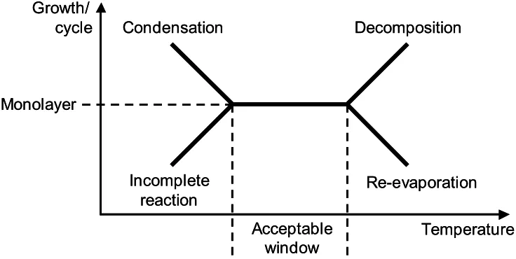
ALD reactions are typically carried out in the 200°C to 400°C temperature range. If the
deposition temperature is too high, film growth can be retarded by desorption of desired products or reactant (because chemical bonding cannot be sustained or the density of
chemically reactive sites is reduced) or film growth can be enhanced by thermal decomposition of reactants (yielding a CVD like process). If the deposition temperature is
condensation. The temperature window for maximum deposition rate is relatively wide compared to CVD processes that are much more temperature sensitive [1, 2]. Figure 3.2 schematically illustrates the allowable temperature window for ALD. Depending on the
specific chemistry involved, ALD growth rates may also be reduced by desorption of adsorbed reactants during the purge steps [3].
Precursor must be volatile and thermally stable to ensure efficient transportation so that reactions will not be precursor transportation controlled (ie, critically controlled heating of gas feed lines to minimize condensation or unwanted precursor reactions). The vapor
pressure of precursors must be high enough to completely fill the deposition chamber so that monolayer deposition takes place within a reasonable length of time (approximate vapor
pressures of 0.1 Torr). Precursors must chemisorb onto the surface or rapidly react with surface groups, such as hydroxyl group on oxide surfaces, and react aggressively with the second vapor (whether a reducing or oxidizing vapor) to keep the deposition times short.
Also, the self-limiting property of ALD will be lost if the precursor self-decomposes, etches the underlying film, or dissolve into the film.
The major limitation of ALD is its slowness: usually only a fraction of a monolayer is
deposited in one cycle. This observation is generally attributed to steric hindrance of molecular precursors adsorbing on the surface, leading to saturation at less than one full
monolayer of surface coverage [4]. Typical deposition rate are 100-300 nm h-1. Therefore, it is not very practical to grow micrometer thick films. Fortunately, due to aggressive scaling of CMOSFET devices, the films require for future generation IC devices are very thin
Intrinsic Advantages of ALD
This surface-controlled mechanism of film growth by the sequential deposition of monolayers (as discussed in the previous section) gives ALD some characteristic advantages
over more traditional CVD and PVD techniques [1, 5]. In theory, since the final film thickness depends only on the number of ALD cycles used, atomic-scale thickness control is
easily achieved (in practice, this prediction is not necessarily true for very thin films or polycrystalline materials). Because individual reactants are isolated from each other by purge or evacuation steps, highly reactive chemistries can be used, which allows for a wider
selection of precursors than that traditionally available for CVD and lower deposition temperatures [6]. Self-limiting surface reactions in ALD allow for much better uniformity
than CVD for films deposited on large-area wafers, because parts of the wafer exposed to a higher flux of reactants will not have thicker films, since the deposition during any individual pulse stops when a given area reaches saturation. Similarly, ALD deposition of sequential
monolayers leads to much better conformality than PVD for films deposited on high aspect-ratio structures, meaning that the film thickness is constant over all parts of three-dimensional structures such as deep trenches, in which shadowing effects usually hinder
PVD methods. Because of these advantages, ALD is beginning to replace CVD and PVD in the semiconductor industry for applications that require high conformality and uniformity,
such as DRAM (Dynamic Random Access Memory) cells and back-end interconnect barriers and metallization [7]. Because of its excellent thickness control and uniformity, ALD could also the best deposition method for new high dielectric constant (or high-k) gate materials