High-Performance Storage Devices of Flash
Memory flip flop using Various Techniques
Sandeep Bansal
1, Prof. Suresh. S. Gawande
2, Dr. Mohit Gangwar
3M. Tech. Scholar, Department of Electronics and Communication, Bhabha Engineering Research Institute, Bhopal, India1
Guide, Department of Electronics and Communication, Bhabha Engineering Research Institute, Bhopal, India 2 Co-guide, Department of Electronics and Communication, Bhabha Engineering Research Institute, Bhopal, India 3
ABSTRACT: Power consumption plays an import role in any integrated circuit, VLSI design and electronic device. In this paper a literature review of true single phase clocking (TSPC), clock pair shared flip flop (CPSFF) and multi threshold voltage complementary metal oxide semiconductor (MTCMOS) techniques. Among those techniques clocked pair shared flip flop consume least power than true single phase clocking flip flop. MTCMOS technique which reduce the power consumption by approximately 40% to 60% than the original CPSFF
KEYWORDS: - Flip flop, TSPC, CPSFF, and MTCMOS.
I. INTRODUCTION
With the recent popularity of various portable devices, the demand for compact and reliable NAND flash-based storage devices (NFSDs) has dramatically increased. NAND flash memory (NFM) offers many advantages, such as non-volatility, high performance, the small form factor, and low-power consumption, while rapidly improving capacity and cost by downscaling the process technology to 21 nm [1] and providing a 3-D NFM structure. NFM’s higher degree of chip integration did not compare with other types such as NOR is flash memory [2] achieved by its specialized architecture for bulk data access. In this architecture, the page—the unit for read and program operations—includes numerous memory cells. The unit for erase operations, the block, is composed of tens of pages. Page size has continuously increased since early NFMs, when a single page was smaller than 1 kB. Increasing the page size enlarges the portion of cell areas in a die and reduces the number of NFM operations that service a given amount of data. Thus, the larger page reduces the cost-per-bit of NFMs and improves the throughput of NFSDs. However, the larger page cannot guarantee better performance in all cases. In particular, the larger page causes higher fragmentation within NFMs, which causes inefficient utilization of NFM space [called false capacity (FC)] and increases the number of garbage collections (GCs) [3]. Moreover, when requests with a small amount of data are given, NFM write performance deteriorates because of frequent read-and-modify procedures
Flip-flops can be either simple (transparent or asynchronous) or clocked (synchronous); the transparent ones are commonly called latches. The word latch is mainly used for storage elements, while clocked devices are described as flip-flops. Simple flip-flops can be built around a pair of cross-coupled inverting elements: vacuum tubes, bipolar transistors, field effect transistors, inverters, and inverting logic gates have all been used in practical circuits. Clocked devices are specially designed for synchronous systems; such devices ignore their inputs except at the transition of a dedicated clock signal (known as clocking, pulsing, or strobing). Clocking causes the flip-flop to either change or retain its output signal based upon the values of the input signals at the transition. Some flip-flops change output on the rising edge of the clock, others on the falling edge. The optimization to minimize area at all costs, has only been secondary to the fixation on increasing circuit speed and again our position is that this should be examined with respect to its effect on power consumption. Some of the techniques that will be presented will come at the expense of increased silicon area and thus the cost of the implementation will be increased.
These are extremely important circuit elements in any synchronous VLSI chip. They are not only responsible for correct timing, functionality, and performance of the chips, but also their clocked devices consume a significant portion of the total active power. Based on the comparison of the power breakdown for different elements in VLSI chips, latches and flip-flops are the major source of the power consumption in synchronous systems. Latches and flip-flops have a direct impact on power consumption and speed of VLSI systems. Therefore study on low-power and high performance latches and flip-flops is inevitable. A universal flip-flop with the best performance, lowest power consumption, and highest robustness against noise would be an ideal component to be included in cell libraries. However, increasing the performance of flip-flops generally involves significant power and robustness trade-offs. The desirability of this tradeoff can only be determined with respect to a given market situation, but in many cases a moderate increase in area can have substantial impact on the power requirements. It is clear that if power reduction is more important than increasing circuit clock rate, then the area consumed by large clock buffers, power distribution busses and predictive circuit architectures would be better spent to reduce the power dissipation.
The total power consumption per device is the sum of a dynamic component from charging and discharging the capacitance and a static component from the leakage current:
P
tot
P
dyn
P
stat (1)
arf
cC
LV
DD2I
offV
DD (2)In this expression
f
cis the clock frequency andar
is the switching probability.The Clock Divider circuit has found immense application in multiple clock domain (MCD) systems like ASICs, SoC (System on Chip) and GALS (Globally Asynchronous, Locally Synchronous).SoC, which is an IC designed by stitching together multiple stand-alone VLSI designs ( called IPs) to provide full functionality for an application [l] has different IP blocks operating at different clock frequency. Clock generation and clock distribution for these MCD systems are the costliest in terms of power consumption [2].The clock generation system generates different frequencies for the clock domains from the basic crystal oscillator (tens of MHz) using PLLs(as frequency multipliers) followed by Clock Dividers. Hence minimizing the power consumption of the clock divider circuit is a crucial step in the design of Clock generator circuit for MCD systems.
II. DESIGN A PULSE TRIGGERED FLIP FLOP IN VARIOUS TECHNIQUE
feed through. This scheme actually improves the ―0‖ to ―1‖ delay and thus reduces the disparity between the rise time and the fall time delays. In comparison with other P-FF designs such as ep-DCO, CDFF, and SCDFF, the proposed design shows the most balanced delay behaviors.
III. SIMULATION RESULT
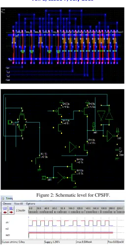
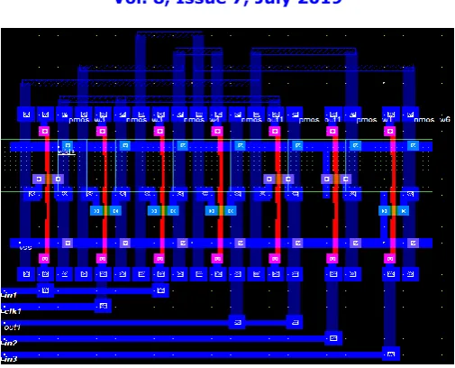
The conventional P-FF designs, CDFF, static CDFF, MHLFF, P-FF, CPSFF and MTCMOS circuits could be drawn by using the DSCH tool and verified by the level of the section in the designed circuit. The layout and the compilation could be verified using MICROWIND. DSCH and MICROWIND tools are used to carry out the work for different technologies like 25nm, 65nm and 90nm.
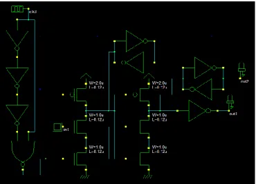
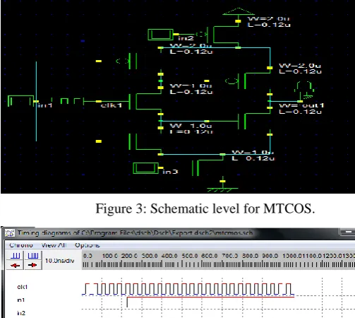
The design of all schematics, input output waveform based on DSCH and layout for all based on MICROWIND are shown below figure 1-3 respectively.
The target technology is the TSMC 90-nm CMOS process. Since pulse width design is crucial to the correctness of data capture as well as the power consumption [10]–[13], the transistors of the pulse generator logic are sized for a design spec of 120 ps in pulse width in the TT case. The sizing also ensures that the pulse generators can function properly in all process corners. With regard to the latch structures, each P-FF design is individually optimized subject to the product of power and D-to-Q delay. To mimic the signal rise and fall time delays, input signals are generated through buffers.
The latch part is almost same as that CPSFF.The latch consists of transistors. Each transistor is having its own use. Instead of using clock for recharging, a small pull-up PMOS transistor P4 is used whose input is continuously grounded. So, node X will be high most of the time. The evaluation path transistor N6 is controlled by the feedback from the output (q fdbk). Therefore, if the state of input data is same as that of output evaluation path will be turned off preventing the discharge at node X. This results in power saving when input data remains idle for more than one clock cycle. Although P4 is statically ON, it will not result in static power dissipation because as soon as the data sampling finishes and ’q’ obtains the value of ’data’, the pull down path get turned off node X is pulled back to high without any static power being dissipated. There are 3 transistors stacked in the evaluation path which less when compared with other flip flops.
Table 1: Power dissipation comparisons for different technologies
IV. C
Design Technologies
90nm 65nm 25nm
Conventional P-FF 56.466 uW 82.3 uW 5.409 uW
CDFF 1.474 mw 90.416 uw 0.641 mw
CPSFF 0.734mW 51.32uW 0.754mW
[2] Jin-Young Kim, Sang-Hoon Park, Hyeokjun Seo, Ki-Whan Song, Sungroh Yoon, and Eui-Young Chung, ―NAND Flash Memory With Multiple Page Sizes for High-Performance Storage Devices‖, IEEE Transactions on Very Large Scale Integration (VLSI) Systems, Vol. 24, No. 2, February 2016
[3] Liaqat Moideen Parakundil and N. Saraswathi, ―Low Power Pulse Triggered D-Flip Flops using MTCMOS and Self-Controllable Voltage Level Circuit‖, 2014 IEEE International Conference on Advanced Communication Control and Computing Technologies (ICACCCT).
[4] Dennis land Larsen, Pere LlimosMuntal, Ivan H. H. Jørgensen and Erik Bruun, ―High-voltage Pulse-triggered SR Latch Level-Shifter Design Considerations‖, 978-1-4799-5442-1/14/$31.00 ©2014 IEEE.
[5] Jin-Fa Lin, ―Low-Power Pulse-Triggered Flip-Flop DesignBased on a Signal Feed-Through Scheme‖, IEEE Transactions on Very Large Scale Integration (VLSI) Systems 1063–8210/$31.00 © 2013 IEEE.
[6] Guang-Ping Xiang, Ji-Zhong Shen, Xue-Xiang Wu and Liang Geng, ―Design of a Low-Power Pulse-Triggered Flip-Flop with Conditional Clock Technique‖, 978-1-4673-5762-3/13/$31.00 ©2013 IEEE.
[7] Sebastien Bernard, Alexandre Valentian, Marc Belleville, David Bol and Jean-Didier Legat, ―Design of a Robust and Ultra-Low-Voltage Pulse-Triggered Flip-Flop in 28nm UTBB-FDSOI Technology‖, 978-1-4799-1361-9/13/$31.00 ©2013 IEEE. [8] Yin-Tsung Hwang, Jin-Fa Lin, and Ming-Hwa Sheu, ―Low-Power Triggered Flip-Flop Design withConditional
Pulse-Enhancement Scheme‖, IEEE Transactions on Very Large Scale Integration (VLSI) Systems, VOL. 20, NO. 2, FEBRUARY 2012.
[9] Xue-Xiang Wu and Ji-Zhong Shen, ―Low-power explicit-pulsed triggered flip–flop with robust output‖, ELECTRONICS LETTERS 22nd November 2012 Vol. 48 No. 24.