An Improved Balanced Optical Phase-Locked
Loop Incorporating an Electro-Optic Phase
Modulator
A. Banerjee, Member IEEE
Department of Applied Electronics and Instrumentation Engineering, Academy of Technology, Adisaptagram,
Hooghly, West Bengal, India
ABSTRACT: A balanced optical phase-locked loop (OPLL) has been investigated through simulation experiment, considering the photo-detector shot noise, laser phase noise and loop propagation delay into account. This optical balanced loop contains an additional electro-optic phase modulator in the phase-locking branch to improve the tracking capability of the loop. The tracking behaviour of the OPLL are investigated in terms of pull-in behaviour and phase-error variance in presence of loop-delay. The modified loop achieves lock-in state in a relatively smaller acquisition time than the conventional OPLL. In this OPLL, the line-width requirement can be easily increased to a large value, by changing the phase control parameter.
KEYWORDS: Electro-optic phase modulator, Voltage controlled oscillator (VCO), Phase-error standard deviation (PESD), Loop-delay.
I. INTRODUCTION
Optical phase-locked loops (OPLL) are used in many applications involving frequency stabilization of a laser, clock extraction in high-speed optical communication systems, low noise microwave or mm-wave signal generation, and precise optical measurements. In the last few years, lot of works has been carried out on OPLL and in connection to its different applications. A balanced OPLL used for clock recovery at a bit rate of 160 Gbps was suggested and experimentally demonstrated [1]. Zibar et al. [2], analyzed a balanced OPLL used for clock extraction from high-speed optical time division multiplexed (OTDM) signals. The effects of loop-delay time and the laser transfer function were included in the differential equations describing the system, and a detailed timing jitter analysis was performed. A coherent receiver based on an OPLL for linear phase demodulation was presented [3]. For high-frequency operation, monolithic and hybrid integrated versions of the receiver were developed and experimentally verified in an analog link. Also, a novel phase-locked coherent optical phase demodulator with feedback and sampling was proposed and investigated for high-linearity microwave photonic links [4]. A novel coherent optical receiver based on an OPLL was presented and experimentally demonstrated to reduce the nonlinear distortion in a traditional receiver while retaining the signal to noise ratio (SNR). Up to 15-dB of spur free dynamic range (SFDR) improvement was obtained [5]. A high dynamic range phase modulated optical link using an attenuation-counter propagation photonic phase-locked loop (ACP-PPLL) was reported [6]. A modified OPLL that incorporated a frequency discriminator was proposed [7] to increase the frequency acquisition capability. Also, an OPLL incorporating a frequency down-conversion module was proposed and demonstrated [8]. The use of the frequency down-conversion module allows the use of lower-frequency components in the phase control module, which would reduce significantly the system cost. A packaged semiconductor laser OPLL for photonic generation, processing and transmission of microwave signals was implemented [9].
Microwave carriers in the range of 7-14 GHz were generated with a phase-error variance of
7 10
4 rad2 in a 15-MHz bandwidth and 0.4 ns loop-delay condition. Also, a high purity mm-wave optical-beat signals at frequencies up to 330.566 GHz was generated [10].higher value of the loop natural frequency due to the stability condition [11]. Secondly, the phase-error variance even at the optimum condition rises sharply with the delay. Lowering of the loop natural frequency has cascading effects on the loop performance, namely, it decreases the pull-in range, increases the pull-in time, increases tracking error, increases the phase-error variance etc. The loop propagation delay induces a phase delay at the output of the local oscillator (LO) VCO. This can be minimized by advancing the phase of the LO through an external control by means of a phase modulator [12], [13].
In order to be able to control the parameters viz., loop stability, frequency pulling time, and loop gain, a modified balanced OPLL having an additional arrangement for phase modulation is proposed in this paper. The modified balanced OPLL is studied through simulation experiment, considering the photo-detectors shot noise and laser phase noise in presence of loop propagation delay. The analyses are made in terms of pull-in time and phase-error standard deviation (PESD) in presence of loop-delay time. The loop parameters are properly chosen for this simulation experiment.
II. SYSTEMDESCRIPTION
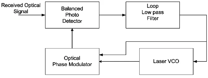
The block diagram of a modified balanced optical phase-locked loop is shown in Fig. 1. This modified OPLL contains all the components of a standard balanced loop in addition of an extra electro-optic phase modulator [14], [15]. The received optical signal and the phase modulated optical signal are combined by an optical coupler, and the resulting optical signal is converted in the electrical domain by two balanced photodiodes. The trans-impedance amplifier provides impedance matching. The electrical signal at the loop amplifier output is then processed by a standard first-order active filter, and finally sent to the VCO laser input [16]. The electro-optic phase modulator is then used to modulate the phase of the optical signal at the VCO laser output. When OPLL is locked, the loop tracks the incoming signal frequency and phase.
Fig. 1 Block schematic of a modified balanced optical phase-locked loop.
III.THEORETICALBACKGROUND
In this section, we describe the theory of modified balanced optical phase-locked loop. Consider a modified balanced OPLL as shown in Fig.1. The received optical signal can be expressed as
sin
R R R nR
E
t
P
t
t
(1)where
P
R is the received optical signal power (W),
R is the angular frequency (rad/s) of the received signal and
nRt
is the phase noise of the transmitter laser source. The LOlaser signal after phase modulation can be written as
0
( )
0cos
0L L L PM VCO nLO
where
P
L0 is the LO laser power (W),
LO is the angular frequency (rad/s) of the LO laser signal and
nLO
t
is the phase noise of the LO laser source. In (2),
VCO
t
is phase modulation of the local laser VCO due to the input to the VCO terminal, and
PM( )
t
is phase modulation of the local laser VCO due to the phase modulation of the phasemodulator.
The optical coupler, being a symmetrical 180°/3-dB device, generates the sum and difference of its input fields
1
1
2
R LOE
E
E
(3A)
2
1
2
R LOE
E
E
. (3B)Illuminating the surface of a photodiode with an optical field
E
will lead to a current of
i
PD
R E
2 (4)flowing through the diode. In (4),
R
is the photo-detector responsivity (A/W). Using equations (1)-(4), the balanced photo-detector output is expressed by
V t
K
PDsin
E
t
n t
(5)where
E
t
R
L0
t
PM
t
VCO
t
nR
t
nLO
t
is the phase-error at the output ofthe detector and
n t
is the shot noise associated with the photo-detectors. The expression0
2
PD T R L
K
RR
P P
(6)is the photo- detector gain (V/rad) of the OPLL, where
R
T is the trans-impedance (
).Consider a standard first-order active loop filter with transfer function
1 21
s
s
s
F
, where
1 and
2 are filtertime constants. If its output is
V
f
t
, then it is related to its inputV
t
, by the following equation
t
V
dt
t
dV
dt
t
dV
f
1
2
. (7)Now, the different phase modulation components of the VCO laser source are given by [17]
t
VCO
t
K
VCOV
ft
dt
(8)
PM
t
K V t
PM f
(9)where
K
VCO is the VCO laser sensitivity,K
PM is the electro-optic phase modulator sensitivity (rad/V) and
(second) is the loop-delay.
2,
PNS
f
f
0
f
(10)where
S
PN
f
(rad2/Hz) is the one-sided PSD of the phase noise stemming from the white frequency noise, and
(Hz) is the full-width-half-maxima (FWHM) of the transmitter and VCO laser line-width.The PSD of the shot noise is represented by [19]
2
2
,
SN T R LO
S
f
qRR
P
P
0
f
(11) whereS
SN
f
is the one-sided PSD (V2/Hz) of the shot noise andq
is the electron charge (1.6 10
9C).IV.SIMULATION RESULTS
The proposed OPLL is numerically simulated using MATLAB software. In simulation experiment, the balanced OPLL is modelled taking strong nonlinearity of the loop in the presence of loop-delay. Both phase noise and shot noise are assumed to be White Gaussian noise. Polar Marsaglia method [20] is used to generate laser phase noise and photo-detector shot noise. The loop-delay is included in the simulation programme as a delay to the phase-error signal of the phase detector output to control the VCO laser frequency. For the simulation study, the expression given by (7) can be written as
2
2
1 1
f f
t
V
t
t
V
t
V t
V t
t
(12)where
t
is the sampling interval. In (12),V
f
t
,V
f
t
t
are the loop filter output voltage at t-th and
t
t
-th instant of time, respectively andV t
,V t
t
are the balanced detector output at t-th and
t
t
-th instant of time, respectively. To obtain the value of
VCO
t
, the integration in (8) is done applying 4th order Runge-Kutta method [21].The simulation results shown in this section are obtained by the time domain numerical model of the modified balanced OPLL. The numerical model of the modified OPLL is based on equations (1)-(12). The operating frequencies of the lasers are very high (~ few hundred THz). Thus, for simulation study, large number of sampling points is required in time domain analysis. For this purpose, large number of computer memory is needed which is not available. To overcome this difficulty, the operating frequencies of the optical sources are scaled down to 100 kHz and so, laser line-width is taken of the order of few kHz.
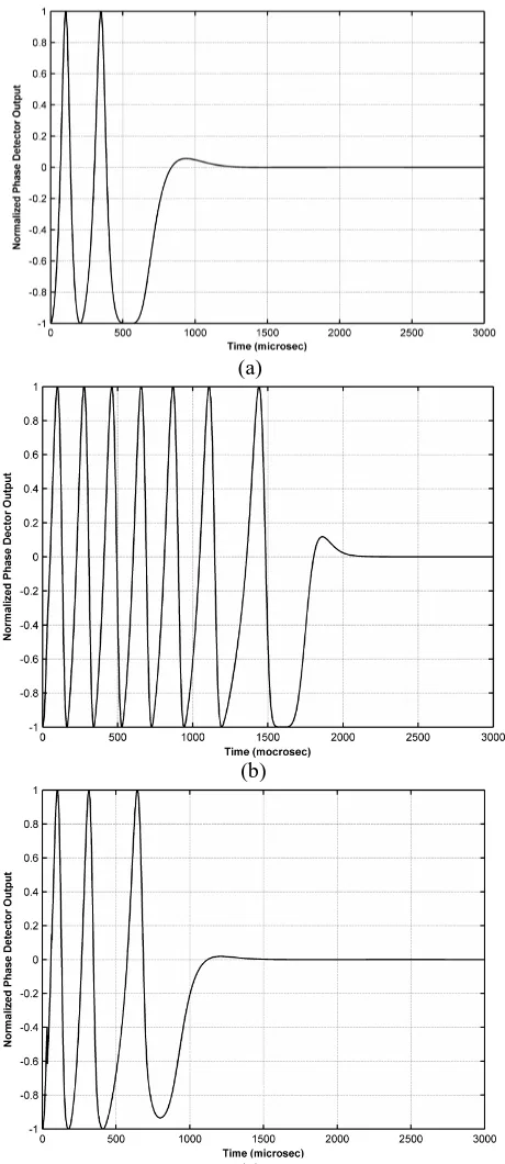
In optical communication systems, the problem is the fluctuation of the beat angular frequency of the optical sources. The pull-in limit must be as large as possible. For pull-in behaviour analysis, we neglect the shot noise components including phase noise and the loop is operating in the unlocked mode, i.e., the incoming signal frequency is not equal to the VCO laser free-running signal frequency. The normalized photo-detector output voltage is plotted against time as shown in Fig. 2. From three figures it is observed that in Fig. 2(a) the loop achieves lock-in state after a few number of cycle slips than in Fig. 2(b), because in second case the OPLL is delay limited with 20 ns loop propagation delay. Also, in Fig. 2(c), the lock-in condition reaches after a fewer number of cycle slips due to extra phase modulator present in the loop.
In the simulation analysis, the phase-error standard deviation (PESD) is calculated taking the phase noise, shot noise and loop-delay into account. Under locked state, the PESD is calculated at the balanced photo-detector output. Dependence of tracking capability of the loop on loop propagation delay is shown in Fig. 3, showing the effect of extra phase modulator control on the loop behaviour. It is found that PESD increases with the increase of loop-delay. Consider PESD as 7, the allowable loop-delay, for stable operation of the OPLL, is increased from 1 ns to 7 ns with
PM
(a)
(b)
(c)
Fig. 3 Phase-error standard deviation versus loop propagation delay. Phase modulator sensitivity is used as a parameter. Simulation results are shown by the circles.
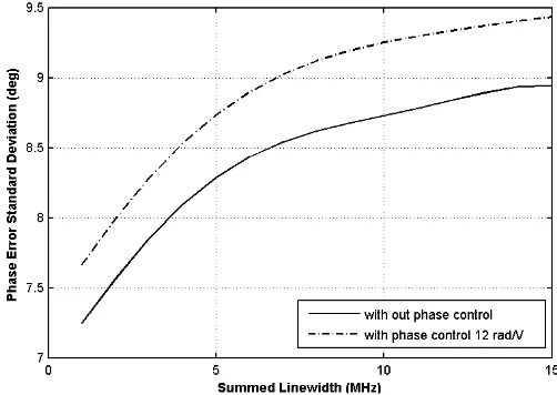
Fig. 4 Phase-error standard deviation as a function of summed laser linewidth for 10 ns loop-delay. Phase modulator sensitivity is used as a parameter.
Fig. 4 represents the PESD plotted against the sum of the line-widths of the transmitter and local oscillator lasers. From this figure, it is concluded that PESD increases with the increase of summed lasers line-width. In presence of 10 ns loop-delay, the PESD reduces about 1.3º in presence of the phase modulator with sensitivity
K
PM
12
rad/V, at source laser line-width
S
2.5 MHz and local oscillator line-width
LO
2.5
MHz. As observed from Fig. 4,V. CONCLUSION
A simulation study of a modified balanced OPLL has been performed considering into account photo-detector shot noise, VCO phase noise in the presence of loop propagation delay. This modified OPLL contains all the components of a standard balanced OPLL in conjunction of an additional electro-optic phase modulator in the phase-locking branch. The additional phase modulator has been added at the output of the laser VCO to improve the tracking capability of the loop by providing the additional negative frequency feedback. It has been found that the loop achieves lock-in state in a relatively smaller time than the conventional loop. Considerable reduction in phase-error standard deviation has been achieved by properly changing the phase modulator control parameter. In this modified loop, by adjusting the phase control parameter, the line-width requirement can be easily increased to a large value without crossing the stability limit. So this modified OPLL is preferable for the optical sources having larger line-width, i.e., commercially available DFB lasers (line-width ~ 2-20 MHz).
REFERENCES
[1] D. Zibar, L. K. Oxenlowe, A. T. Clausen, and J. Mork, “Theoretical and experimental investigation of a balanced phase-locked loop based clock recovery at a bit rate of 160 Gb/s,” presented at the IEEE Laser Electro Optics Soc. (LEOS) Conf., Tucson (2003).
[2] D. Zibar, J. Mork, L. K. Oxenlowe, and A. T. Clausen, “Phase noise analysis of clock recovery based on an optoelectronic phase-locked loop,”
J. Lightw. Technol., vol. 25, pp. 901-914 (2007).
[3] A. Ramaswamy et al., “Integrated coherent receivers for high-linearity microwave photonic links,” J. Lightw. Technol., vol. 26, pp. 209-216 (2008).
[4] D. Zibar et al., “Phase-locked coherent demodulator with feedback and sampling for optically phase-modulated microwave links,” J. Lightw. Technol., vol. 26, pp. 2460-2474 (2008).
[5] H. F. Chou et al., “SFDR improvement of a coherent receiver using feedback,” Proc. IEEE, paper CFA3 (2006). [6] Y. Li and P. Herczfeld, “Coherent PM Link Employing ACP-PPLL,” J. Lightw. Technol., vol. 27, pp. 1086-1094 (2009).
[7] Z. F. Fan and M. Dagenais, “Optical generation of a mHz-linewidth microwave signal using semiconductor lasers and a discriminator-aided phase-locked loop,” IEEE Trans. Microw. Theory Tech., vol. 45, pp. 1296-1300 (1997).
[8] H. Rideout, J. Seregelti, S. Paquet, and J. P. Yao, “Discriminator-aided optical phase-locked loop incorporating a frequency down-conversion module,” IEEE Photon. Technol. Lett., vol. 18, pp. 2344-2346 (2006).
[9] L. N. Langley, M. D. Elkin, and A. J. Seeds, “Packaged semiconductor laser optical phase-locked loop for photonic generation, processing and transmission of microwave signals,” IEEE Trans. Microw. Theory Tech., vol. 47, pp. 1257-1264 (1999).
[10] M. Hyodo and M. Watanabe, “Optical generation of mm-wave signals of up to 330 GHz by means of cascadingly phase locking three semiconductor lasers,” IEEE Photon. Technol. Lett., vol. 15, pp. 458-460 (2003).
[11] M. A. Grant, W. C. Michie, and M. J. Fletcher, “The performance of optical phase locked loops in the presence of non-negligible loop propagation delay,” J. Lightw. Technol., vol. LT-5, pp. 592-597 (1987).
[12] A. Acampora, and A. Newton, “Use of phase subtraction to extend the range of a phase-locked demodulator,” RCA Rev., vol. 27, pp. 577-599 (1966).
[13] B. N. Biswas, A. P. Sinha, P. Lahiri and D. Mondal, “A novel optical phase locked loop,” Proc. XXV GA URSI, Kyota, Japan (1993). [14] Y. Li et al., “Novel phase modulator linearity measurement,” IEEE Photon. Technol. Lett., vol. 21, pp. 1405-1407 (2009).
[15] K. Noguchi, O. Mitomi, and H. Miyazawa, “Millimeter-wave Ti:LiNbO3 optical modulators,” J. Lightw. Technol., vol. 16, pp. 615-619 (1998).
[16] G. L. Abbas, V. W. S. Chan, and T. K. Yee, “Local-oscillator excess noise suppression for homodyne and heterodyne detection,” Opt. Lett., vol. 8, pp. 419-421 (1983).
[17] F. M. Gardner, Phaselock Techniques, 2nd ed. New York: Wiley, 1979.
[18] C. H. Henry, “Phase noise in semiconductor lasers,” J. Lightw. Technol., vol. LT-4 (1986). [19] M. Ohtsu, Highly Coherent Semiconductor Lasers, 1st ed. Boston, MA: Artech House, 1992.