ISSN(Online): 2320-9801
ISSN (Print): 2320-9798
International Journal of Innovative Research in Computer
and Communication Engineering
(An ISO 3297: 2007 Certified Organization)
Vol. 3, Issue 7, July 2015
Design and Analysis of D Flip Flop Using
Different Technologies
Hardeep Kaur, Er.Swarnjeet Singh, Sukhdeep Kaur
M.Tech Student, Dept. of ECE, Baba Farid College of Engineering &Technology, Bathinda, Punjab, India
Assistant Professor, Dept. of ECE, Baba Farid College of Engineering &Technology, Bathinda, Punjab, India
M.Tech Student, Dept. of ECE, Baba Farid College of Engineering &Technology, Bathinda, Punjab, India
ABSTRACT : The field of digital electronics has been directly towards to the low power digital system. The use of very large scale integration technology in high performance computing, wireless communication, consumer electronics has been rising at a very fast rate. The challenge for VLSI technology is growing in leakage power consumption. Wide utilizations of memory storage systems in modern electronics triggers a demand for high performance and low area implementation of basic memory component and one of the most state holding element is D Flip Flop. In this paper analysis of power, delay, area and power delay product is done for D flip flop using different technologies like static CMOS, C2MOS, POWER PC, GDI MUX, TSPC, etc. Low power Flip flops are useful for the design of low power digital system. The analysis and the comparison is done using TANNER EDA Tool at 130nm Technology.
KEYWORDS: Low power, CMOS, C2MOS, ,GDI MUX,TSPC, D Flip Flop, POWER PC
I. INTRODUCTION
In the past, the major concerns of vlsi designers were area, cost, performance and reliability. Low power dissipation became a highly design concern and become more important as we move to all mobile computing and communications. The latest advancement in computing technology has set up a goal for high performance with low power consumption for vlsi designers. Flip flops are important state holding and timing elements in digital circuits. The performance of D flip flop is much important to conclude the performance of the whole circuit. With increasing use of mobile devices, consumer electronics market demands a stringent constraint on reducing power consumption. Designers are striving for small area, low power and higher speed due to increasing demand of portable devices. Several researchers have worked on flip flops but they focus on one or few types of flip flops and applications. The need for comparing different design is the main motive of this paper. In this D flip flop is designed by using different techniques like Static CMOS,
C2mos(clocked cmos).GDI MUX,DSTC,POWER PC and TSPC etc by using130nm and simulations is done using
Tanner EDA.
II.REGIONS OF FLIP FLOP OPERATION
There are three regions of flip flop operation and in which one is acceptable for functioning correctly. The regions are as follows:-
Stable Region-In this region the set up and hold time of a flip flop are met and in this the clock to Q delay is not dependent to D to clock delay.
Metastable region- in this region as D to clock delay is decreases at a certain point the clock to Q delay rising and ends to failure, which are difficult to debug in real circuits.
Failure Region-In this region the changes in data are unable to be transferred to the output of the flip flop.
ISSN(Online): 2320-9801
ISSN (Print): 2320-9798
International Journal of Innovative Research in Computer
and Communication Engineering
(An ISO 3297: 2007 Certified Organization)
Vol. 3, Issue 7, July 2015
Fig.1-Operation regions of DFF
II. IMPLEMENTATION OF D FLIP FLOP USING DIFFERENT TECHOLOGIES
A. Static CMOS (complementary metal oxide semiconductor)-It consist of nMOS pull down and pMOS pull up transistors together in a complementary way. The circuit diagram of Static CMOS based DFF as follows in figure 2.
ISSN(Online): 2320-9801
ISSN (Print): 2320-9798
International Journal of Innovative Research in Computer
and Communication Engineering
(An ISO 3297: 2007 Certified Organization)
Vol. 3, Issue 7, July 2015
In this circuit 1.5 v voltage is used and simulated using Tanner EDA at 130nm Technology. The output waveform of Static CMOS Based DFF is shown Figure 3.
Fig.3-Output waveform of Static CMOS based DFF
B.C2MOS(Clocked CMOS) Based D Flip flop- clocked cmos is composed of a static logic circuit with tristate output network (made up of FET’s M1 and M2) that is controlled by Ø and Ø bar. When Ø=0 both M1 and M2 are active and become a standard static logic state. And when Ø=1 both M1 and M2 are cut off as shown in figure 4.
ISSN(Online): 2320-9801
ISSN (Print): 2320-9798
International Journal of Innovative Research in Computer
and Communication Engineering
(An ISO 3297: 2007 Certified Organization)
Vol. 3, Issue 7, July 2015
The schematic diagram of implementation of D flip flop using clocked CMOS is shown in figure 5 .
Fig.5- c2mos based DFF
The output waveform of Clocked CMOS based D flip flop is shown in Figure.6
ISSN(Online): 2320-9801
ISSN (Print): 2320-9798
International Journal of Innovative Research in Computer
and Communication Engineering
(An ISO 3297: 2007 Certified Organization)
Vol. 3, Issue 7, July 2015
C.GDI MUX (Gate Diffusion Input Multiplexer)- GDI multiplexers are composed of single pair of transistors and cross coupled pair of Invertors. First multiplexer is connected to the system clock and its inputs are connected to D input and feed back loop. The schematic diagram of GDI MUX based D Flip Flop is shown in figure 7.
Fig.7-GDI MUX based DFF
This topology creates a Positive edge triggered flip flop with reduced propagation delay. The output waveform of GDI MUX based DFF is shown in figure 8.
ISSN(Online): 2320-9801
ISSN (Print): 2320-9798
International Journal of Innovative Research in Computer
and Communication Engineering
(An ISO 3297: 2007 Certified Organization)
Vol. 3, Issue 7, July 2015
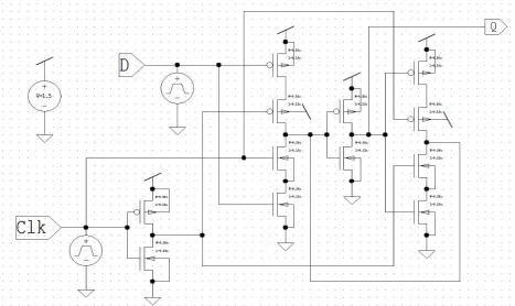
D. POWER PC-The main advantage of POWER PC D flip flop is short circuit path and low power feedback.The circuit diagram of D Flip flop using POWER PC is shown in figure 9.
Fig.9- POWER PC based DFF
The output waveform of POWER PC based DFF is shown below in figure 10.
ISSN(Online): 2320-9801
ISSN (Print): 2320-9798
International Journal of Innovative Research in Computer
and Communication Engineering
(An ISO 3297: 2007 Certified Organization)
Vol. 3, Issue 7, July 2015
E. TSPC (True single phase clocked )- In TSPC logic we have only clock and do not need an inverted clock. These techniques eliminate skew problems due to different clock phases. The circuit diagram of TSPC based D flip flop is shown in figure 11.
Fig.11- TSPC based DFF
The output waveform of TSPC based D flip flop is shown in figure 12.
ISSN(Online): 2320-9801
ISSN (Print): 2320-9798
International Journal of Innovative Research in Computer
and Communication Engineering
(An ISO 3297: 2007 Certified Organization)
Vol. 3, Issue 7, July 2015
The comparison of D flip flop using these different technologies is shown in Table 1.
Table.1-Comparison table of DFF using different techniques at 130nm
All these designs and simulations are done using TANNER EDA at 130nm Technology.
IV. CONCLUSION
It is concluded from power dissipation comparison that power pc has lowest power dissipation at 130nm.and in propagation delay comparison TSPC has least propagation delay and also concluded from transistor count comparison TSPC has less transistor count..So it is better to use TSPC logic style to design a system where fast speed is required. The electronic circuit designed with TSPC logic style will occupy less space on chip. TSPC has best performance in terms of power, speed at lower supply voltages.
REFERENCES
1) Vladimir Stojanovic and Vojin G. Oklobdzija, “Comparative Analysis of Master–Slave Latches and Flip-Flops for High-Performance and Low-Power Systems”, IEEE Journal of Solid-state Circuits , Vol. 34, No. 4, 1999
2) M. Alioto and G. Palumbo, “Modeling and Optimized Design of Current Mode MUX/XOR and D Flip-Flop”, IEEE Transactions on Circuits and Systems,Vol. 47, No. 5, 2000
3) Morgenshtein, A. Fish, I.A. Wagner, “Gate-Diffusion Input (GDI) – A Power Efficient Method for Digital Combinatorial Circuits,” IEEE Transactions,Vol. 10, No. 5, pp. 566-581, 2002
4) Po-Hui Yang, Jinn-Shyan Rang and Yi-Ming Wang, “A 1-GHz Low-Power Transposition Memory Using New Pulse Clocked D Flip-Flops”, ISCAS,IEEE International Symposium on Circuits and Systems, 2000
5) Mohamed Elgamel, Tariek Darvish and Magdy Bayoumi”Noise tolerant low power TSPCL D flip flops”, ICSAS,IEEE,2002 6) Morgenshtein, A. Fish, I.A. Wagner,”An efficient implementation of D flip flop using GDI Technique,”IEEE,2004 7) Ahmed Sayed and Hussain Al-Asaad,” A new low power high performance flip flop”,IEEE ,2006
8) Sagi Fisher,Adam Teman, Dmirity Vaysman, Alexander Gertsman,Orly Yadid Pecht,”Ultra low power subthreshold flip flop design,”IEEE, 2009
9) .Douglous A. Pucknell, Kamran Eshraghian,” Basic VLSI design third edition,2013.
S.No. DESIGN STYLE POWER
DISSIPATION (µW) PROPAGATION DELAY (nsec) FIGURE OF MERIT (µ-nJ) NO. OF TRANSISTORS
1 CMOS 2 4.94 9.88 18
2 CCMOS 0.52 4.71 2.4492 14
3 GDI MUX 2.43 2.78 6.7554 12
4 POWER PC 0.09 30 2.7 20