ABSTRACT
High Performance Integrated Controller with Variable Frequency
Control for Switching DC-DC Converters
by
Xiaoming Duan
A dissertation submitted to the Graduate Faculty of North Carolina State University
In partial fulfillment of the Requirements for the degree of
Doctor of Philosophy
Electrical Engineering
Raleigh, NC 2006
Approved by:
________________________ _______________________ Dr. Mesut E. Baran Dr. Kevin G. Gard
To my wife,
Manjing Xie
and my parents,
BIOGRAPHY
ACKNOWLEDGEMENTS
I wish first to thank my advisor, Dr. Huang, who brought me into this research area and continuously supported me throughout the last five years. He provided me with the opportunity to explore the diverse area from devices, integrated circuits to power electronics. I especially appreciate his broad vision, professional insight and warmth of character. I would also like to extend my gratitude to Dr. Baran, Dr. Gard and Dr. Ghovanloo, for serving on my committee. Their knowledge in different fields is precious resources to my research work.
My academic path in US extended from Virginia Tech (2001-2004) to North Carolina State University (2004-2006). I am indebted to the past friends and colleagues in Virginia Tech, especially, Mr. Nick Sun, Dr. Xin Zhang, Dr. Yunfeng Liu, Mr. Meng Yu, Dr. Bin Zhang, Mr. Hongfang Wang, for their stimulating conversations and friendship.
The two years in NCSU were the most productive and happy time for me. Here, I would like to express my special thanks to Mr. Jinseok Park and Mr. Ding Li. Mr. Jinseok Park is not only a great partner, but also a friend who is always ready to provide me help and encouragement. It would not be possible to complete the research project without his contributions. Mr. Ding Li’s selfless help on experiments is indispensable for my accomplishment.
etc. Together we went through the hardship of transferring from Blacksburg to Raleigh and shared the good times working and studying in this newly established center.
My heartfelt thanks belong to my wife, Manjing Xie. She supports me with her brilliant ideas and soothing cares. Her love accompanies me going through ups and downs.
Table of Contents
List of Figures... ix
List of Tables ... xii
Chapter 1 Introduction ... 1
1.1 Power consumption in high performance computer systems ... 1
1.2 Power distribution and voltage regulators in computer systems... 2
1.3 Tradeoff between high efficiency and fast load transient response... 5
1.4 Research motivations ... 8
1.5 Outline of dissertation ... 11
Chapter 2 Current Mode Variable Frequency Control... 13
2.1 Background and review of conventional PWM control ... 13
2.2 Design considerations of load transient response ... 20
2.3 Design with adaptive voltage positioning... 24
2.4 Control with variable switching frequency... 27
2.4.1 Constant on time control ... 28
2.4.2 Frequency regulation at steady state ... 28
2.5 Proposed control scheme with variable switching frequency ... 30
2.5.1 System architecture... 30
2.5.2 AVP design... 32
2.5.3 Small signal analysis ... 34
2.5.4 Comparison with peak current control... 40
2.5.5 Power efficiency and control bandwidth ... 44
2.5.6 Bandwidth limitations... 48
Chapter 3 Integrated Controller for Switching DC-DC Converters
... 51
3.1 Introduction ... 51
3.2 Design methodology of control circuits ... 54
3.3 Noise issue in integrated controllers... 57
3.4 Current sensing design... 62
3.5 Overview of the implemented controller ... 68
3.6 Summary of Chapter 3... 69
Chapter 4 Fully Differential Control Core Circuits ... 71
4.1 Introduction ... 71
4.2 Current sensing amplifier... 72
4.3 Voltage error amplifier ... 78
4.4 Constant on time modulator... 82
4.5 Summary of Chapter 4... 87
Chapter 5 Design of Interleaving and Current Sharing... 88
5.1 Multi-channel DC-DC converters ... 88
5.2 Multi-channel interleaving ... 91
5.2.1 Review of interleaving design... 91
5.2.3 Proposed interleaving design ... 95
5.3 Multi-channel current sharing ... 100
5.3.1 Review of current sharing design ... 100
5.3.2 Proposed current sharing design ... 102
5.3.3 Analysis of the current sharing loop ... 106
5.4 Summary of Chapter 5... 107
Chapter 6 Simulation and Experimental Verification ... 109
6.1 Prototype design... 109
6.2 System simulation... 112
6.4 Summary of Chapter 6... 121
Chapter 7 Conclusion and Future Work... 122
7.1 Conclusion ... 122
7.2 Future work... 124
List of Figures
Figure 1.1 Trends of current, voltage and technology feature size of Intel’s
microprocessor... 2
Figure 1.2 Power management system in a mobile computer ... 4
Figure 1.3 A multi-channel DC-DC converter for powering microprocessors ... 4
Figure 1.4 Average power distribution in a mobile computer ... 5
Figure 1.5 Power loss breakdown in a VRM with input voltage 12 V,... 6
Figure 1.6 Measure efficiency vs. output current of a VRM [Ren’05-1] ... 7
Figure 1.7 VRM components and CPU socket on the motherboard... 8
Figure 1.8 Variable switching frequency changing with load current... 11
Figure 1.9 Plot of frequency versus time in variable frequency control... 11
Figure 2.1 Block diagram of a DC-DC converter... 13
Figure 2.2 An implementation of voltage mode PWM control ... 15
Figure 2.3 An implementation of peak current control... 16
Figure 2.4 An implementation of active droop control... 16
Figure 2.5 System block diagram of a DC-DC converter with voltage mode control... 17
Figure 2.6 System block diagram of a DC-DC converter with peak current control ... 18
Figure 2.7 Sampling control signal with constant ramp signal... 21
Figure 2.8 Output filter and current waveforms during transient ... 22
Figure 2.9 Simplified connection between VRM and CPU on motherboard ... 24
Figure 2.10 A circuit model of power delivery network between VRM and CPU ... 24
Figure 2.11 Transient voltage waveforms w/ and w/o AVP design ... 25
Figure 2.12 The load line of the output voltage... 25
Figure 2.13 Partial model of the power delivery network ... 26
Figure 2.14 Plots of impedance for AVP design ... 27
Figure 2.15 System schematics with proposed control scheme... 31
Figure 2.16 Simplified diagram showing two control loops... 32
Figure 2.17 Frequency characteristics of the two control loops ... 32
Figure 2.18 Simplified system block diagram for AVP design ... 34
Figure 2.19 Small signal model of proposed control scheme ... 35
Figure 2.20 Plot of the voltage loop gain and the current loop gains ... 36
Figure 2.21 Bode plot of open loop gains... 37
Figure 2.22 Current transient waveforms under small and larger perturbations ... 38
Figure 2.23 Simplified feedback loop to analyze transient response... 39
Figure 2.24 Comparison of results of circuit simulation and model simulation at transient ... 40
Figure 2.25 Simulation diagram for proposed control... 41
Figure 2.26 Simulation diagram for peak current control... 41
Figure 2.27 Simulation waveforms with output capacitance of 1 mF ... 42
Figure 2.28 Internal control signals in two systems (Co=1mF) ... 43
Figure 2.29 Simulation waveforms with output capacitance of 0.4 mF ... 43
Figure 2.30 Efficiency versus switching frequency... 47
Figure 2.31 Efficiency versus output capacitance ... 48
Figure 3.2 Block diagram of a commercial controller chip (HIP6301) ... 53
Figure 3.3 A voltage subtraction circuit implemented with OpAmp... 55
Figure 3.4 A current subtraction circuit... 56
Figure 3.5 The parasitic elements that generate noise in current and voltage sensing ... 58
Figure 3.6 Measured signals at inputs of current sensor... 59
Figure 3.7 Sub-harmonic switching caused by noise in error signal ... 59
Figure 3.8 The circuit model showing parasitic elements in ground connection ... 60
Figure 3.9 Current sensing method – sense inductor current with a resistor... 63
Figure 3.10 Current sensing method – sense switch current with a resistor... 63
Figure 3.11 Current sensing method –inductor DCR sensing ... 65
Figure 3.12 Current sensing method - improved DCR sensing ... 65
Figure 3.13 Current sensing method – alternative implementation of DCR sensing ... 66
Figure 3.14 Current sensing method – sense switch current by Rdson ... 67
Figure 3.15 Current sensing method – sense switch current with sensor FET ... 67
Figure 3.16 Circuit block diagram of implemented controller ... 68
Figure 4.1 Control core circuits in the controller... 72
Figure 4.2 Circuit structure of current sensing amplifier... 73
Figure 4.3 Input stage of current sensing amplifier ... 74
Figure 4.4 Input and output waveforms of the current sensor ... 74
Figure 4.5 Frequency response of input stage in current sensing amplifer ... 75
Figure 4.6 Transconductor stage of current sensing amplifier ... 76
Figure 4.7 Gain linearity of the transconductor stage... 76
Figure 4.8 Frequency response of transconductor stage... 77
Figure 4.9 Simulation waveforms of current sensing amplifier ... 78
Figure 4.10 Circuit structure of voltage error amplifier ... 79
Figure 4.11 Input stage of voltage error amplifier... 80
Figure 4.12 Gain cell in voltage error amplifier ... 81
Figure 4.13 Transconductance vs. bias current in voltage error amplifier ... 81
Figure 4.14 Frequency response of voltage error amplifier... 82
Figure 4.15 Conventional implementation of PWM modulator ... 83
Figure 4.16 Modulator designed for proposed control scheme ... 83
Figure 4.17 Current comparator with injected offset for error correction ... 84
Figure 4.18 Simulation waveforms showing error correction by injecting offset current 85 Figure 4.19 Voltage-controlled delay block ... 86
Figure 4.20 A transconductor with linear gain determined by R1... 86
Figure 5.1 Simplified diagram of a two-channel DC-DC converter... 88
Figure 5.2 Two DC-DC converters in parallel with divided output capacitors ... 89
Figure 5.3 Simplified model of two-channel DC-DC converter... 89
Figure 5.4 Simulation waveforms with and without current sharing... 91
Figure 5.5 Clock signals with phase shifts ... 92
Figure 5.6 Ripple reduction from interleaving ... 92
Figure 5.7 Calculated ripple cancellation v.s. duty cycle ... 92
Figure 5.8 Duty cycle generated from shifted ramp signals ... 93
Figure 5.9 A circuit to generate interleaved ramp signals from a clock signal ... 94
Figure 5.10 A circuit to split the clock signal... 94
Figure 5.12 A multiplexer to generate interleaved duty cycle signals... 96
Figure 5.13 Timing diagram of the switching signals ... 97
Figure 5.14 The current and the voltage feedback signals used in the control ... 98
Figure 5.15 Ideal interleaving (a) and imperfect interleaving with unstable control signal (b)... 99
Figure 5.16 Current sharing design with peak current control ... 101
Figure 5.17 Current sharing design with common current bus... 102
Figure 5.18 Current sharing design by adjusting the level of ramp signals... 102
Figure 5.19 Current sharing design with on time modulation ... 103
Figure 5.20 Adjusting on time for current sharing ... 104
Figure 5.21 Schematic of gain stage and on time modulator for current sharing... 105
Figure 5.22 Small signal model to analyze system dynamics of current sharing control106 Figure 6.1 Microphotograph of the controller chip ... 110
Figure 6.2 Pin-out of the prototype controller ... 110
Figure 6.3 Transient simulation results... 112
Figure 6.4 Simulation of mode transition between active mode and sleep mode... 113
Figure 6.5 Simulation with input voltage varying from 20 V to 5 V... 114
Figure 6.6 Simulation of dynamic reference voltage... 114
Figure 6.7 Test board for the controller ... 115
Figure 6.8 Active mode Vin=12V, Vout=1.2V, Io=10A... 116
Figure 6.9 Sleep mode, Vin=5V, Vout=1.2V, Io=5A... 116
Figure 6.10 The output voltage ripple: Vin=12V, Vo=1V ... 117
Figure 6.11 Transition between active mode and sleep mode ... 117
Figure 6.12 VID step-up transition ... 118
Figure 6.13 VID step-down transition ... 118
Figure 6.14 Load transient: Vin=12V, Vout=1.2V, Io=0~40A ... 119
Figure 6.15 The trajectory of output voltage and load current ... 119
Figure 6.16 Steady-state switching frequency v.s. input voltage ... 120
List of Tables
Table 2.1 Transfer function gains in small signal models ... 19
Table 2.2 Parameters for control system design ... 40
Table 2.3 The list of parameters to calculate the efficiency ... 46
Table 6.1 Specification parameters of the designed VRM controller... 109
Table 6.2 Pin descriptions of the controller chip ... 111
Table 6.3 List of components used in the test... 115
Chapter 1 Introduction
1.1 Power consumption in high performance computer systems
In modern computer systems, great amount of power is consumed by the digital core chips for intensive data computation. A good example of such chips is the high performance microprocessor (CPU). When transistor technology moves into the nanometer scale, power demand of microprocessors could be even higher because more transistors are integrated and the leakage current of the transistor increases [Agerwala’05]. Another driving force of increasing power consumption in digital core chips is demand of high throughput in the computing devices. For example, the clock frequency in Intel’s CPUs has been continuously increased for three decades to improve the system performance.
supply designers, it is a nightmare to supply such huge dynamic current with the voltage tightly regulated [Lee’99]. Besides, due to the parasitic components inside the package and the chip, stabilizing voltage inside the chip is also troublesome even though the voltage outside the chip is constant. As we know, the supply voltage is crucial for maintaining chip functionality. The voltage higher than the top limit may physically damage the chip, and the voltage under the bottom limit may violate the delay requirement of the digital circuits [Saint-Laurent’04].
Figure 1.1 Trends of current, voltage and technology feature size of Intel’s microprocessor
1.2 Power distribution and voltage regulators in computer systems
Switching DC-DC converters Switching DC-DC converters
Figure 1.2 Power management system in a mobile computer
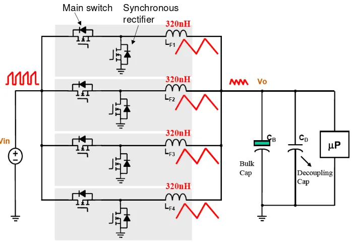
Main switch Synchronous rectifier
1.3 Tradeoff between high efficiency and fast load transient response High efficiency and fast load transient response are two major requirements in high current DC-DC converters design [Panov’01].
Although power efficiency of the switching converters is considered high compared with other voltage regulators such as the linear regulator and the switching capacitor regulator, power loss in the power supply circuits adds up to be a significant portion of total power consumption in the computer system. From experimental results shown in Fig. 1.4, 10 percent of power is consumed by the power supply in a mobile computer running a test bench program [Chinn’03]. In contrast, only 6 percent of power is consumed by the CPU itself. In fact, power consumption of CPUs has been significantly reduced in mobile computer systems by adopting power management techniques and new computer architecture design [Intel-1’04]. There is strong motivation to improve power efficiency of power supply circuits in mobile systems.
Figure 1.4 Average power distribution in a mobile computer
For instance, power efficiency is affected by the switching frequency, the load current, the input voltage, the output voltage, the on-resistance and the gate capacitance of power switches and the parasitic resistance of inductors. Although most of them are related to the power stage design that is not focus of this dissertation, the control strategy and the controller implementation also have significant impact to power efficiency. One of the most important design parameters is the switching frequency. In general, relatively low switching frequency is preferred for power efficiency because many power losses in the switching converters, such as switch turn-on loss, switch turn-off loss and deadtime loss, increase with the switching frequency [Bai’03]. Fig. 1.5 shows a typical power loss breakdown of a synchronous Buck converter with switching frequency at both 300 KHz and 1 MHz [Ren’05-1]. Significant degradation of power efficiency from 300 KHz to 1 MHz was measured as shown in Fig. 1.6.
Figure 1.5 Power loss breakdown in a VRM with input voltage 12 V,
Figure 1.6 Measure efficiency vs. output current of a VRM [Ren’05-1]
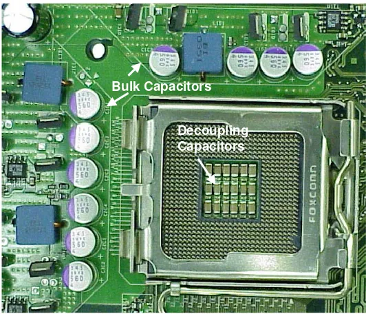
Bulk Capacitors Decoupling Capacitors
Figure 1.7 VRM components and CPU socket on the motherboard
1.4 Research motivations
Improving dynamic response without sacrificing power efficiency is one of the most popular topics in the filed of switching power supply design. Different approaches were proposed based on either the circuit topology or the control strategy.
approaches is using the circuits that only work during the transient, such as the active clamp [Li’06]. With these approaches, the switching DC-DC converter is designed only to supply the static current while the dynamic current is handled by the clamping circuits. Since the requirement of transient response on the switching DC-DC converter is reduced, it is possible to use relatively low switching frequency to achieve higher efficiency. In practical design, the power loss in the clamping circuits should be well limited so that the overall efficiency is not degraded too much by the clamping circuits. Compared with the control approaches, the topology approaches have more flexibility in design, but adding the extra circuits may increase design complexity, the cost and the size of the system.
achieve good dynamic response without sacrificing power efficiency. If the control of the variable frequency is implemented with linear circuits, the system can be well modeled and analyzed with simple linear models. Robustness of design can be achieved in the design. Besides, power efficiency in the light load condition can be dramatically improved by reducing the switching frequency. The control technique with variable frequency can cover both the light load condition and the heavy load condition and give smooth transition between them. On the contrary, in the typical constant frequency controls, a dedicated control for light load condition, such as burst mode control, pulse-skipping control, is designed in addition to the normal control mode for heavy load. The transition between the two controls is always headache in the design.
Load
current
Switching
pulses
Figure 1.8 Variable switching frequency changing with load current
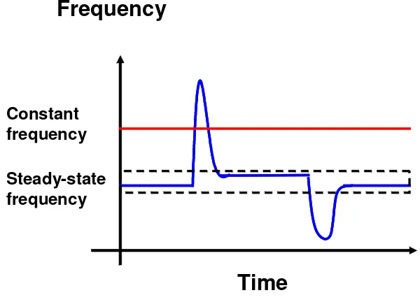
Frequency
Time
Steady-statefrequency Constant frequency
Figure 1.9 Plot of frequency versus time in variable frequency control
1.5 Outline of dissertation
Chapter 2 Current Mode Variable Frequency Control
2.1 Background and review of conventional PWM control
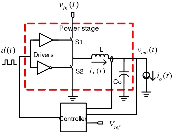
A DC-DC converter can be partitioned into two parts: the power stage and the controller. A single channel Buck converter is shown in Fig. 2.1 as an example. The power stage is a multiple-input single-output system. The system inputs are the driver signal d(t)and the input voltagevin(t), and the system output is the output voltagevout(t). The state of system can be represented by two state variables, the output voltagevout(t) and the inductor currentiL(t). The purpose of the control is to maintain the output voltage
constant and equal to the reference voltageVref.
Power stage
L
Co
)
(
t
d
)
(
t
v
in)
(
t
v
out)
(
t
i
Lref
V
)
(
t
i
oDrivers
Controller S1
S2
Figure 2.1 Block diagram of a DC-DC converter
Since the DC-DC converter is connected to the pre-regulated power supply or the battery,
the input voltage vin(t)can be modeled as a voltage source with certain output impedance.
switch S1 is conducting the current from the input source to the load; during off time the
synchronous rectifier S2 is conducting the free wheeling current in the inductor. If the
period of the pulse cycle,Ts, is constant, d(t)can be represented by the duty cycle or the
pulse width (or the on time ton):
s on s on
off on
on
f t T t t t
t
dutycycle = =
+
= (2.1)
If switching frequency is constant, the pulse width is modulated in the control. In this
dissertation, control with constant switching frequency is referred as the Pulse Width
Modulation (PWM) control. In fact, most of commercial switching DC-DC converters
are designed with the PWM control. Varieties of PWM control methods have been
developed. The implementation of the PWM control has standard design procedures
[Patel’85].
Existing PWM control methods can be categorized by signals used in the feedback:
voltage mode controls only use output voltage feedback; current mode controls use
feedback of both the output voltage and the current [Dixon’85]. Fig. 2.2 shows a simple
implementation of the voltage mode control, where the circuit that transfers the error
signalve(t) into the driver signal is the PWM modulator. For current mode controls,
many implementation methods have been developed. The current mode control methods
can be roughly categorized by implementations of current sensing: the Instantaneous
Current Mode control (ICM control), the Average Current Mode control (ACM control)
and the indirect current mode control. Specifically, the ICM control senses instantaneous
current waveforms in either the inductors or the switches. The examples of the ICM
control (or the current injection control), the valley current control, etc [Dixon’85]. An
implementation of the peak current control is shown in Fig. 2.3. The ACM control senses
averaged current information, which means AC ripples in the inductor current are
reduced by filtering and only low frequency components of the current signals are used
for control [Tang’93-2]. An example of ACM is the active droop control [Yao’03-2]
shown in Fig. 2.4. The indirect current mode control uses the current information in
alternative forms. For example, integration of the current is used in the charge control
[Tang’93-1]. Sometimes, sensing the current indirectly saves much effort in circuit
implementation. Each implementation approach of the current mode control has its own
advantages and limitations. Proper choice of the control depends on the specific
application. The control discussed in this dissertation falls into the first category, the
instantaneous current mode control.
L Co
)
(
t
d
)
(
t
v
in)
(
t
v
out)
(
t
i
L ref V)
(
t
i
o S1 S2 R S QRS Latch Comparator
Error amplifier Clock Ramp PWM Modulator
)
(
t
v
e Clock Ramp)
(
t
v
e)
(
t
d
Rc Rl e Sref
V
R
S Q
RS Latch Comparator
Error amplifier Clock
Ramp
v
e(
t
)
)
(
t
v
L iramp
t
v
e(
)
−
Clock
)
(
t
d
)
(
t
v
L i i R L Co)
(
t
d
)
(
t
v
in)
(
t
v
out)
(
t
i
Li
(
t
)
o S1 S2 Rc Rl e S n S
Figure 2.3 An implementation of peak current control
ref
V
RS Q
RS LatchComparator
Error amplifier Clock Ramp
)
(
t
v
L i i R)
(
t
v
e L Co)
(
t
d
)
(
t
v
in)
(
t
v
out)
(
t
i
Li
(
t
)
o S1
S2 Rc
Rl
Figure 2.4 An implementation of active droop control
Modeling and analysis of the control system in switching DC-DC converters is usually
done by small signal analysis in frequency domain [Ridley’88]. Since the system in
approximation is needed before the system can be simply modeled as a continuous linear
system. A useful method of approximation is averaging in which switching ripples are
omitted and only averaged signals are considered in the model. It should be noted that the
averaged model is accurate only if the interested frequency is much lower than the
switching frequency [Ridley’88]. With this assumption, the system is linearized and
characterized by the transfer functions. The system block diagram can be used to analyze
the feedback loops. Fig. 2.5 and Fig. 2.6 show the system block diagrams of the voltage
mode control and the peak current control system, respectively.
-Zo(s)
Gvd(s)
Gii(s)
Gid(s)
o
i
ˆ
d
ˆ
out
v
ˆ
L
i
ˆ
EA(s) Fm
Vref
-Zo(s)
Gvd(s)
Gii(s)
Gid(s)
o
i
ˆ
d
ˆ
out
v
ˆ
L
i
ˆ
EA(s) Fm
Ri
He(s)
Vref
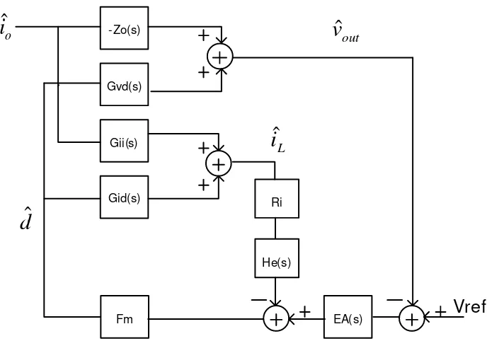
Figure 2.6 System block diagram of a DC-DC converter with peak current control
Here,Gvd(s),Gid(s) ,Gii(s)andZo(s) are transfer functions of the power stage. The
definitions and equations of these transfer functions in the Buck converter under
Continuous Conduction Mode (CCM) are listed as in Table 2.1. EA(s) is the transfer
function of the error amplifier. Fm and Riare small signal gains of the PWM modulator
and the current sensing gain, respectively. In Fig. 2.6, He(s)models the sampling effect
Table 2.1 Transfer function gains in small signal models o c l o o c in I out vd C R R Q LC s Q s C sR V d v G
o ( )
1 , 1 , 1 1 ˆ ˆ 0 0 2 0 0 + = = + + + = =
ω
ω
ω
ω
2 0 0 1 ˆ ˆ + + = =ω
ω
s Q s sC V d i G o in I L id o 2 0 0 2 1 1 1 1 1 ˆ ˆ + + + + = − =ω
ω
ω
ω
s Q s s Q s R i v Z l D o out o , ) ( 1 , 1 1 1 1 o l c c lo RC
R L Q
R R
LC = +
=
ω
ω
2 0 0 1 1 ˆ ˆ + + + = =ω
ω
s Q s C sR i iG c o
D o L ii
Voltage mode control Peak current control
L V V R S T S S
F n i in out
s n e m ) ( , ) ( 1 − = + = s e m T S F = 1
e
S : Slope of the ramp
π
π
ω
ω
ω
2 , , 1 ) ( 2 − = = + + ≈ z s n n z n e Q T s Q s s HWith the small signal model, important characteristics of the control system, such as open
loop gains and output impedance, can be calculated.
m vd
v s G s EA s F
T ( )= ( ) ( ) (2.2)
) ( )
( )
(s G s RF H s
Ti = id i m e (2.3)
) ( ) ( 1 ) ( ) ( 1 ) ( s H F R s G F s EA s G T T s T e m i id m vd i v + = +
) 1 , 0 ( , 1 1 ) 1 )( 1 ( ) 1 )( 1 ( ) ( 2 2 >> = + + ≈ + + + + + +
= i i
o c i i o c o c
oc T orT
T sC R T T T sC R Ls Ls sC R s
Z (2.5)
Here, Tv(s)and Ti(s)are the voltage loop gain and the current loop gain, respectively.
) (s
T is the overall voltage loop gain with current loop closed. Zoc(s)is the closed-loop
output impedance. In Equ. 2.5, the approximation is valid in voltage mode control (Ti =0)
and at frequency range whereTi >>1 in the current mode control. In the typical design
approaches, system stability and dynamic response is designed by choosing proper gains,
includingEA(s),Riand Fm. Bode plots can be used to evaluate system characteristics
[Erickson’01].
2.2 Design considerations of load transient response
In high current DC-DC converters, such as VRMs, transient response is extremely
important. The voltage spikes during load current transient must be limited within the
tolerance window. To understand the constraints of the transient response in the
converters, three major limiting factors are analyzed.
1. Switching frequency
Switching frequency determines the sampling rate in the PWM modulation. As illustrated
in Fig. 2.7, ve(t)is sampled every clock cycle. To avoid aliasing effects, the system
bandwidth must be less than half of the switching frequency. In real implementation,
large amount of noise exists at the frequency band close to the switching frequency.
Because of non-linearities in the circuit, the noise could be transferred to low frequency
improve system robustness under influence of the noise. It is common practice to design
the loop gain bandwidth less than one fifth of the switching frequency [Mitchell’01].
Furthermore, the switching frequency also affects system transient response by the action
delay effect that is not reflected in the small signal model [Wong’02-1]. If the transient
event occurs after the switch is turned off, the converter needs to wait until next
switching cycle to take any action. If the switching frequency is low, this delay could be
long enough to cause significant voltage drop during step-up transient of the load current.
Some design modifications were reported to improve transient response by introducing
duty cycle saturation in PWM modulation [Panov’01]. For example, by modifying the
PWM modulator, the duty cycle is changed to zero or maximum duty cycle immediately
after vout(t)or ve(t)is out of the preset boundaries. Because of nonlinear nature of this
design, system stability cannot be predicted by the developed linear models. Tuning of
the circuit parameters is necessary to guarantee system stability in all conditions.
)
(
t
v
e)
(
t
d
Figure 2.7 Sampling control signal with constant ramp signal
2. Output inductor
If all parasitic elements are ignored, the output filter is simplified as in Fig. 2.8. Voltage
variation during the load transient is determined by the charge unbalance in the output
capacitor [Wong’98]. From simplified current waveforms in Fig. 2.8, the voltage spike is
max 2 2 )] ( ) ( [ dt di C I C dt t i t i v L o o o o L out = − =
∆
∫
(2.6)The maximum slew rates of the inductor current for step up and step down are
determined by the input voltage, the output voltage and the inductance value:
L V V dt
di in out
up
L = −
max , , L V V dt
di out diode
down
L = +
max ,
(2.7)
Here, Vdiode ≈0.7Vis the voltage drop on the body diode of the synchronous rectifier.
Since the slew rate of the inductor current is limited by the inductance value, reducing
inductance helps improving system response to the load transient. The relation of the
inductance and the control bandwidth was analyzed in [Wong’02-2]. In practice, there are
more considerations on the inductor design. For instance, relatively large inductance is
sometimes needed to improve the power efficiency or to reduce the voltage ripple. For
the control design, letting the inductor currents slew with maximum slew rates during the
transient gives the best performance of transient response. In another words, faster
transient response can be obtained by saturating duty cycle during large load transient.
However, saturated control circuits may cause trouble in stabilizing the system.
)
(
t
i
o ) (t iL L Co up Ldt
di
down Ldt
di
) (t ioOutput filter Inductor current and load current
)
(
t
i
L3. Power delivery network
Power delivery network (PDN) is the physical network from the power stage of the
switching converter to the internal power bus of the load circuit [Ren’05-2]. Physical
connection between the VRM and the microprocessor is shown in Fig. 2.9. A circuit
model of PDN is shown in Fig.2.10. Because high current goes through PDN, the
parasitic inductance and resistance in PDN play important role during the current
transient. High frequency impedance made by the PDN between the power supply and
the load circuits could cause excessive voltage variations or even resonance on the
internal voltage bus excited by high frequency current transients [Muhtaroglu’04].
Comprehensive design efforts are needed to maintain low impedance over required
frequency range, including power supply design, motherboard design, chip package
design and on-chip power bus design [Ji’05] [Arabi’04]. For power supply design, the
issue is usually reduced to designing the control system with proper output capacitors and
optimizing layout of the power path on the motherboard. To simplify the power supply
design, the load is usually modeled as a dynamic current source instead of the complex
PDN. The effect of PDN is represented by the slew rate of the current source. For
example, a current source with slew rate of 100 A/µs connected to the decoupling
Socket Processor
OLGA
Oscon Socket
Processor
OLGA
Oscon
Processor
OLGA
Oscon Oscon
Figure 2.9 Simplified connection between VRM and CPU on motherboard
Packaging cap
Cap on die Packaging
cap
Cap on die Cap on
die
Bulk Cap
around the socketDecoupling capBulk Cap
around the socketDecoupling cap Decoupling cap in the cavity Decoupling cap inthe cavity Decoupling cap in
the cavity
Figure 2.10 A circuit model of power delivery network between VRM and CPU
2.3 Design with adaptive voltage positioning
Adaptive Voltage Positioning (AVP) is a design approach that helps to improve load
transient response of the switching DC-DC converters and reduce the amount of output
capacitors required to meet the specifications [Waizman’01]. With AVP design, the
output voltage varies with the load current as shown in Fig. 2.11. Compared with
non-AVP design, the allowed voltage variation for full swing load transient is doubled with
AVP design. The effective output impedance in ideal AVP design behaves like a constant
resistance over certain frequency range. Fig. 2.12 is the load line at steady state. The
slope of the load line is referred as the load line resistance or the droop resistanceRdroop.
voltage gets lower, the trend of the droop resistance is getting smaller. The output voltage
at steady state can be expressed as:
droop o ref
out V I R
V = − (2.8)
iO iO
∆ ∆ ∆ ∆Vp-p
W/O AVP ∆∆∆∆Vp-p
W/O AVP VO
VO
W/ AVP
0.5·∆∆∆∆Vp-p W/ AVP
0.5·∆∆∆∆Vp-p 0.5·∆∆∆∆Vp-p
Figure 2.11 Transient voltage waveforms w/ and w/o AVP design
Load current
Output voltage
Vref
Figure 2.12 The load line of the output voltage
Implementation of AVP design is studied in [Yao’04]. The principle of AVP design is to
of the PDN is shown in Fig. 2.13. Usually, large volume electrolytic capacitors are used
as the bulk capacitors, and small volume Multi-Layer Ceramic Capacitors (MLCC) are
used for the high frequency decoupling capacitors. The impedance of the bulk
capacitorsZCband the impedance of the decoupling capacitorsZCeare plotted in Fig. 2.14.
Because of Co >>Ce, the PDN impedance is dominated byZCbat low frequency. The
PDN impedance at high frequency is determined by bothZCeand other components in
PDN. With feedback control, the closed loop output impedance Zoc is regulated at
frequency below the bandwidth. As shown in Fig. 2.14, a good approach to achieve
flat Zoc is to design the control bandwidth of T2 at
o c ESR C R 1 =
ω
and Rc =Rdroop .According to (2.5), the transfer function of T2should be designed as:
o C ESR C sR s
T2 =
ω
= 1 (2.9)It should be noted that, in current mode control,Ti >>1 is required within bandwidth of
2
T to satisfy approximation in (2.5).
o
C
C
ec
R
cL
2 cR
2 cL
L
Bulk Capacitors Decoupling
Capacitors
p
L
R
p Othercomponents in PDN
o c ESR
C R
1 =
ω Cb
Z
Z
Ceoc
Z
s
T
2=
ω
ESRESL
ω
droop
C
R
R
=
Frequency in logarithm Amplitude
in dB
Figure 2.14 Plots of impedance for AVP design
2.4 Control with variable switching frequency
If the switching frequency is no longer constant in control, one more variable is
controllable than in the constant frequency control, which gives more flexibility to the
control design. The control method with variable switching frequency is sometimes
referred as Pulse Frequency Modulation (PFM) control. The implementation of variable
frequency control can be either single-edge or double-edge. In the single-edge control,
either on time or off time is modulated while the other is kept unchanged. The examples
of the single-edge variable frequency control are on-time control and
constant-off-time control [Ridley’90]. In the double-edge control, both on time and off time are
modulated in control. The examples of double-edge variable frequency control include
hysteretic voltage control [Abu-Qahouq’04], sliding mode control [Giral’00] and
2.4.1 Constant on time control
Choosing single-edge control or double-edge control is tradeoff between control
flexibility and control complexity. For VRM applications, constant on time control has
several advantages in practical design.
First, the input voltage of VRMs is in the range of 12 V to 20 V, and output voltage in the
range of 0.5 V to 2 V. High input-voltage-to-output-voltage ratio indicates that the duty
cycle is small and the on time is short at steady state. The on time of some applications
could be as low as 50 ns. In circuits design, the minimum controllable time is limited by
delays in the drivers and other control circuits. It is not practical to modulate the on time
when the on time is close to the minimum controllable time. Besides, the current sensing
circuits have limited bandwidth, usually below 10 MHz. It is difficult to sense the
instantaneous current waveforms within such short on time. However, the off time is ten
times longer than the on time. If the off time is modulated, it is much easier to implement
the control circuits and current sensing circuits. Since high frequency switching noise has
been well damped during off period, the control robustness to noise can be significantly
improved with off time modulation. Secondly, the system reliability is enhanced with
fixed on time. The duration of the on time determines the amount of energy transferred
from the input voltage source to the load in each cycle. By fixing the on time, limited
energy flows into the converter in each cycle, which helps protecting the load and the
power switches when system malfunction or overloading happens.
2.4.2 Frequency regulation at steady state
In DC-DC converter design, it is beneficial to keep the steady-state switching frequency
converter. For constant-on-time control under CCM, the switching frequency at steady
state varies with the input voltage and the output voltage. Since the input voltage and the
output voltage are varying slowly, it is possible to regulate the steady-state switching
frequency by adjusting on time accordingly. If all power loss is ignored, the steady-state
switching frequency of the Buck converter under CCM is:
on in ref
on in out s
t V V t V V
f ≈ 1 = 1 (2.10)
If tonis designed linearly proportional to
in ref
V V
, the dependency of fson the input voltage
and output voltage can be removed. The value of fscan be adjusted by changing the
2.5 Proposed control scheme with variable switching frequency
2.5.1 System architecture
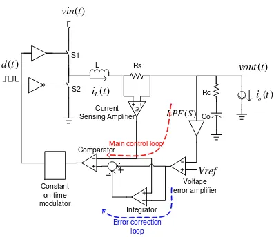
The proposed control scheme employs constant-on-time current-mode control with novel
system architecture illustrated in Fig. 2.15. HereRsis the current sensing gain; LPF(s)is
the transfer function of the low pass filter. The current sensing amplifier and the voltage
error amplifier have constant gain up to their bandwidths. Because of the 3-dB
bandwidths of the amplifiers are designed much higher than the system bandwidth, the
gains of the current sensing amplifier and the voltage error amplifier are simplified as the
constants: Aiand Av, respectively.
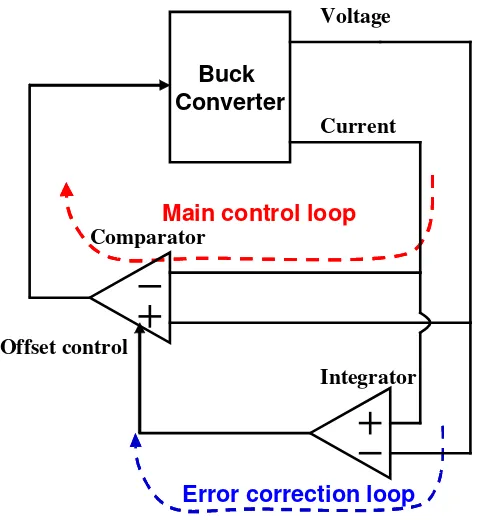
To understand the control system, the system is divided into a main control loop and an
error correction loop as shown in Fig. 2.16. In the main feedback loop, the driver signal
) (t
d is generated by comparing the outputs of the current sensing amplifier and the
voltage error amplifier. Because of high bandwidth in this loop, fast transient response
could be achieved. Besides, the switching frequency can instantaneously change during
the transient. The transient response is no longer limited by the steady-state switching
frequency. Lower steady-state switching frequency could be designed to improve the
efficiency. However, the output voltage accuracy is affected by the current ripple, offset
of the comparator, and delays in the loop. The additional error correction loop is added to
remove the static error. With the integrator in the error correction loop, the error is
amplified and injected back into the main feedback loop. A small offset added to the
comparator compensates the static error introduced in the main feedback loop. Since the
high frequency load transient is mainly related to the main feedback loop, the frequency
system stability. The frequency characteristics of the two loops are illustrated in Fig.
2.17.
Vref
Comparator L
Co
)
(
t
d
)
(
t
vin
)
(
t
vout
)
(
t
i
Li
(
t
)
o
S1
S2 Rc
A
i
Constant on time modulator
Integrator Rs
Current Sensing Amplifier
Voltage error amplifier
)
(
S
LPF
Error correction loop
Main control loop
Figure 2.15 System schematics with proposed control scheme
Therefore, the proposed control scheme combines the advantages from traditional current
mode control and constant-on-time variable frequency control to provide good tradeoff
between transient response and steady state performance. In the proposed control
architecture, the traditional compensator is replaced by several simple blocks, such as the
low pass filter and the integrator, which simplifies the system design. Furthermore, the
proposed control scheme provides a good approach to implement AVP design, as
Buck Converter
Voltage
Current
Comparator
Main control loop
Integrator Offset control
Error correction loop
Figure 2.16 Simplified diagram showing two control loops
f
gain
Error correction loop
Main control loop
Figure 2.17 Frequency characteristics of the two control loops
2.5.2 AVP design
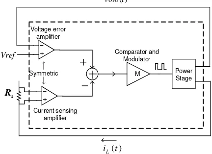
In Fig. 2.18, the simplified control system is drawn resembling a fully differential
amplifier in a closed-loop configuration. The voltage error amplifier and the current
sensing amplifier are equivalent to two input stages with finite gains. Combination of the
comparator, the modulator and the power stage behaves like an output stage with high
systematic offset. Therefore, the differential error between the two inputs of the output
stage is reduced to zero in average by the high gain. Since the outputs of the two input
stages are equal in the average, the following equation is obtained:
i s L v out
ref
v
A
i
R
A
V
−
>
=<
>
<
(2.11)Hence: v i s L ref out A A R i V
v >= −< >
< (2.12)
Compared with (2.8),
v i s droop A A R
R = (2.13)
It is noticed that the droop resistance is determined byRsand a ratio of two gains,
v i
A A
.
This arrangement has advantages to implement accurateRdroopwith integrated circuits. As
discussed in Chapter 4, the gain is determined by the on-chip components, such as the
resistors. The ratio of the gains is determined by the size ratio of these components. If
circuit structures of the two amplifiers are symmetric and good layout matching is
achieved, it is possible to cancel the gain variations from process variations and
temperature drifting. Although the droop resistance is influenced by tolerance of the
sensing gainRs, (2.13) implies that the tolerance of Rs can be simply compensated by
tuning the gain of one of the amplifiers. By designing variable gain circuits, the droop
resistance can be adjusted with high precision. Moreover, it is possible to reduce the
value of Rs to save power loss in the current sensing circuits by designing higher gain
M
Power
Stage
Voltage error
amplifier
Current sensing
amplifier
Comparator and
Modulator
)
(
t
i
L)
(
t
vout
Vref
s
R
Symmetric
Figure 2.18 Simplified system block diagram for AVP design
2.5.3 Small signal analysis
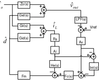
The small signal model for the proposed control architecture is shown in Fig. 2.19.
Here, Fc(s) is added to model the phase lead effect in the constant-on-time control
[Ridley’90], andINT(s)is the gain of the integrator in the error correction loop.
2
'
)
( sDTs
c s e
F = (2.14)
s s INT =
ω
i)
-Zo(s) Gvd(s) Gii(s) Gid(s) o
i
ˆ
d
ˆ
outv
ˆ
Li
ˆ
Fc(s) Fm Rs He(s) Ai LPF(s) Av Int(s) VrefFigure 2.19 Small signal model of proposed control scheme
From the developed model, the overall voltage loop gain Tcan be derived:
) ( ) ( 1 )) ( 1 )( ( 1 ) ( 2
1 G F R AH s G F R AF INT s A F F G s INT s LPF T T T s T c i s m id e i s m id v m c vd i i v + + + = + +
= (2.16)
The voltage loop gain, Tv, and the two current loop gains, Ti1andTi2are defined as
followings:
v m c vd
v LPF s INT s G F F A
T = ( )(1+ ( )) (2.17)
) ( 1 G F R AH s
Ti = id m s i e (2.18)
) ( 2 G F R AF INT s
Ti = id m s i c (2.19)
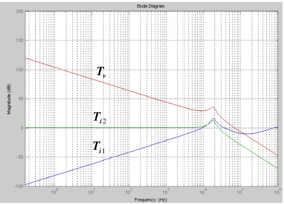
With typical design parameters, the magnitudes of two current loop gains are relatively
v T 2 i T 1 i T
Figure 2.20 Plot of the voltage loop gain and the current loop gains
At low frequency, the overall loop gain Tcan be approximated as:
v m vd v m c
vdF F A LPF s INT s G F A
G s INT s LPF s
T( )≈ ( )(1+ ( )) ≈ ( ) ( ) (2.20)
By substitutingGvdfrom Table 2.1 and (2.15), T is further simplified at low frequency
where
ω
<ω
0:s A F C sR V s LPF s Q s s A F C sR V s LPF s
T i in c o m v ( ) i in(1 c o) m v
) 1 ( ) 1 ( ) ( ) ( 2 0 2 0 + ≈ + + + ≈
ω
ω
ω
ω
(2.21)From the discussion in Section 2.3, the ideal loop gain in AVP design is
o cC
sR T = 1 .
In (2.21), the ideal loop gain can be obtained by choosing:
s C R s LPF o c + = 1 1 )
( (2.22)
and v m in o c i A F V C R 1 =
ω . (2.23)
Since FmandAv are the parameters that are related to the circuits inside the controller chip, it is
The modulation gain of the constant-on-time control is approximated as: s out i s s f m T L V A R D T S D
F = ≈ (2.24) [Ridley’90]
Hence, the value of
ω
ican be calculated from all external parameters:L C R T R DL V C R T V R o c s droop in o c s out droop
i = ≈
ω
(2.25)Amplitude (dB)
Frequency (Hz)
Fs=300 KHz, Vin=12 V, Vout = 1V, L=150nH, Co=0.5mF, Rc=2mΩΩΩΩ
ideal T
Designed T
Phase (degree)
Frequency (Hz)
Designed T w/o phase lead ideal T
Designed T w/ phase lead
Figure 2.21 Bode plot of open loop gains
With the design guidelines in (2.22) and (2.25), implementation of control loop is
simplified to design a first-order low pass filter and an integration capacitor. Once the
parameters, such asRdroop, Ts, L, are decided in design, output capacitanceCo can be
parameters. Fig. 2.21 shows an example of designed loop gain. It is noticed that the phase
margin is significantly boosted by the phase leading effect in the constant-on-time
control. The designed loop gain is very close to the ideal loop gain.
At the high frequency range that is close or beyond half of the steady state switching
frequency, the assumption of the small signal model is no longer valid. Furthermore, the
small signal analysis presented above assumes the switching frequency is constant, which
is not accurate to predict large signal transient. As shown in Fig. 2.22, the switching
frequency is significantly changed when large perturbation is applied during large load
transient.
(a)
(b)
1 i ∆
2 i ∆ L
i
ref
i
L
i
ref
i
Figure 2.22 Current transient waveforms under small and larger perturbations
Therefore, a new model is used to predict the system response with large signal transient.
The assumption of the model is that the inductor current will follow the envelop
generated by the voltage error amplifier, and the difference between the average value
and bottom envelop value of the inductor current is negligible. This assumption is
maximum or minimum boundaries during the transient), and the perturbation amplitude is
much larger than the ripple of the inductor current. Once the assumption is satisfied, the
inductor current is simplified as a voltage-controlled current source with the gain of
droop
R 1 −
, as shown in Fig. 2.23. The output impedance can be derived as:
droop o c o c o o oc R s LPF sC R sC R i v Z ) ( ) 1 ( 1 1 ˆ ˆ + + + = −
= (2.26)
o c
sC
R + 1 out
v
ˆ
oi
ˆ
L
i
ˆ
LPF
(
s
)
droop
R
1
−
Figure 2.23 Simplified feedback loop to analyze transient response
By substituting (2.22) and assuming Rdroop =Rc, the output impedance in (2.26) is
simplified as Zoc =Rdroop. From the new model it is concluded that, given the assumption
is satisfied, the system can maintain the output characteristics as required for large load
transient. The prediction of transient response by the model is verified by comparing
circuit simulation results and model simulation results at the transient, as shown in Fig.
Output voltage
Output voltage
Time
Time
Circuit simulation
model simulation
Figure 2.24 Comparison of results of circuit simulation and model simulation at transient
2.5.4 Comparison with peak current control
A case study was performed to compare the performance of the proposed control scheme
and the traditional peak current control. Two control systems were designed with the
same parameters listed in Table. 2.2:
Table 2.2 Parameters for control system design
Input voltage 12 V
Output voltage 1 V
Steady-state switching frequency 300 KHz
Inductor 150 nH
Maximum load current 20 A
Current sensing gain Rs 2 mΩ
Lumped ESR of output capacitors Rc 2 mΩ
The simulation models were built with Simulink in Matlab, as shown in Fig. 2.25 and
2.26.
Vi1
Ve1
Figure 2.25 Simulation diagram for proposed control
Vi2
Ve2
Figure 2.26 Simulation diagram for peak current control
Here, Ai and Avare modeled as the unit gain amplifiers with 3-dB bandwidth at 1 MHz:
6 10 28 . 6 / 1 1 ) ( ) ( × + = = s s A s
Ai v (2.27)
The low pass filter LPF and the integrator INT in Fig. 2.23 are designed as followings:
002 . 0 1 1 1 1 ) ( × + = + = o o
cC sC
sR s
s s INT 3 10 )
( = (2.29)
According to [Yao’04], the compensator for peak current control,Gc, is designed as:
002 . 0 1 10 4 . 9 1 1 1 ) ( 5 × + × + = + + = o o c s c s c sC s C sR f s R R s
G
π
(2.30)As non-idealities in the circuits, 10 mV offset voltage and 10 ns delay time were added to
the modulators in both systems.
The systems were simulated with the output capacitanceCoas a variable. In Fig. 2.27, the
waveforms show that both systems have stable switching with output capacitance equal
to 1 mF. However, the system with the peak current control has apparently larger voltage
error at steady state than the system with the proposed control. The DC error in the peak
current control system is caused by low DC gain in the feedback loop.
Output voltages
Inductor currents
Proposed control Peak current control
load current
DC error
Figure 2.27 Simulation waveforms with output capacitance of 1 mF
The internal control signals, i.e. outputs of current sensing amplifiers and error
amplifiers, are plotted in Fig. 2.28. It is noticed that the ripples on Ve2 have larger
amplitude than that on Ve1. The larger ripples on the control signal make the system with
peak current control (Equ. 2.30) is designed with one zero added at half of the switching
frequency, less attenuation is resulted for high frequency noise. Since in this design
approach [Yao’04] the zero is intentionally added to help system stability by increasing
phase lead in the loop, high bandwidth is not adequate for poor noise immunity.
Vi1
Ve1
Vi2 Ve2
Proposed control
Peak current control
Figure 2.28 Internal control signals in two systems (Co=1mF)
The value of output capacitance was further reduced to test the system performance at
higher frequency. With output capacitance equal to 0.4 mF, the results in Fig. 2.29 show
that the system with the peak current control was no longer stable. However, the system
with the proposed control is still stable and shows good regulation and load transient
response.
Output voltages
Inductor current
Proposed control Peak current control
Inductor currents load current