ISSN(Online): 2320-9801
ISSN (Print): 2320-9798
International Journal of Innovative Research in Computer
and Communication Engineering
(An ISO 3297: 2007 Certified Organization)
Vol. 3, Issue 8, August 2015
Low Power Conditional Pulse Control Flip
Flop Using Signal Feed Through Scheme
Resham Singh1, Bal Krishan2, Naveen Sigroha3
M.Tech Scholar (VLSI Design), Department of Electronics Engineering, YMCA University of Science and
Technology, Faridabad, Haryana, India1,3
Assistant Professor, Department of Electronics Engineering, YMCA University of Science and Technology, Faridabad,
Haryana, India2
ABSTRACT: In the present work, Low Power Conditional Pulse Control Flip-Flop using Signal Feed through scheme
is proposed. The proposed design removes the long discharging path problem with intermediate nodes using the pulse generation control (which facilitates a faster discharge operation). Transmission gate and three inverters are used to control the clock circuit to reduce the power dissipation along the critical path. As a result, very low power dissipation occurs when there is no switching. Tanner EDA tool 14.1 is used for the simulation purposes. All simulation results are based on using CMOS 90-nm technology at 500MHz clock frequency. Its maximum power saving compared to PT-FF with Pulse Enhancement Scheme FF design[1][2] is up to 26.84% and 14.72% than PT-FF with Pulse Enhancement Scheme FF design [1].
KEYWORDS: Flip-Flop; Low power; Signal feed through scheme; Conditional pulse; Transmission gate circuit;
Sequential circuits; Lower power dissipation.
I. INTRODUCTION
Flip-flops (FFs) are the main storage used in digital circuits. In particular, digital designs nowadays often adopt intensive pipelining techniques and employ many FF-affluent modules such as register files, FIFO, counters and shift registers [1], [2]. The performance of the Flip-Flop is an important element to determine the performance of the whole circuit. FFs are not only responsible for the functionality, correct timing and performance of the entire chip, but also these and other clock systems, which consist of the clock distribution network and sequential elements (latches), consume a significant portion (around 45-50%) of the total power of the circuit in a Very Large Scale Integration (VLSI) systems. Power dissipation of FFs is determined by factors such as clock frequency, power supply, switching activity, load capacitance, short circuit power and leakage power [3]. For the improvements in the FF design, delay, power and area of the FFs should be smaller.
There are mainly three types of flip-flop circuits used in digital systems, first is the pulse triggered based, second is the transmission gate based and third is the master-slave based FFs. From all these FFs, pulse triggered based FFs are mostly preferred due to their single latch structure and better power efficiency. These pulse triggered FFs are of two types, one is implicit type (pulse generator is the part of latch) and other is explicit type (pulse generator and latch are separate) FFs [4]. In these FFs, pulse is generated by the clock circuitry at the rising or falling edge of the clock. So, circuit changes its behavior in accordance with the generated pulse. Some other approaches are also used to design the FFs such as semi dynamic, sense amplifier based and hybrid latch based [5]-[12]. In the present work, alow power conditional pulse control flip-flop using signal feed through scheme is proposed.
II. PREVIOUS FF DESIGNS
ISSN(Online): 2320-9801
ISSN (Print): 2320-9798
International Journal of Innovative Research in Computer
and Communication Engineering
(An ISO 3297: 2007 Certified Organization)
Vol. 3, Issue 8, August 2015
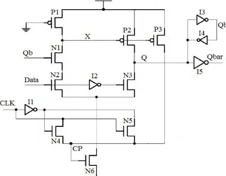
most of the time. After the rising edge of the clock, the clock delay inverter drives output node back to zero but with little delay. This generates the clock pulse and the generated clock pulse is taller in height, which enhances the pull-down strength of lower N6 transistor which is responsible for the discharging. After the clock has reached to logic 1, then lower N6 is turn off due to no clock pulse.
Fig. 1. (a) PT-FF with Pulse Enhancement Scheme
Then voltage level of node X rises and turns off upper transistor P3 eventually. With the help of extra P3 transistor, the width of the generated discharging pulse is stretched out. This creates a pulse with sufficient width for correct data requirement, a bulky delay inverter design, which comprises most of the power consumption in pulse generation logic, is no longer required. It should be noted that this conditional pulse enhancement technique takes effects only when FF output is subject to a data change from 0 to 1. This leads to low power consumption in the FF circuit. This also reduces the leakage power due to shrunken transistors in the discharging path.
III. PROPOSED FF DESIGN
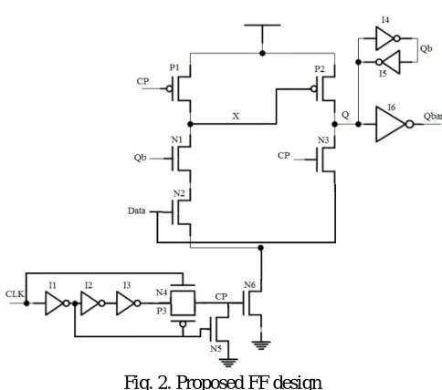
Fig. 2 shows proposed FF design circuit. In proposed design, clock is controlled by the transmission gates (parallel combination of the NMOS and PMOS) which lower the power dissipation when there is no switching. It results in low leakage power. This design is the combination of TSPC and transmission gate structure to implement low power and faster D-FF. This uses conditional discharge approach for reducing internal switching activity [6]-[10]. In the new clock pulse generator, three inverters, one transmission gate and a NMOS are responsible for the clock pulse generation at the rising edge of the clock. When the clock is “0” then output of the 1st and 3rd inverter is “1”. So due to this, transmission gate transistors N4 and P3 are OFF and transistor N5 is ON that makes node CP is “0”. And when the
clock is “1” then output of the 1st and 3rd inverter is “0” that makes transmission gate ON for the third inverter output
“0” to reach to node CP. Here, clock pulse is generated only in one case, when clock goes from “0” to “1” means at the
rising edge of the clock. When clock is “0” then 3rd inverter output is “1” and transmission gate is OFF, but when clock
goes to “1” then transmission gate becomes ON that transfer the output of 3rd inverter “1” to node CP which becomes
ISSN(Online): 2320-9801
ISSN (Print): 2320-9798
International Journal of Innovative Research in Computer
and Communication Engineering
(An ISO 3297: 2007 Certified Organization)
Vol. 3, Issue 8, August 2015
Fig. 2. Proposed FF design
When input Data becomes “0” and assuming Q is “1” from previous case then with the clock pulse, transistor N3 becomes ON which discharge the output Q through input Data source rapidly. It makes discharging of the output faster. Due to its discharging controlled by transmission gates and signal feed through technique, this proposed FF has very low leakage power in standby mode and low average power dissipation in active mode. Here, inverters I4 and I5 are used to maintain the level of output. Inverter I6 is used to get Qbar (inverted output of Q) at the same time.
IV. SIMULATION RESULTS
Simulations are performed using 90nm CMOS process technology and assume clock frequency as 500MHz at 1V power supply. Here, each FF is individually optimized for the PDP (Power and D-to-Q delay product). For the rise and fall time delays, buffers are used at the input of Data and Clock. Here, buffers are used to create a delay 100ps in both the signals. A load capacitance of 20fF has been assumed at the output of all FFs. All designs are optimized for the power-delay product. Fig. 3 shows the setup of the simulation model. Since width of the clock pulse is the crucial part for the circuit operation and power consumption, so we first designed the explicit clock pulse generator for proper functioning.
ISSN(Online): 2320-9801
ISSN (Print): 2320-9798
International Journal of Innovative Research in Computer
and Communication Engineering
(An ISO 3297: 2007 Certified Organization)
Vol. 3, Issue 8, August 2015
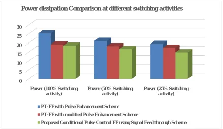
TABLE I. Comparison of different parameters of different FFs
Flip-Flops PT-FF with Pulse
Enhancement Scheme
PT-FF with modified Pulse Enhancement
Scheme
Proposed Conditional Pulse Control FF using
Signal Feed through Scheme
No. of Transistors 19 19 21
D-to-Q delay 148.45 124.53 108.26
Power (100% Switching activity) 25.18 19.15 18.42
Power (50% Switching activity) 21.09 18.13 16.58
Power (25% Switching activity) 19.43 17.25 14.71
PDP (50% Switching activity) 3.13 2.25 1.79
Table I shows comparison of different FFs. Fig. 4 shows the graph of power dissipation at different switching activities. It is clear from Fig. 4 that proposed design consumes minimum power at 100%, 50% and 25% activity compared to other designs.
Fig. 4. Graph of power dissipation at different switching activities.
V. CONCLUSION
A low power conditional pulse control flip-flop based on signal feed through scheme is proposed in the present work. Proposed design is simulated using CMOS 90nm process technology. Obtained results show that proposed design has low D-to-Q delay compared to the other designs. Also the proposed design dissipates lesser leakage power compared to the other designs. In addition, the average power consumption of the proposed design is 26.84% lesser than PT-FF with Pulse Enhancement SchemeFF design and 14.72% than PT-FF with Pulse Enhancement Scheme FF design.
0 5 10 15 20 25 30
Power (100% Switching activity)
Power (50% Switching activity)
Power (25% Switching activity)
Power dissipation Comparison at different switching activities
PT-FF with Pulse Enhancement Scheme
PT-FF with modified Pulse Enhancement Scheme
ISSN(Online): 2320-9801
ISSN (Print): 2320-9798
International Journal of Innovative Research in Computer
and Communication Engineering
(An ISO 3297: 2007 Certified Organization)
Vol. 3, Issue 8, August 2015
REFERENCES
1. R. Singh, N.Sigroha, R. Rohila, B. Krishan, “Low power pulse triggered flip flop design with modified conditional pulse enhancement scheme,” International Journal for Scientific Research & Development, vol. 3, issue 01, ISSN (online): 2321-0613, 2015.
2. Y.T. Hwang, J.F. Lin, and M.H. Sheu, “Low-power pulse-triggered flip- flop design with conditional pulse-enhancement scheme” IEEE Transaction on Very Large Scale Integration (VLSI) Systems, vol. 20, no. 2, pp. 361-366, Feb 2012.
3. P. Zhao, J. McNeely, W. Kuang, N. Wang, and Z. Wang, “Design of sequential elements for low power clocking system,” IEEE Transactions on Very Large Scale Integration (VLSI) Systems, vol. 19, no. 5, pp. 914-918, May 2011.
4. J.F. Lin, “Low-power pulse-triggered flip-flop design based on a signal feed-through scheme” IEEE Transaction on Very Large Scale Integration (VLSI) Systems, vol. 22, no. 1, pp. 181-185, Jan 2014.
5. Stojanovic and V. Oklobdzija, “Comparative analysis of master-slave latches and flip-flops for high-performance and low-power systems,” IEEE J. Solid-State Circuits, vol. 34, no. 4, pp. 536–548, Apr. 1999.
6. S. H. Rasouli, A. Khademzadeh, A. Afzali-Kusha, and M. Nourani, “Low power single and double-edge-triggered flip-flops for high speed applications,” IEEE Proc. Circuits Devices Syst., vol. 152, no. 2, pp. 118–122, Apr. 2005.
7. P. Zhao, T. Darwish, and M. Bayoumi, “High-performance and low-power conditional discharge flip-flop ,” IEEE Transaction on Very Large Scale Integration (VLSI) Systems, vol. 12, no. 5, pp. 477-484, May 2004.
8. H. Kawaguchi and T. Sakurai, “A reduced clock-swing flip-flop (RCSFF) for 63% power reduction,” IEEE J. Solid-State Circuits, vol. 33, no. 5, pp. 807– 811, May 1998.
9. K. Chen, “A 77% energy saving 22-transistor single phase clocking D-flip-flop with adoptive-coupling configuration in 40 nm CMOS,” in Proc. IEEE Int. Solid-State Circuits Conf., Nov. 2011, pp. 338–339.
10. E. Consoli, M. Alioto, G. Palumbo, and J. Rabaey, “Conditional pushpull pulsed latch with 726 fJops energy delay product in 65 nm CMOS,” in Proc. IEEE Int. Solid-State Circuits Conf., Feb. 2012, pp. 482–483.
11. H. Partovi, R. Burd, U. Salim, F.Weber, L. DiGregorio, and D. Draper, “Flow-through latch and edge-triggered flip-flop hybrid elements,” in Proc. IEEE Int. Solid-State Circuits Conf., Feb. 1996, pp. 138–139.