Terahertz Graphene-Based Reconfigurable Patch Antenna
Mohamed K. Azizi1, *, Mohamed A. Ksiksi1, Hosni Ajlani2, and Ali Gharsallah1
Abstract—The radiation properties of a copper-patch antenna designed for resonating at the frequency of 0.7 THz, which is used in aerospace applications, is presented. These properties are then compared to those of a graphene-patch antenna presenting the same dimensions. We show how the use of graphene, as a tunable material, allows to dynamically modify the frequency of operation of the antenna as well as its radiation pattern. Our results show that the return loss peak reaches−29 dB, at the operating frequency, which is almost twice the value obtained with the copper patch. This increase in the return loss peak is also accompanied by an improvement in the gain of the antenna from 5.73 dB in the case of the copper patch to 7.16 dB in the case of graphene. We focus our interest on how the reconfigurable radiation properties of the graphene-patch antenna are directly related to the graphene surface conductivity.
1. INTRODUCTION
Electromagnetic waves are the most powerful tool to study the universe. This tool allows us to study particles of size from infinitely large to infinitely small. The wide spectrum of the electromagnetic spectrum makes it possible to carry out numerous applications such as the study of galaxies in astronomy, also the study of nuclear physics. Among different wavelength ranges of the electromagnetic spectrum, the scientific community is studying the terahertz frequencies very intensely [1–4]. For about twenty years, the terahertz (THz) frequency range has become more readily available with the development of ultra-fast lasers capable of generating pulses lasting a few tens of femtoseconds [5]. Previously, these THz frequencies were only accessible by synchrotrons [6], free-electron lasers [7] and molecular gas lasers [8]. The THz frequencies are between the frequencies 100 GHz and 10000 GHz, and they are located between infrared waves and microwaves. To better define the frequency range THz, the duration of an electromagnetic cycle at 1 THz is 1 ps; the wavelength is 300µm; the energy is 4.1 meV; the temperature is 48◦K. The reasons that the scientific community is intensifying research into the development of generation techniques, detection techniques and, of course, THz applications are that THz waves have unique characteristics for probing matter since they can penetrate non-metallic materials such as plastics, paper, wood, gases, textiles as well as organic materials. These materials are transparent to the THz waves since they are devoid of free loads. On the other hand, these waves of low energies are called non-ionizing (Unlike X-rays) and do not damage the samples. Also, many molecules have distinct imprints in the THz spectrum. In fact, many molecules such as water, DNA, drugs or TNT absorb the THz waves because the rotational and vibrational energy of these molecules corresponds to the energy of a THz photon [9]. Among applications using THz waves, we can mention applications in security [10], imaging [11], and biomedical applications [12].
A reconfigurable antenna is an antenna of which at least one of the characteristics is modifiable after its manufacture, by application of a command. There are many ways of classifying reconfigurable antennas. This can be done, for example, depending on the physical property that makes them
Received 14 August 2017, Accepted 11 October 2017, Scheduled 25 October 2017
* Corresponding author: Mohamed Karim Azizi ([email protected]).
1 Unit of research Circuits and Electronics Systems High Frequency, Faculty of Science, University El Manar, Tunis, Tunisia. 2Unit
reconfigurable (modification of current lines, modification of dielectric/diamagnetic properties of antenna elements, geometrical deformation), depending on the type of reconfigurable components used (diodes, Transistors, MEMS. . . ) or depending on their geometrical structure (type of reconfigurable structure, a priori geometry of the antenna. . . ). The reconfiguration of the antenna can be achieved by various approaches. Some techniques have recourse to localized active components which make it possible to modify quasi-punctual lines of current or impedance [13], and some rely on mechanical alteration of the structure constituting the antenna [14], while others use substrates with tunable characteristics [15]. Some approaches rely on the reconfigurability of the power supply networks [16] or properly excite the antenna arrays [17]. With the progress of microelectronics, the use of actuated switches electrically and varactors has offered new means to obtain reconfigurable structures. Indeed, inserted into the structure of the antenna, they make it possible to modify its effective electrical length, to modify the size and/or the shape of the radiating element, to make short circuits or slots which can be switched, to add spurious elements, and this in a controlled manner. Its modifications are carried out discretely (switching) or continuously (tunability). However, the use of these components generates considerable congestion and additional manufacturing costs.
Other approaches to modify the electromagnetic properties of an antenna without the use of additional components include the use of “agile” or “intelligent” materials, whose dielectric properties (permittivity and/or permeability) can be modified via an external control (effect of an electric and/or magnetic field, respectively). They are mostly used as patch or substrate layer on which the antennas are made. Among these materials, graphene [18] is the most remarkable. This material with exceptional optical [19, 20] and electronic properties [21] has the advantage of seeing these properties adjustable thanks to the application of an external voltage [22–24].
In this paper, we study a rectangular graphene-microstrip-patch antenna. We compare the return loss curves and the polar plot of far-field gain of a conventional cupper-patch antenna with those of a graphene-patch antenna. Our results show how an applied external electric fields to the graphene patch allow the control and the adjustment of the resonance frequency of the studied antenna. We focus our interest on the resonating frequency of 0.7 THz which is used in aerospace applications.
2. THEORY
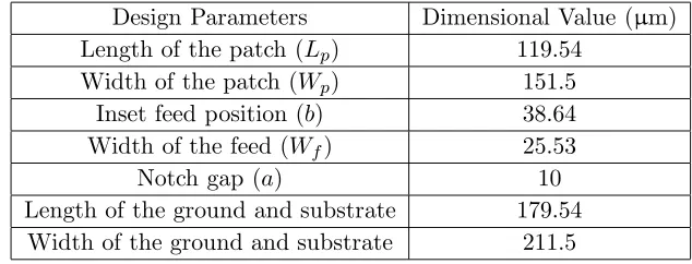
The studied microstrip antenna consists of a square radiating patch arranged on a dielectric substrate of permittivityεr= 3. A perfect electric conductor (PEC) ground plane is placed below the substrate and
participates in the radiation of the patch through the propagation of the field. The patch is supposed made of copper and fed by a copper excitation line as well. To determine the width Wp of the patch
antenna (Figure 1), we use the following equation:
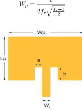
Wp = c 2fr
εr+1 2
(1)
where fr is the desired resonance frequency and c the light velocity. The bandwidth of the antenna depends on the width of the patchWp, and thus on the value ofεr. To include the effect of fringing fields
acting outside of the radiating patch in our calculations, we calculate the effective dielectric constant εreff given by:
εreff = εr
+ 1 2 +
εr−1
2
1 +12∗h Wp
(2)
The length of the patch,Lp, is calculated from Equation (3):
Lp=Leff −(2∗ΔL) (3)
where the effective length Leff is given by :
Leff = c
2fr√εreff
(4)
where ΔL is the fields overflow.
The length of the ground plane is calculated taking into account of the patch lengthLp according to:
Lg =Lp+ (6∗h) (5)
whereh is the substrate thickness.
The width of the ground plan and width of the feed line,Wg and Wf, respectively, are calculated from the following equations in order to obtain a characteristic impedance of the order of 50 Ω:
Wg=Wp+ (6∗h)
Wf =h
377 50√εr −2
(6)
The obtained values are tabulated in Table 1. In our calculations, the resonant frequency of the antenna is set to 0.7 THz. The thickness of the copper patch, as well as that of the microstrip, is 5µm. The thickness of the substrate used is 10µm.
Table 1. Dimensions of the studied microstrip patch antenna.
Design Parameters Dimensional Value (µm) Length of the patch (Lp) 119.54
Width of the patch (Wp) 151.5 Inset feed position (b) 38.64 Width of the feed (Wf) 25.53
Notch gap (a) 10
Length of the ground and substrate 179.54 Width of the ground and substrate 211.5
3. RESULTS AND DISCUSSION
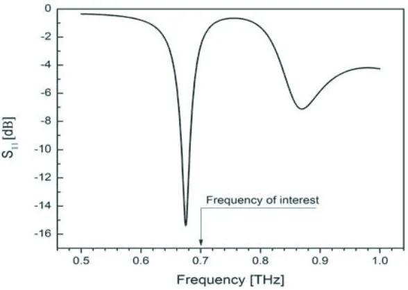
In Figure 2, we present the return loss characteristic of the microstrip patch antenna with the copper patch.
As depicted in this figure, the use of copper as patch material as well as feed line material gives a frequency of resonance at 0.68 THz with a return loss of only −15 dB. The gain of the antenna shown in Figures 3(a) and 3(b) is around 5.73 dB and is not a good gain, and we notice the presence of side lobes of about−13.8 dB.
Figure 2. Return loss of the copper-microstrip patch antenna.
(a) (b)
Figure 3. (a) 3D plot and (b) polar plot of far field Gain of copper-microstrip patch antenna at frequencyf = 0.7 THz (Main lobe magnitude = 5.63 dB, Main lobe direction = 0.0◦, Angular width at 3 dB = 82.1◦ and side lobe level =−13.9 dB).
To solve the problem of miniaturization, we can replace the copper patch by intelligent materials that have agile electromagnetic properties, so we use a graphene patch instead of the copper. With its 0.345 nm thickness, the graphene is a 2D material. We have replaced the volumetric patch made of copper which presents a thickness equal to 5 microns, by a planar patch with monoatomic thickness. In such a patch, the current density J is directly proportional to the surface conductivity σ as well as to the electric field via the formula:
J =σ E (7)
The graphene surface conductivity is a function of the frequency of the exciting electromagnetic wave, the temperature T, the chemical potential EF and the diffusion rate Γ of the carriers. This
of intra-band and inter-band transitions:
σ = σintra+σinter (8)
σintra = −j e
2k
BT
π2(ω−jΓ)
EF
kBT + 2 ln
1 +e
−EF
kBT
(9)
σinter = −je
2
4πln
2|EF| −(ω−jΓ) 2|EF|+ (ω−jΓ)
(10)
wherekBis the Boltzmann constant,the reduced Planck constant, T the temperature,ωthe pulsation
of the electromagnetic wave, EF the Fermi level, and Γ the diffusion rate (independent of energy).
The termσinter, based on a Fermi-Dirac distribution, allows taking the effects of temperature, doping
(displacement of the Fermi level with respect to the Dirac point) in addition to limits the transitions according to the position of the Fermi level (Principle of exclusion of Pauli). This blocking of the transitions is raised for energies of the excitation wave greater than both 2|EF|and kBT.
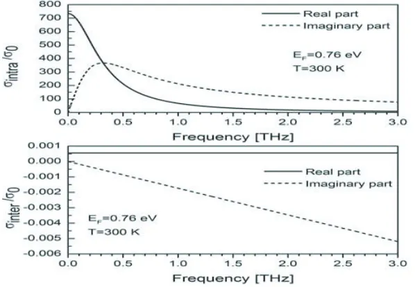
However,σintra depends essentially on the diffusion phenomena of the carriers in the graphene layer
and loses in contribution when the frequency of the excitation wave increases. Thus, the contributions of these two terms,σintra and σinter, depend on the range of frequencies considered. For the frequencies
smaller than 3 THz, which is our case, the contribution of the inter-band transitions to the conductivity becomes negligible (Figure 4). Now focusing on the intraband transitions contribution, in Figure 5 we present the variations of the complex intraband conductivity of graphene as a function of the Fermi EF level at the working frequency 0.7 THz. The variations of the real and the imaginary parts of the conductivity are linear and increase with EF.
Figure 4. Real part and imaginary part of the normalized complex surface conductivity of graphene in the range 0–3 THz. The contribution of the inter-transitions to the conductivity can be neglected compared to the intra-transitions one.
Figure 6 shows the return loss S11 for different values of the chemical potential EF which
corresponds to different values of the external applied electric field. From this figure, we can see a reconfiguration in the frequency of the coefficientS11. The resonant frequency can be tuned continuously
from 0.65 THz to 0.8 THz as Fermi level is shifted by the applied voltage gate.
The required resonating frequency of 0.7 THz is obtained for a Fermi level value of 0.76 eV as shown in Figure 7. For this value of EF, the return loss peak reaches −29 dB which is almost twice the value obtained with the copper patch.
Figure 5. Variation of the real and imaginary parts of the complex conductivity of graphene (intraband contribution) versus Fermi level valueEF. The variation is linear and increases withEF.
Figure 6. Graphene-microstrip patch antenna return loss adjustment vs Fermi level valueEF.
Figure 7. Comparison between the return loss of the copper-microstrip patch antenna and the return loss of the graphene-microstrip patch antenna. For the graphene patch, the return loss peak reaches
(a) (b)
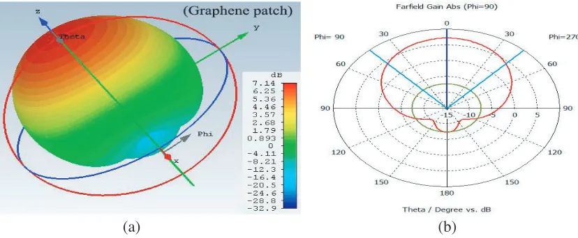
Figure 8. (a) 3D plot and (b) polar plot of far field gain of graphene-microstrip patch antenna at frequencyf = 0.7 THz (Main lobe magnitude = 7.11 dB, Main lobe direction = 0.0◦, Angular width at 3 dB = 85.8◦ and side lobe level =−16.8 dB).
mobility of the electrons in the graphene. This amplification is also reflected by the attenuation of the secondary lobes which reach −16.8 dB.
4. CONCLUSION
The comparison of the radiation properties of a patch antenna where the patch is made either of Copper or Graphene show that the surface conductivity of graphene allows a reconfiguration of the radiating proprieties. We show that the adjustment of the Fermi level of graphene, with the application of an external electrical field, to the value of 0.76 eV allows obtaining a return loss value twice that of copper at 0.7 THz which is the frequency of interest in aerospace applications. This increase in the return loss peak is also accompanied by an improvement in the gain of the antenna.
REFERENCES
1. Jornet, J. M. and I. F. Akyildiz, “Graphene-based nano-antennas for electromagnetic nanocommunications in the terahertz band,” Antennas Propag. EuCAP 2010 Proc. Fourth Eur. Conf., 1–5, 2010.
2. Geiˇzutis, A., A. Krotkus, K. Bertulis, G. Molis, R. Adomaviˇcius, A. Urbanowicz, et al., “Terahertz radiation emitters and detectors,”Opt. Mater. (Amst)., Vol. 30, 786–788, 2008.
3. Siegel, P. H., “Terahertz technology,” IEEE Trans. Microw. Theory Tech., Vol. 50, 910–928, 2002. 4. Zhu, B., Y. Chen, K. Deng, W. Hu, and Z. S. Yao, “Terahertz science and technology and
applications,” PIERS Proceedings, 1166–1170, Beijing, China, Mar. 23—27, 2009.
5. Koutsoupidou, M., I. S. Karanasiou, and N. Uzunoglu, “Rectangular patch antenna on split-ring resonators substrate for THz brain imaging: Modeling and testing,” 13th IEEE Int. Conf. Bioinforma. Bioeng. IEEE BIBE 2013, 9–12, 2013.
6. Kashyap, S. S. and V. Dwivedi, “Stacked swastika shape microstrip patch antenna for terahertz applications,”Proc. 2014 2nd Int. Conf. “Emerging Technol. Trends Electron. Commun. Networking”, ET2ECN 2014, 1–5, 2015.
7. Tan, P., J. Huang, K. Liu, Y. Xiong, and M. Fan, “Terahertz radiation sources based on free electron lasers and their applications,”Sci. China Inf. Sci., Vol. 55, 1–15, 2012.
9. Pierantoni, L., M. Bozzi, R. Moro, D. Mencarelli, and S. Bellucci, “On the use of electrostatically doped graphene: Analysis of microwave attenuators,”2014 Int. Conf. Numer. Electromagn. Model. Optim. RF, Microwave, Terahertz Appl. NEMO 2014, 8–11, 2014.
10. Kemp, M. C., P. F. Taday, B. E. Cole, J. A. Cluff, A. J. Fitzgerald, and W. R. Tribe, Security Applications of Terahertz Technology, Vol. 5070, 44–52, 2003.
11. Watts, C. M., D. Shrekenhamer, J. Montoya, G. Lipworth, J. Hunt, T. Sleasman, et al., “Terahertz compressive imaging with metamaterial spatial light modulators,”Nat. Photonics, Vol. 8, 605–609, 2014.
12. Siegel, P. H., “THz Technology in biology and medicine, instrumentation,”IEEE Transactions on Microwave Theory and Techniques, Vol. 52, 0–3, 2004.
13. Cai, Y., Y. J. Guo, P. Y. Qin, and A. R. Weily, “Frequency reconfigurable quasi-Yagi dipole antenna,” 2010 IEEE Int. Symp. Antennas Propag. CNC-USNC/URSI Radio Sci. Meet. — Lead. Wave, AP-S/URSI 2010, Vol. 58, 2742–2747, 2010.
14. Piazza, D., P. Mookiah, M. D’Amico, and K. R. Dandekar, “Pattern and polarization reconfigurable circular patch for MIMO systems,” 3rd European Conference on Antennas Propagation, 2009, EuCAP 2009, Vol. 59, 1047–1051, 2009.
15. Chang, Z., L. S. Wu, M. Tang, Y. P. Zhang, and J. F. Mao, “Generation of THz wave with orbital angular momentum by graphene patch reflectarray,” 2015 IEEE MTT-S Int. Microw. Work. Ser. Adv. Mater. Process. RF THz Appl. IEEE MTT-S IMWS-AMP 2015 — Proc., 9–11, 2015. 16. Mazlouman, S. J., M. Soleimani, A. Mahanfar, C. Menon, and R. G. Vaughan, “Pattern
reconfigurable square ring patch antenna actuated by hemispherical dielectric elastomer,”Electron. Lett., Vol. 47, 164–U22, 2011.
17. Surface, H., Y. Huang, L.-S. Wu, M. Tang, J. Mao, and H. Surface, “Design of a beam reconfigurable THz antenna with graphene-based switchable,” IEEE Trans. Nanotechnology, Vol. 11, 836–842, 2012.
18. Geim, A. K. and K. S. Novoselov, “The rise of graphene,”Nat. Mater., Vol. 6, 183–191, 2007. 19. Falkovsky, L. A., “Optical properties of graphene,”Journal of Physics: Conference Series, Vol. 129,
1, 2008.
20. Loh, K. P., Q. Bao, G. Eda, and M. Chhowalla, “Graphene oxide as a chemically tunable platform for optical applications,”Nat. Chem., Vol. 2, 1015–1024, 2010.
21. Castro Neto, A. H., N. M. R. Peres, K. S. Novoselov, and A. K. Geim, “The electronic properties of graphene,”Rev. Mod. Phys., Vol. 81, 109–162, 2009.
22. Ajlani, H., M. K. Azizi, A. Gharsallah, and M. Oueslati, “Graphene-GaAs-graphene stacked layers for the improvement of the transmission at the wavelength of 1.55µm,” Opt. Mater., Vol. 57, 120–124, 2016.
23. Ajlani, H., M. Karim, A. Gharsallah, and A. Meftah, “Graphene-based reconfigurable transmission filter near the wavelength of 1. 55µm,” Opt. Mater., Vol. 66, 201–206, 2017.
24. Zhang, J., G. Wang, B. Zhang, T. He, Y. He, and J. Shen, “Photo-excited broadband tunable terahertz metamaterial absorber,”Opt. Mater. (Amst)., Vol. 54, 32–36, 2016.
25. Hanson, G. W., “Dyadic Green’s functions and guided surface waves for a surface conductivity model of graphene,”J. Appl. Phys., 103, 2008.