A modified z-source boost dc-dc converter for photovoltaic applications
J. Rajitha , T. Vigneysh , Dr.P.Sridhar
M-tech Student Scholar
Department of Power Electronics and Electrical Drives, Institute of Aeronautical Engineering, Dundigal, Hyderabad, Telangana, India. Email: [email protected]
Assistant Professor Department of Power Electronics and Electrical Drives, Institute of Aeronautical Engineering, Dundigal, Hyderabad, Telangana, India.
Email: [email protected]
Department of Power Electronics & Electrical Drives, ( H.O.D ) Institute of Aeronautical Engineering (IARE) , Dundigal, Hyderabad; Telangana, India
Email:[email protected]
Abstract; Now a day’s the rate of energy generated by the renewable energy sources are increasing rapidly. More popular source form these sources is the photovoltaic system source, but this photovoltaic system is now also most costly and a research work is going on to reduce the cost and increase efficiency of photovoltaic system. boost dc-dc converter system is developed for to convert dc power in to the dc and also boost dc output. Due to less no of switches, complicity of converter has been reduced. However the conventional boost converter capabilities are limited.Hence ,in this work, we have proposed a new topology based a Z-source configuration to interface the pv system .The boosting capability of conventional boost dc –dc Z-source converter is limited.Hence to overcome the limitations of conventional Z-source boost dc-dc converter, a modified version of Z-source boost dc-dc converter is proposed with stronger voltage boost capabilities. The performance of the proposed converter for photovoltaic application is successfully verified using Matlab Simulation.
I. INTRODUCTION
Nowadays the use of power is increased because of the increased population and use of more number of electronic equipments among which some will be high power rated devices. So there is a demand for large amount of power generation in these days and even it will keep increasing in the future generation. So technologies are developed to generate the large amount of power using the available sources of energy in the nature, which is cost efficient and environmental friendly. The renewable energy sources are available in the form of sun, wind, tidal, biomass and others. Using sun as the source of energy photovoltaic systems are developed. But the output obtained from the photovoltaic panels is of low value, so there is a need of step up of the output voltage from the PV panels. Because the low value voltage cannot be provided to the inverters. Hence the design oh step up dc-dc converters is most. important in PV systems. Till now, many voltage-boost topologies have been explored, namely voltage multiplier, switched-inductor, switched.
and C circuits are formed namely quasi z source networks.
Quasi z source network has both current fed topology and voltage fed topology which is similar to the z source network. Disadvantages with the z source converter are discontinuity of input.current, greater.voltage stress on Switch is more. The Lf-Cf output filter is used to reduce ripple in the output.current and load voltage respectively [2]. In the reference [21] & [22] authors have used the MPPT algorithm to obtain the maximum power while harnessing the solar energy.
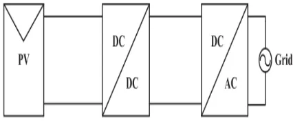
IN THE last several years, with the tension of global fossil en- ergy, the renewable energy power systems, which are mainly on the photovoltaic (PV) power systems, are developing rapidly. In a PV power system, the output voltages of the PV panels are usually low and vary widely under the influences of weather and environment, therefore a step-up stage is often demanded [1]–[3]. The two-stage systems are shown in Fig. 1, which consist of step-up dc–dc converters and inverters. The unregulated low dc voltage of PV panels, which cannot be provided for inverters, must be boosted and regulated through the high-gain converters. Then, the step-up converters output regulated high dc voltage to the grid-connected inverters.
Thus, the design of the step-up dc–dc converters is very important to the PV power systems. So far, various voltage-boost techniques have been greatly explored, such as the voltage multiplier [4], switched inductor [5], switched capacitor [6], coupled inductor [7], voltage lift [8], and cascaded boost [9] techniques. However, these techniques are all complex with low efficiency and high costs.
Fig..1. Two-stage PV power systems.
Fig. 2. Z-source inverter
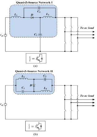
The concept of Z-source network was first proposed by Peng [10]. As shown in Fig. 2, the Z-source network is an X-shaped impedance network, which can be applied to dc–ac, dc–dc, ac–ac, and ac–dc power conversion. The Z-source inverter (ZSI) can utilize the shoot-through state which is not allowed in the traditional voltage-source inverters to boost the voltage. In addition, the buck voltage inversion ability is also retained. The ZSI has rapidly become a research hotspot because of its buck– boost inversion ability. Though with the aforementioned advantages, the original ZSI also has some drawbacks, such as discontinuous input current, high-voltage stresses, and limited boost factor 1/(1−2DS ) (DS is the shoot-through duty cycle). Moreover, the dc voltage source and the inverter bridge do not share a common ground. To overcome the limitations in the original ZSI, various novel impedance-source network topologies have been presented in numerous studies [11]–[24]. Among the modified Z-source network topologies, quasi-Z-source network is a simple but efficient solution [11]–[13]. It can be seen from Fig. 3 that the quasi Z-source inverters (qZSI) can be classified into continuous current qZSI and discontinuous-current qZSI. For easier referencing, their impedance networks are, respectively, referred to as quasi-Z-source network I and quasi-Z-source network II. The two proposed quasi-Z-source networks have the same boost factors as the traditional Z-source network, which are 1/(1−2DS ), but they have some advantages over the traditional Z-source network, such as continuous input current, common ground between the voltage source and the inverter bridge, and reduced capacitor voltage stress.
applies the Z-source networks to dc–dc converters with their boost abilities, and proposes a family of hybrid Z-source boost dc–dc converter, which is obtained by combining the traditional Z-source/quasi-Z-source networks in different ways. As a result, the integrations of the Z-source/quasi-Z-source networks enhance the boost abilities of the obtained hybrid Z-source networks and retain all the advantages of the traditional Z-source/quasi-Z-source networks. Due to the aforementioned advantages, the proposed converters are very suited for PV power systems, where the dc–dc converter with high step-up ability is often demanded. Like the traditional Z-source network, the proposed hybrid Z-Z-source networks also can be applied to dc–ac, ac–ac, and ac–dc power conversions.
Fig. .3. Quasi-Z-source inverters. (a) Continuous-current qZSI. (b) Discontinuous-current qZSI.
of Z-source networks in dc–dc power conversion is still a gap to fill. Therefore, this paper applies the Z-source networks to dc–dc converters with their boost abilities, and proposes a family of hybrid Z-source boost dc–dc converter, which is obtained by combining the traditional Z-source/quasi-Z-source networks in different ways. As a result, the integrations of the Z-source/quasi-Z-source networks enhance the boost abilities of the obtained hybrid Z-source networks and retain all the advantages of the traditional Z-source/quasi-Z-source networks. Due to the aforementioned advantages, the proposed converters are very suited for PV power systems, where the dc–dc converter with high step-up ability is often demanded. Like the traditional Z-source network, the proposed
hybrid Z-source networks also can be applied to dc–ac, ac–ac, and ac–dc power conversions.
4.2 CONFIGURATION OF THE PROPOSED CONVERTER
Three new hybrid Z-source dc–dc converters are presented in this paper, which can be categorized as hybrid two-quasi-Z source boost dc–dc converter, hybrid three-quasi-Z-source boost dc–dc converter, and hybrid Z-source/quasi-Z-source boost dc– dc converter. The topologies of these converters are presented in the following sections.
4.2.1 Hybrid Two-Quasi-Z-Source Boost DC–
DC Converter
Fig. 4. Hybrid two-quasi-Z-source boost dc–dc converter. The hybrid two-quasi-Z-source boost dc–dc converter is shown in Fig. 4, which consists of a hybrid two-quasi-Zsource network (L1−D1−C1−C2−L2−C3−D2−C4−L3), an active switch S, an output diode D3, and an output capacitor C5. It can be seen from Fig. 4 that the proposed hybrid Z-source network is obtained by replacing an inductor L2 in the quasi-Z-source network1 I with the quasi-Z-source network II, which adds an inductor L3, two capacitors (C3 and C4), and a diode D2 to the quasi-Z-source network I. The hybrid two-quasi-quasi-Z-source network has higher step-up ability (voltage gain M = 1/(1 − 3Ds)) than that of the quasi-Z-source network I (M = 1/(1 − 2Ds)) and inherits the merits of the quasi-Z-source network I, such as continuous input current and common ground between the input and output.
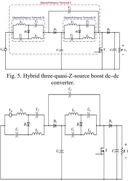
Similar to the aforementioned topology, the proposed hybrid Z-source network in this section is the integration of the quasi-Z-source network I and quasi-Z-source network II. Fig. 5 shows the hybrid three-quasi-Z-source boost dc–dc converters. It can be noticed that the proposed hybrid Z source network (L1−C1−D1−C2−L2−D2−C3−C4−L3−C5−D3−C6− L4) is obtained by replacing all the inductors (L1 and L2) in the quasi-Z-source network I with the quasi-Z-source network II. In addition to the hybrid three-quasi-Z-source network, the proposed converter employs an active switch S, an output diode D4, and an output capacitor C7. Though the voltage gain (M = 1/(1 − 4Ds)) of the proposed converter is higher than that of the hybrid two-quasi-Z-source boost dc–dc converter, it draws a discontinuous current from the dc voltage source.
Fig. 5. Hybrid three-quasi-Z-source boost dc–dc converter.
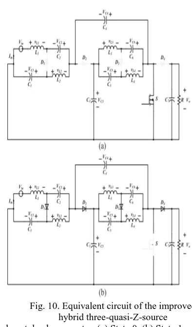
Fig. 6. Improved hybrid three-quasi-Z-source boost dc–dc converter.
To smooth the input current, a simple improvement on the proposed converter is shown in Fig. 6, where dc voltage source is placed in series with the inductor L1. However, the voltage gain of the improved hybrid three-quasi- Z-source boost dc–dc converter is not influenced by the modification, which is the same as the hybrid three-quasi-Z-source boost dc–dc converter. In addition to the
high-voltage gain and continuous input current, the improved hybrid three-quasi Z-source network provides a common ground between the input and output.
4.2.3 Hybrid Z-Source/Quasi-Z-Source Boost DC–DC Converter
Fig. 7. Hybrid Z-source/quasi-Z-source boost dc–dc converter.
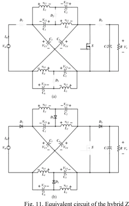
This section proposes a hybrid Z-source network which combines the original Z-source network with the quasi-source network II. As shown in Fig. 7, the proposed
Z-source network(L1
−C1−D2−C2−L2−C3−C4−L3−C5−D3−L4− C6) replaces the inductors (L1 and L2) in the original Z-source network with the quasi-Z-source network II. Additionally, the proposed converter comprises an active switch S, two diodes (D1 and D4), and an output capacitor C7. Like the traditional Z-source network, the hybrid Z-source/quasi-Z-source network has a symmetrical structure, and the step-up ability (M = 1/(1 − 4Ds)) of the propose hybrid Z-source network is similar to that of the hybrid three-quasi-Z-source network.
4.3 OPERATING PRINCIPLES OF THE
PROPOSED CONVERTERS
The operating principles of the proposed converters are analyzed in this section. For analytical purposes, the following conditions are assumed.
1) All the components are ideal.
2) 2) All capacitors are so large that the capacitor voltages can be treated as constant.
3) All the proposed converters operate in CCM.
4.3.1 Hybrid Two-Quasi-Z-Source Boost DC–
Fig..8. Key waveforms of the hybrid Z-source networks.
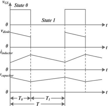
The operation principles of the proposed converters are similar to that of the novel Z-source dc–dc converter [25]. Fig. 4.8 shows the key waveforms of the hybrid Z-source networks. The operation states of all the proposed converters can be divided into two states: state 0 and state 1.
4.3.1.1 State 0: The equivalent circuit of the proposed converter operates in state 0 is shown in Fig. 9(a). During this state, the switch S is ON, while diodes D1−D3 are OFF. Assuming that T0 = DT is the interval of state 0 in a switch cycle T, where D is the duty cycle. The voltage source Vin and capacitor C2 discharge the energy to inductor L1. Inductors L2 and L3 are charged by
capacitors C1, C3, and C4. quasi-Z-source boost dc–dc converter. (a) State Fig. 9. Equivalent circuit of the hybrid
two-0. (b) State 1.
According to Kirchhoff’s Voltage Law (KVL), the voltages across inductors L1 − L3 can be expressed as
(1) Due to the symmetry of the quasi-Z-source network II (L2 = L3, C3 = C4), we obtain
(3) By applying the voltage–second balance principle to the inductors L1 and L2 (or L3) from (1)–(3), we have
(4) Thus, the voltage gain M of the proposed converter can be expressed as
(5) From (5), we know that the step-up ability of the proposed hybrid Z-source network is higher than that of the traditional Z-source/quasi-Z-source network and the switched-inductor quasi-Z-source network [17].
4.3.2 Improved Hybrid Three-Quasi-Z-Source Boost DC–DC Converter
Because the hybrid three-quasi-Z-source boost dc–dc converter and the improved hybrid three-quasi-Z-source boost dc– dc converter have the same voltage gain, we take the latter as an example to analyze. The improved hybrid three-quasi-Z-source boost dc–dc converter also has two operation states: state 0 and state 1.
4.3.2.1 State 0: Fig. 10(a) shows the equivalent circuit of the proposed converter operates in state 0. During this state, switch S is ON, while diodes D1−D4 are OFF. Capacitors C1−C6 discharge the energy to inductors L1−L4. By applying KVL to Fig. 10(a), the following equations can be derived:
Fig. 10. Equivalent circuit of the improved hybrid three-quasi-Z-source boost dc–dc converter. (a) State 0. (b) State 1.
4.3.2.2 State 1: Fig. 10(b) shows the equivalent circuit of the proposed converter operates in state 1. During this state, switch S is OFF, while diodes D1−D4 are ON. Inductors L1–L4 transfer energy to capacitors C1−C6 and the load R. The following equations can be obtained according to the equivalent circuit in state 1:
(8) By applying the voltage–second balance principle to the inductors L1−L3 (or L4), we have
(9) The voltage gain M of the proposed converter is
It can be seen from (10) that the boost ability of the proposed hybrid Z-source network is stronger than that of the hybrid two-quasi-Z-source network. Moreover, they have the same advantages.
4.3.3 Hybrid Z-Source/Quasi-Z-Source Boost DC–DC Converter
The hybrid Z-source/quasi-Z-source boost dc–dc converter has two operating states: state 0 and state 1.
4.3.3.1 State 0: Fig. 11(a) shows the equivalent circuit diagram for state 0. During this state, the switch S is ON, while diodes D1−D4 are OFF. All the capacitors discharge the energy to all the inductors. The following equations can be derived because of the symmetries of the Z-source network (C3 = C4) and quasi-Z-source network II (L1 = L2 = L3 = L4, C1 = C2 = C5 = C6)
Fig. 11. Equivalent circuit of the hybrid Z-source/quasi-Z-source boost dc–dc converter. (a) State 0. (b) State 1.
(11) As shown in Fig. 11(a), we have
(12)
4.3.3.2 State 1: Fig. 11(b) shows the equivalent circuit diagram for state 1. During this state, the switch S is OFF, while diodes D1−D4 are ON. The voltage source Vin and inductors transfer the energy to the capacitors and the load R. The following relationships can be obtained:
(13) By applying the voltage–second balance principle to the inductors L1, we have
(14) Thus, the voltage gain M of the proposed converter is
(15) Even though the hybrid Z-source/quasi-Z-source network has the same boost ability as the improved hybrid three-quasi-Zsource network, it does not provide the continuous input current and common ground between the input and output.
4.3.4 Impact of Component Losses on Output Voltage
In fact, the losses of each component could affect the step-up performances of the proposed converters. We assume that the dc resistances of the inductors are rL, the forward voltage drops of the diodes are VD , the on resistance of the switch is rs, and the average input current is Iin. For the hybrid two-quasi-Z-source boost dc–dc converter, the output voltage Vo can be expressed as
(16) For the improved hybrid three-quasi-Z-source boost dc– dc converter, the output voltage Vo is
(18)
6. PHOTOVOLTAIC TECHNOLOGY
A PV array consists of a number of PV modules, mounted in the same plane and electrically connected to give the required electrical output for the application. The PV array can be of any size from a few hundred watts to hundreds of kilowatts, although the larger systems are often divided into several electrically independent sub arrays each feeding into their own power conditioning system.
Photovoltaic’s is the field of technology and research related to the devices which directly convert sunlight into electricity using semiconductors that exhibit the photovoltaic effect. Photovoltaic effect involves the creation of voltage in a material upon exposure to electromagnetic radiation.
The photovoltaic effect was first noted by a French physicist, Edmund Becquerel, in 1839, who found that certain materials would produce small amounts of electric current when exposed to light. In 1905, Albert Einstein described the nature of light and the photoelectric effect on which photovoltaic technology is based, for which he later won a Nobel prize in physics. The first photovoltaic module was built by Bell Laboratories in 1954. It was billed as a solar battery and was mostly just a curiosity as it was too expensive to gain widespread use. In the 1960s, the space industry began to make the first serious use of the technology to provide power aboard spacecraft. Through the space programs, the technology advanced, its reliability was established, and the cost began to decline. During the energy crisis in the 1970s, photovoltaic technology gained recognition as a source of power for non-space applications.
The solar cell is the elementary building block of the photovoltaic technology. Solar cells are made of semiconductor materials, such as silicon. One of the properties of semiconductors that makes them most useful is that their conductivity may easily be modified by introducing impurities into their crystal lattice. For instance, in the fabrication of a photovoltaic solar cell, silicon, which has four valence electrons, is treated to increase its conductivity. On one side of the cell, the impurities, which are phosphorus atoms with five valence electrons (n-donor), donate weakly bound valence electrons to the silicon material, creating excess negative charge carriers.
On the other side, atoms of boron with three valence electrons (p-donor) create a greater affinity than silicon to attract electrons. Because the p-type silicon is in intimate contact with the n-type silicon a p-n junction is established and a diffusion of electrons occurs from the region of high electron concentration (the n-type side) into the region of low electron concentration (p-type side). When the electrons diffuse across the p-n junction, they recombine with holes on the p-type side.
However, the diffusion of carriers does not occur indefinitely, because the imbalance of charge immediately on either sides of the junction originates an electric field. This electric field forms a diode that promotes current to flow in only one direction.
Ohmic metal-semiconductor contacts are made to both the n-type and p-type sides of the solar cell, and the electrodes are ready to be connected to an external load. When photons of light fall on the cell, they transfer their energy to the charge carriers. The electric field across the junction separates photo-generated positive charge carriers (holes) from their negative counterpart (electrons). In this way an electrical current is extracted once the circuit is closed on an external load.
Fig: 12. photovoltaic system
(B) PV CELL MODEL
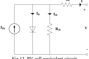
The equivalent circuit of a PV cell is shown in Fig.4.3. It includes a current source, a diode, a series resistance and a shunt resistance.
IPh Rsh
ID Ish
Rs I
+
V
I = 𝐼𝑝ℎ - 𝐼𝑠(exp 𝑞(𝑉+ 𝑅𝑠I)
𝑁𝐾𝑇 ) -1) – (𝑉+ 𝑅𝑠I)
𝑅𝑠ℎ
(4.1)
In this equation, Iphis the photocurrent, Isis the reverse saturation current of the diode, q is the electron charge, V is the voltage across the diode, K is the Boltzmann's constant, T is the junction temperature, N is the ideality factor of the diode, and Rsand Rshare the series and shunt resistors of the cell, respectively. As a result, the complete physical behavior of the PV cell is in relation with Iph, Is, Rsand Rshfrom one hand and with two environmental parameters as the temperature and the solar radiation from the other hand.
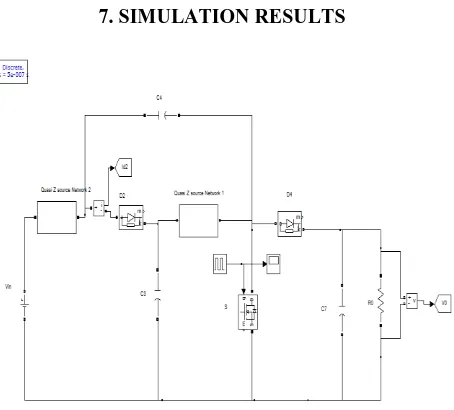
7. SIMULATION RESULTS
Fig.14: Hybrid three-quasi-z-source
Fig.15:ID1,ID2,ID3,IL1( Charging and Discharging current)
Fig.16:VC1,VC2,V0 (Charging and Discharging voltage)
Fig.17:VGS(gate pulses)
Fig. 18: Hybrid two-quasi-z-source
Fig.20:.VC1,VC2,V0(Charging and Discharging voltage)
Fig.21:V0 (output voltage)
Fig.22:VGS (gate pulses)
Fig.23:.PV_Hybridthree_quasi-z-source
Fig.24:ID1,ID2,ID3,IL1(Charging and Discharging current)
Fig.25 : VC1,VC2,V0(Charging and Discharging voltage)
Fig.26.: VGS (gate pulses)
Fig.27:.V0 (output voltage)
8. CONCLUSION
A family of hybrid Z-source boost dc–dc converters for PV power systems has been presented in this paper. The proposed converters use the hybrid Z-source networks, which are obtained by combining the traditional Z-source networks. Apart from the high step-up abilities, the proposed hybrid Z-source networks retain all the advantages of the traditional Z-source networks, such as continuous input current, reduced capacitor voltage stress, and common ground between the voltage source and the inverter bridge. The topologies, operating principles, and comparison with other Z-source networks are presented in this paper. Finally, the simulation and experimental results verify the features of the proposed converters.
REFERENCES
[2] Y. P. Hsieh, J. F. Chen, T. J. Liang, and L. S. Yang, “Novel high stepup dc-dc converter for distributed generation systems,” IEEE Trans. Ind. Electron., vol. 60, no. 4, pp. 1473–1482, Apr. 2013.
[3] B. Ge et al., “An energy stored quasi-Z-source inverter for application to photovoltaic power systems,” IEEE Trans. Ind. Electron., vol. 60, no. 10, pp. 4468–4481, Oct. 2013.
[4] M. Prudente, L. L. Pfitscher, G. Emmendoerfer, E. F. Romaneli, and R. Gules, “Voltage multiplier cells applied to non-isolated dc-dc converters,” IEEE Trans. Power Electron., vol. 23, no. 2, pp. 871–887, Mar. 2008.
[5] B. Axelrod, Y. Berkovich, and A. Ioinovici, “Switchedcapacitor/switched-inductor structures for getting transformerless hybrid dc-dc PWM converters,” IEEE Trans. Circuits Syst. I, Reg. Papers, vol. 55, no. 2, pp. 687–696, Mar. 2008.
[6] O. Abutbul, A. Gherlitz, Y. Berkovich, and A. Ioinovici, “Step-up switching-mode converter with high voltage gain using a switchedcapacitor circuit,” IEEE Trans. Circuits Syst. I, Fundam. Theory Appl., vol. 50, no. 9, pp. 1098–1102, Aug. 2003.
[7] R. J. Wai, C. Y. Lin, R. Y. Duan, and Y. R. Chang, “High-efficiency dc-dc converter with high voltage gain and reduced switch stress,” IEEE Trans. Ind. Electron., vol. 54, no. 1, pp. 354–364, Jan. 2007.
[8] F. L. Luo, “Six self-lift dc-dc converters,” IEEE Trans. Ind. Electron., vol. 48, no. 6, pp. 1268–1272, Dec. 2001.
[9] L. Huber and M. M. Milanovic, “A design approach for server power supplies for networking applications,” in Proc. IEEE Appl. Power Electron. Conf. Expo., 2000, pp. 1163–1169.
[10] F. Z. Peng, “Z-source inverter,” IEEE Trans. Ind. Appl., vol. 39, no. 2, pp. 504–510, Mar./Apr. 2003. [11] J. Anderson and F. Z. Peng, “Four quasi-Z-source inverters,” in Proc. IEEE Power Electron. Spec. Conf., Jun. 2008, pp. 2743–2749.
[12] Y. Tang, S. Xie, C. Zhang, and Z. Xu, “Improved Z-source inverter with reduced Z-Z-source capacitor voltage stress and soft-start capability,” IEEE Trans. Power Electron., vol. 24, no. 2, pp. 409–415, Feb. 2009.
[13] M. K. Nguyen, Y. G. Jung, and Y. C. Lim, “Single-phase ac-ac converter based on quasi-Z-source topology,” IEEE Trans. Power Electron., vol. 25, no. 8, pp. 2200– 2210, Aug. 2010.
[14] Y. Tang, S. Xie, and C. Zhang, “An improved Z-source inverter,” IEEE Trans. Power Electron., vol. 26, no. 12, pp. 3865–3868, Dec. 2011.
[15] M. Zhu, K. Yu, and F. L. Luo, “Switched-inductor Z-source inverter,” IEEE Trans. Power Electron., vol. 25, no. 8, pp. 2150–2158, Aug. 2010.
[16] C. J. Gajanayake, F. L. Luo, H. B. Gooi, and L. K. Siow, “Extendedboost Z-source inverters,” IEEE Trans. Power Electron., vol. 25, no. 10, pp. 2642–2652, Oct. 2010.
[17] M. K. Nguyen, Y. C. Lim, and G. B. Cho, “Switched-inductor quasiZ-source inverter,” IEEE Trans. Power Electron., vol. 26, no. 11, pp. 3183–3191, Nov. 2011.
[18] M. K. Nguyen, Y. C. Lim, and Y. G. Kim, “TZ-source inverters,” IEEE Trans. Ind. Electron., vol. 60, no. 12, pp. 5685–5695, Dec. 2013.
[19] D. Li, P. C. Loh, M. Zhu, F. Gao, and F. Blaabjerg, “Enhanced-boost Z-source inverters with alternate-cascaded switched- and tapped-inductor cells,” IEEE Trans. Ind. Electron., vol. 60, no. 9, pp. 3567–3578, Sep.2013.
[20] W. Mo, P. C. Loh, and F. Blaabjerg, “Asymmetrical Г-source inverters,” IEEE Trans. Ind. Electron., vol. 61, no. 2, pp. 637–647, Feb. 2014.
[21] L. Pan, “L-Z-source inverter,” IEEE Trans. Power Electron., vol. 29, no. 12, pp. 6534–6543, Dec. 2014.
[22] G. Zhang, B. Zhang, Z. Li, D. Qiu, L. Yang, and W. A. Halang, “A 3- Z-network boost converter,” IEEE Trans. Ind. Electron., vol. 62, no. 1, pp. 278–288, Jan. 2015.
[23] Y. P. Siwakoti, P. C. Loh, F. Blaabjerg, S. J converter for distributed generation,” IEEE Trans. Ind. Electron., vol. 62, no. 2, pp. 1059–1069, Feb. 2015. [24] H. F. Ahmed, H. Cha, S. H. Kim, and H. G. Kim, “Switched-coupledinductor quasi-Z source inverter,” IEEE Trans. Power Electron., vol. 31, no. 2, pp. 1241– 1254, Feb. 2016.
[25] X. Fang, “A novel Z-source dc-dc converter,” in Proc. IEEE Int. Conf. Ind. Technol., 2009, pp. 574–78
.
Author – 1 J.RAJITHA
M-tech Student Scholar
Department of Power Electronics and Electrical Drives, Institute of Aeronautical Engineering, Dundigal, Hyderabad, Telangana, India.
Author - 2 T. Vigneysh
Assistant Professor
Department of Electrical & Electronics Engineering, Institute of Aeronautical Engineering, Dundigal, Hyderabad, Telangana, India.
Email: [email protected]
Author – 3
P. SridharProfessor (H.O.D)
Department of Electrical & Electronics Engineering, Institute of Aeronautical Engineering, Dundigal, Hyderabad, Telangana, India.