A Compact Dispersive Delay Line Using Microstrip Lines
and Opened Slot Lines
Yujie Li, Jiade Yuan*, Shiji Wu, and Zhimeng Xu
Abstract—A dispersive delay line (DDL) with compact size, good group delay, and all pass response in 200–800 MHz band is presented. The proposed DDL is composed of a main microstrip transmission line with two shunted open stubs and two complementary slot lines, and a coupling slot line in ground plane. The length of the complementary slot line is reduced approximately from λg/2 toλg/4 through the upper end being opened, hence achieves miniaturization for the proposed DDL (λg is the guided wavelength at the center frequency). The overall area is 0.196×0.093λ2g with a peak group delay time of 3.2 ns. The proposed DDL has the advantages of compactness, good capability, and easy fabrication without any external matching network.
1. INTRODUCTION
A dispersive delay line (DDL) can provide frequency dependent group delay. It is widely used in many areas, such as group delay equalization, novel phase array elements, compressive receiver, and analog signal processing [1–9]. At present, a key research challenge for DDL is to achieve high delay from a compact structure with an acceptable insertion loss (IL). In [10], a DDL using microstrip line technology that contains shunt open-stub overlapping a shorted slot line is presented. The DDL has all-pass magnitude response over ultra-wideband frequency range and provides a smooth and continuous group delay profile. In [11], the DDL theories of microstrip line technology are further developed, and analytical expressions that contain the transmission coefficient (|S21|) and group delay (GD) are derived.
In [12], two deformed open stubs and their complementary slot lines are used to obtain a DDL with all-pass magnitude respond and good group delay. Although there are some distinguished advantages in [10–12] for the DDL using microstrip line technology, the miniaturization of the DDL is crucial to the practical application, especially for operating in the low frequency band. However, both the open stubs and their complementary short slot lines in [10–12] are about a half guide wavelength (λg/2) and located on both sides of the main transmission line symmetrically, which occupy a relative large space accordingly.
In this letter, we propose a novel compact DDL design that can locate the open stubs and their complementary slot lines on the same side of the main transmission line. The proposed complementary slot line has the length aboutλg/4, rather than aboutλg/2 in [10–12]. Moreover, an additional coupling slot line is embedded transversely in ground plane for fine-tuning the impedance matching.
2. DESIGN OF THE DDL
The configuration of the proposed DDL is shown in Fig. 1. The DDL is built on an IT-8350G substrate with relative permittivity of 3.5, loss tangent of 0.0025, and thickness of 0.5 mm, respectively. Two
Received 4 May 2019, Accepted 8 July 2019, Scheduled 21 July 2019
* Corresponding author: Jiade Yuan ([email protected]).
W
L W0
W1 W2
d1 Lg
L1
L2 L3
Port 1 Port 2
Open stub Main transmission line
C
om
ple
m
ent
ary sl
ot
line
s
Coupling slot line
d2
(a) (b)
Figure 1. Geometry of the proposed DDL, (a) top view, (b) bottom view.
0.2 0.4 0.6 0.8
Freq (GHz) 0
-10
-20
-30
-40
-50
|
S
| (dB)
11 short
open
open slot short slot
Figure 2. Simulated|S11|for the open slot and short slot of the upper end.
shunted open stubs with each length about λg/4 are located on the same side of the main transmission line, where open stubs are folded back for saving space, as shown in Fig. 1(a). Three slot lines with the same width of W2 are etched in ground plane, where two slot lines of them act as the complementary
slot lines, and the third slot line acts as the coupling line, as shown in Fig. 1(b).
|S11|
upper end of the complementary slot line is shorted, as shown in Fig. 2.
The performance of the proposed DDL is simulated, and the optimized design parameters are as follows (mm): L = 63, W = 30, L1 = 47.3, L2 = 7, L3 = 36, W0 = 1.9, W1 = 2, W2 = 0.7, Lg = 55,
d1 = 14, d2 = 3.5 mm.
3. PARAMETRIC STUDIES
Parametric studies are performed by simulating the DDL parameters of |S11|, |S21|, and group delay.
Only one geometrical parameter is varied each time, and the rest parameters are kept unchanged at a time in the following investigations.
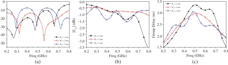
The effects of the width of the open stub, W1, on |S11|, |S21|, and group delay of the proposed
DDL are shown in Figs. 3(a)–(c). When W1 varies from 1 mm to 3 mm with a step width of 1 mm,
both |S11|and |S21|first become better and then worse, while the proposed DDL shows the maximum
group delay time at the center frequency of 500 MHz when w1 = 1 mm. The reason can be explained
as that the mutual coupling between the open stubs and the complementary slot lines is changed with the variation of W1.
Figure 4 shows the effects of various widths of the main microstrip transmission line,w0, on|S11|,
|S21|, and group delay. When w0 varies from 0.9 mm to 2.9 mm with a step width, |S11|, |S21|, and
group delay have obvious variations. The reason is that the variation of width changes the characteristic impedance of the main microstrip transmission line.
(a) (b) (c)
0.2 0.4 0.6 0.8 Freq (GHz)
0.3 0.5 0.7 0.2 0.4 0.6 0.8
Freq (GHz)
0.3 0.5 0.7 0.2 0.4 0.6 0.8
Freq (GHz) 0.3 0.5 0.7 0 -10 -20 -30 -40 -50 | S | (dB) 11 | S | (dB) 21 0.0 -0.5 -1.0 -1.5 -2.0 -2.5 -3.0 -3.5 3.5 3.0 2.5 2.0 1.5
Group Delay (ns)
W = 2 mm
W = 3 mm
W 1= 1 mm
1 1
W = 2 mm
W = 3 mm
W 1= 1 mm
1 1
W = 2 mm
W = 3 mm
W 1= 1 mm
1 1
Figure 3. Simulated |S11|,|S21|and group delay with the variation of W1. (a)|S11|, (b)|S21|and (c)
group delay.
(a) (b) (c)
0.2 0.4 0.6 0.8
Freq (GHz)
0.3 0.5 0.7 0.2 0.4 0.6 0.8
Freq (GHz)
0.3 0.5 0.7 0.2 0.4 0.6 0.8
Freq (GHz)
0.3 0.5 0.7
0 -10 -20 -30 -40 -50 | S | (dB) 11 | S | (dB) 21 0.0 -0.5 -1.0 -1.5 -2.0 -2.5 3.5 3.0 2.5 2.0 1.5
Group Delay (ns)
-60
W = 1.9 mm
W = 2.9 mm
W 0= 0.9 mm
0 0
W = 1.9 mm
W = 2.9 mm
W 0= 0.9 mm
0 0
W = 1.9 mm
W = 2.9 mm
W 0= 0.9 mm
0 0
Figure 4. Simulated |S11|,|S21|and group delay with the variation of W0. (a)|S11|, (b)|S21|and (c)
4. RESULTS AND DISCUSSION
To verify the performance of the proposed DDL, the prototype with optimized parameters is fabricated and shown in Fig. 5. The group delay is measured using the vector network analyzer of R&S ZNB20, and the simulated and measured curves are depicted in Fig. 6. It can be observed that the measured results show good corroborations with the simulated ones. The measured peak delay time is 3.2 ns at the frequency of 534 MHz.
(a) (b)
Figure 5. Photograph of the proposed DDL, (a) top view, (b) bottom view.
Figure 6. Simulated and measured group delay of the proposed DDL.
Figure 7. Simulated and measuredSparameters of the proposed DDL.
The S-parameters of the prototype are measured, and Fig. 7 gives the measured and simulated S-parameters of the proposed DDL. It can be observed that the measured results agree well with the simulated ones. The |S11| are less than −10 dB in the 200–800 MHz band, and its lowest value can
reach −35 dB. The |S21| are close to 0 dB, and the measured maximum insertion loss is 1.68 dB at
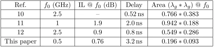
electric size without compromising the performance, which is only 6.2%, 10.3%, and 11.6% in area compared with the ones in [10, 11] and [12], respectively.
Table 1. Comparison of the DDL electrical size and performance between this and other recently published works.
Ref. f0 (GHz) IL @f0 (dB) Delay Area (λg∗λg) @f0
10 2.5 – 0.52 ns 0.766∗0.383
11 1 1.9 2.0 ns 0.942∗0.188
12 2.5 0.9 0.8 ns 0.549∗0.286
This paper 0.5 0.76 3.2 ns 0.196∗0.093
5. CONCLUSION
A compact DDL with microstrip line technology has been obtained in this letter. The required length of the complementary slot line in the proposed DDL is reduced approximately from λg/2 to λg/4 and hence significantly decreases its required area. According to the measurement results, the insertion loss, group delay, and element area have obvious advantages compared with the existing DDL, which has promising application in phase array elements and signal processing.
ACKNOWLEDGMENT
This work was supported by the Natural Science Foundation of Fujian Province of China (2019J01638) and the Science and Technology Project Plan of Fuzhou of China (2018-G-89).
REFERENCES
1. Gupta, S., A. Parsa, E. Perret, R. V. Snyder, R. J. Wenzel, and C. Caloz, “Group-delay engineering noncommensurate transmission line all-pass network for analog signal processing,” IEEE Trans. Microw. Theory Tech., Vol. 58, No. 9, 2392–2407, 2010.
2. Nikfal, B., S. Gupta, and C. Caloz, “Increased group delay slope loop system for enhanced-resolution analog signal processing,”IEEE Trans. Microw. Theory Tech., Vol. 59, No. 6, 1622–1628, 2011.
3. Keerthan, P., R. Kumar, and K. J. Vinoy, “A novel all-pass network implementation for improved group delay performance,”IEEE Microw. Wireless Comp. Lett., Vol. 26, No. 10, 804–806, 2016. 4. Kaviani D., S., G. H. Askari, R. Safian, and H. Mir-Mohammad Sadeghi, “Design and analysis of
a tunable microwave photonic delay line in X band,”2017 Progress In Electromagnetics Research Symposium — Spring (PIERS), 1138–1144, St Petersburg, Russia, May 22–25, 2017.
5. Bo, X., K. Anthony, and B. A. Alyssa, “A novel on-chip active dispersive delay line (DDL) for analog signal processing,” IEEE Microw. Wireless Comp. Lett., Vol. 20, No. 10, 584–586, 2010. 6. Zhang, J.-J. and J. Yao, “Broadband microwave signal processing based on photonic dispersive
delay lines,” IEEE Trans. Microw. Theory Tech., Vol. 65, No. 5, 1891–1902, 2017.
7. Lujambio, A., I. Arnedo, M. Chudzik, I. Arregui, T. Lopetegi, and M. A. G. Laso, “Dispersive delay line with effective transmission-type operation in coupled-line technology,” IEEE Microw. Wireless Comp. Lett., Vol. 21, No. 9, 459–461, 2011.
9. Zhang, Q., J. Bandler, and C. Caloz, “Design of dispersive delay structures (DDSs) formed by coupled C-sections using predistortion with space mapping,” IEEE Trans. Microw. Theory Tech., Vol. 61, No. 12, 4040–4051, 2013.
10. Mandal, M. K., D. Deslandes, and K. Wu, “Complementary microstrip slot stub configuration for group delay engineering,”IEEE Microw. Wireless Comp. Lett., Vol. 22, No. 8, 388–390, 2012. 11. Hsue, C.-W. and Y.-W. Chang, “Dispersive delay lines using microstrip technology,” Journal of
Engineering, 406–414, 2016.