A Dual-Layer Microstrip Patch Antenna with Stub Designed
by Simulated Annealing Algorithm for Circular Polarization
Li Guo* and Zhiqiang Yao
Abstract—In this paper, a design method that employs simulated annealing (SA) algorithm to create stub structure of a dual-layer microstrip patch antenna for circular polarization is presented. Firstly, based on established controls of SA algorithm, a series of stub structures have been created automatically on the stacked parasitic element — (Split Ring Resonator) SRR of antenna. The desired stub structure is chosen according to the generation of orthogonal modes that produce circular polarization through the electromagnetic coupling to the driven patch with an SRR-shaped slot. Then, a dual-layer microstrip patch antenna with a Z-shaped stub and left-hand circularly polarized (LHCP) characteristic is obtained by employing the assisted design. The designed antenna is simulated, optimized, fabricated, and measured. The results show that the microstrip patch antenna with Z-shaped stub has a simulated minimum axial ratio of 1.64 dB at 2.4 GHz, and the measured peak gain can be up to 5.87 dBi.
1. INTRODUCTION
Circularly polarized (CP) antennas are used widely in modern wireless communication systems, since they can aid in reduction of multipath effects and making the orientation between transmitting and receiving antennas flexible. However, sometimes the design process of CP antennas is arduous due to multi-objective solutions with the need of meeting desired or high requirements. Using optimization/evolutionary algorithms for the design of circular polarization can lighten the design process and has received much attention [1, 2]. Amongst CP antennas, single-feed multilayer microstrip patch antennas are much preferred due to their simple feeding structures [3]. In addition, by stacking parasitic or multilayer structures and employing electromagnetic coupling, high CP performances can be realized [4]. For such antennas, generally, perturbation structures need to be applied and are vital for CP radiation. Thus, to reduce design complexity, one can use optimization algorithms to only design the perturbation structure of these antennas for circular polarization. The applications behind these CP antennas include mobile communications [5], satellite communications, wireless sensor networks [6], amongst others.
As for designing single-feed CP multilayer microstrip patch antennas, the excitation of two orthogonal modes with equal amplitude and 90◦ phase difference is challenging in limited antenna geometry. Different from this, another approach needs two separate orthogonal feeds to achieve circular polarization. The radiation patch for generating circular polarization can have various shapes, such as rectangular, triangular, circular, and square-ring shapes. Generally, the patches need to be truncated, slotted or load stubs to introduce perturbations. Also, circular polarization can be realized by stacking structures [7], asymmetrical feeding, etc. When loading stubs, the functions for stubs are to introduce or excite a loaded mode and to tune the phase difference of orthogonal modes to be 90◦ [8]. However, majority of stubs are loaded on the driven patch or feeding layer, and little research work focuses on loading a stub on the stacked structure for generating orthogonal modes through electromagnetic
Received 18 July 2019, Accepted 5 September 2019, Scheduled 29 September 2019
* Corresponding author: Li Guo (guoli [email protected]).
156 Guo and Yao
coupling [9]. In addition, the loading location and shape of stubs are difficultly determined, or they are obtained with the need of amounts of human operations. Using optimization/evolutionary algorithms to design the stub structure for circular polarization can reduce heavy workloads. The possible employed algorithms may include: genetic, particle swarm, and simulated annealing algorithms, which function by generally simulating the behaviours existing in nature [10, 11]. Apart from the designs mentioned above, these algorithms have been successfully applied to the optimization of various antennas, such as wire, single-layer patch [12], and array antennas [13]. However, it is usually difficult to create/place structures using optimization/evolutionary algorithms for attaining desired performances [14]. Generally, algorithms are applied combining certain antenna characteristics for these designs [15]. In particular, stub structures on the stacked element can be designed by using algorithms and can be loaded to excite the orthogonal modes of circular polarization by employing or enhancing electromagnetic coupling. Amongst available algorithms, simulated annealing algorithm (SA) is a simple tool and has advantages in finding the hidden global minimum. It has been utilized in several antenna designs to solve multiobjective and global antenna optimization problems [16].
In this paper, a dual-layer microstrip patch antenna with a Z-shaped stub structure has been designed by employing SA algorithm which is dedicated to the creation of stub structures on a stacked SRR for circular polarization. In this regard, HFSS and MATLAB software package are used for co-simulation to create the design, for which firstly, the stub structures are generated in terms of placement of a set of discrete small rectangular sheets. Then, they are united with the stacked SRR in further optimization process. By integrating these innovations in the design, a dual-layer microstrip patch antenna with a Z-shaped stub is produced with CP property. The Z-shaped stub is used to generate orthogonal modes which result in CP radiation. The remaining parts of this paper are arranged as follows. Section 2 presents the procedure for antenna design combining the SA and resulting stub structures. Section 3 illustrates an optimized CP microstrip patch antenna and its corresponding characteristics. The conclusion is presented in Section 4.
2. ANTENNA DESIGN PROCESS 2.1. Design Methodology Combining SA
In the design process, an initial dual-layer microstrip patch antenna is first constructed following the utilization of algorithm for further design, and SA control is an important consideration for the final antenna geometry, which is dedicated to creating stub structures. Despite the general deployment of distinction optimization algorithms for optimizing antenna structures, this paper presents solutions for constructing structures on a stacked parasitic element of a microstrip patch antenna. This design is based on an original dual-layer microstrip patch antenna with co-simulation of HFSS and MATLAB. For positively exploiting the electromagnetic coupling between stacked layers of the microstrip patch antenna, two layers of substrate are employed for the designed antenna and are then spaced by an air gap layer. Furthermore, the stub structure is built on the parasitic element of the upper layer to achieve a desired impact on the driven patch and the entire antenna. A square driven patch is placed on the lower substrate, and an SRR-shaped slot is etched into it. In addition, a stacked SRR (SSRR) is placed on top of the upper substrate with its split direction facing opposite to the split of the lower SRR-shaped slot. To achieve broadband and different polarizations, the desirable stub structures are generated in a step-by-step process along the split of the SSRR. These are composed of a sequence of small rectangular conducting sheets which are selectively placed, under the control of SA. The operation steps involved are elaborated as follows.
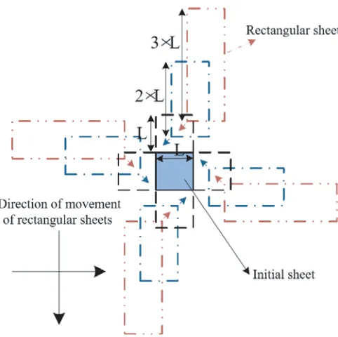
Figure 1. Diagram of the placement process of the small rectangular sheets.
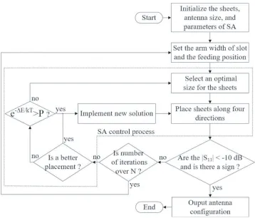
first and second resonance frequency, and frequency corresponding to the peak |S11| that lies in the previous two frequencies, are recorded to determine an optimal size for the placed small rectangular sheets. In addition, if three resonance frequencies appear in the placement process, then it gives a message to represent three possible resonant modes produced with the sheets placed in the near area. Per the criterion for optimal size, at the middle frequency, |S11|is the lowest among the stored values of the middle frequency. Fourth, a set of small rectangular sheets with optimum size are placed in an adding-and-deleting manner along all four edges of the sheet selectively before determining the following optimal sheet placement. Note that for every placement, |S11|is calculated. Fifth, if the recorded value of |S11| at the three frequencies is below −10 dB, and a message representing three resonant modes appears, then the desired stub structure is generated, marking the end of the design process. However, if the number of iterations exceeds the value ofN, then arm widths of the SRR-shaped slot and feeding position are reset. If the number of iterations is notN, then an annealing process is carried out involving probability judgment and a possible redoing of size selection for sheets which is done in step three, as required. Subsequently, SA controls the main convergence process. In addition, it is critical to set the arm width of SRR-shaped slot and feeding position as it is imperative to the overall design — if done properly, only a few iterations are needed to achieve the desired antenna design. A complete flowchart for these steps is shown in Figure 2.
In optimization process, the design is directed by calculating the|S11|only at the first and second resonance frequencies and at the peak point between the former two frequencies but not for the third one. The reason behind this is to firstly reduce program complexity, and, secondly, for matching the impedance of third resonance with the former two ones since it has a low mutual coupling and can be adjusted through further optimization. Another point worth mentioning is to place the small rectangular sheets to obtain the desired stub structures while using the random search algorithm, as it is highly difficult to converge it to target state even if it undergoes a number of dimension adjustments.
A critical part of the SA algorithm is the annealing process, which guides the convergence, as the current temperatureTn is decreased step by step. The geometric annealing process can be represented as [10, 13]:
Tn=αT0 (1)
158 Guo and Yao
Figure 2. Flowchart of design procedure. In the formula: ΔE represents the energy change related to the calculated|S11|,T is the current temperature, kis the Boltzman’s constant, andP is a random probability.
2.2. Antenna and Stub Structures
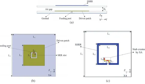
Initial antenna geometry comprising stub created by SA is presented in Figure 3. In this design, the stub consists of a set of discretely-placed, small rectangular sheets. The substrates used employ Rogers 4350B material (r = 4.38, tanδ = 0.0037, at the frequency of 10 GHz). The thicknesses for lower and upper substrates are 1.5 mm and 1 mm, respectively. The whole dimension of the antenna is 0.48λ0×0.48λ0×0.056λ0, where λ0 is the free-space wavelength at the center frequency. A set of discretely-placed small rectangular sheets constitute a stub with a certain shape, such as a Z-shaped stub, which works on positively obtaining desired antenna performances.
After a series of trial-and-correction steps, three stub structures are created, namely Z-, L-, and step-shaped stubs, as shown in Figure 4. |S11| versus frequency curves corresponding to these stubs have also been provided. The Z-shaped stub is created in terms of one initial placed sheet, while the L- and step-shaped stubs are created in terms of four. In addition, the step-shaped stub is obtained for the |S11| value −10 dB<|S11|< −9 dB in the fifth step of the design procedure. As evident from Figure 4, there are three combined resonant peaks that form a wide 10-dB (|S11|<−10 dB) impedance bandwidth. The rectangular patch, SRR-shaped slot, and SSRR induce three resonances. The creation and use of stubs makes it possible to combine the resonances in a low mutual coupling state. Note that there is a slight difference in size for the lower patch and feeding position of the three resulting antennas because of size resetting that occurs in the design procedure.
Z-(a)
(b) (c)
Figure 3. Geometry of the designed dual-layer microstrip patch antenna: (a) lateral view; (b) lower layer; (c) upper layer. The labelled dimensions are listed as follows: L1 = 60 mm, L2 = 29.5 mm,
L3 = 28 mm, L4 = 24 mm, L5 = 8 mm, L6 = 2 mm, L7 = 4 mm, L8 = 6 mm,L9 = 3 mm,d= 3.5 mm, and H1= 4.5 mm.
Figure 4. Reflection coefficients of the three designed dual-layer microstrip patch antennas with Z-, L-, and step-shaped discrete stub, respectively, along with the corresponding stub structures.
160 Guo and Yao
3. CP ANTENNA AND CHARACTERISTICS 3.1. Optimized Antenna and Reflection Coefficients
In terms of the original antennas previously created using different discrete stub structures, further optimizations are conducted by combining all the discrete sheets and by slightly adjusting SSRR and antenna dimensions for CP performance. Considering the two dual-layer microstrip patch antennas with step- and L-shaped stubs, respectively, to have similar performances, both are linearly polarized antennas with comparable impedance bandwidth and radiation pattern, and they are not discussed here for the sake of brevity. The dual-layer microstrip patch antenna with Z-shaped stub exhibits CP performance, thus, further analysis for it is taken into account, and its optimized configuration is shown in Figure 5. Sizes of its parts are correspondingly listed. Its CP characteristics will be validated in the following sections.
Figure 5. Optimized geometry of the proposed microstrip patch antenna. Partial sizes of antenna are listed as follows (unit: mm): L1 = 60, L2 = 28.1,
L5 = 8.8, L6 = 2.4, L7 = 4.5, L8 = 6.1,
L9 = 1.7, d = 3.4, and the thickness of the air gap isH1= 4.6.
Figure 6. Reflection coefficients of the proposed microstrip patch antenna with Z-shaped stub and the reference antenna without stub.
(a) (b)
Figure 7. Simulated E-field distributions of the proposed microstrip patch antenna at the second and third resonance frequencies: (a) at 2.4 GHz, (b) at 2.456 GHz.
3.2. Operating Principle of CP Antenna
Figure 7 shows simulated E-field distributions of the proposed microstrip patch antenna at the second and third resonance frequencies: 2.4 and 2.456 GHz. As shown from Figures 7(a) and (b), the maximum
E-fields of the two distributions are on the diagonal lines of the patches and orthogonal to each other. Based on this characteristic, when the corresponding two resonant modes are generated with equal amplitude and 90◦ phase difference, a CP microstrip patch antenna will be produced. It should be mentioned that when the designed CP antenna unloads the Z-shaped stub, the maximum E-fields are not orthogonal. This demonstrates that the Z-shaped stub can be used to introduce orthogonal modes; also, by tuning the amplitude and phase of the orthogonal modes, a circular polarization can be achieved. Because the resonance frequency of the 45◦-polarized E-field is lower than the resonance frequency of the 135◦-polarized E-field, and the phase of the 45◦-polarized E-field is faster than the phase of the 135◦-polarized E-field by 90◦, the proposed microstrip patch antenna exhibits left-handed CP (LHCP) [7].
3.3. AR
162 Guo and Yao
(a) (b)
Figure 8. Impacts of different lengths of the terminal strip of the Z-shaped stub on the reflection coefficient (|S11|) and axial ratio (AR) of the proposed microstrip patch antenna. (a) |S11|, (b) AR.
Figure 9. Measured AR curve of the proposed (LHCP) microstrip patch antenna and simulated ones of the LHCP and RHCP antenna (the RHCP antenna considered here is that the Z-shaped stub is reversed and connected to the other split end of the SSRR).
3.4. Radiation Patterns
(a) (b)
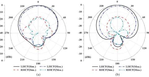
Figure 10. Simulated and measured two-dimensional radiation patterns of the proposed (LHCP) microstrip patch antenna. The observed frequencies of simulation and measurement are at 2.4 and 2.465 GHz, respectively. (a) xz plane, (b) yz plane.
4. CONCLUSION
A dual-layer microstrip patch antenna with a Z-shaped stub is designed by employing SA which aims to create stub structure for circular polarization. The design process based on SA is effectively implemented by the co-simulation of HFSS and MATLAB. The Z-shaped stub is generated on the SSRR of the antenna and results in two orthogonal modes through the electromagnetic coupling to the driven patch to achieve circular polarization. The resulting dual-layer microstrip patch antenna with a Z-shaped stub is LHCP with a narrow AR bandwidth. Simulated and measured results validate the feasibility of the CP design.
ACKNOWLEDGMENT
This work was supported in part by the Key Research Project of Hunan Province under Grant 2016JC2021, and in part by the Starting Research Fund Project of Xiangtan University under Grant 19QDZ16.
REFERENCES
1. Tseng, L. Y. and T. Y. Han, “An evolutionary design method using genetic local search algorithm to obtain broad/dual-band characteristics for circular polarization slot antennas,” IEEE Trans. Antennas Propag., Vol. 58, No. 5, 1449–1456, 2010.
2. Diego, F. M., S. S. Eduardo, and C. N. Daniel, “Circularly polarised rectangular microstrip antenna design with arbitrary input impedance,”IET Microwaves Antennas Propag., Vol. 12, No. 9, 1532– 1540, 2018.
164 Guo and Yao
4. Liu, Z. X., L. Zhu, and X. Zhang, “A low-profile and high-gain CP patch antenna with improved AR bandwidth via perturbed ring resonator,”IEEE Antennas Wirel. Propag. Lett., Vol. 18, No. 2, 397–401, 2019.
5. Hanieh, A., A. Abdolali, C. Alessandra, M. Diego, M. Rashid, and M. Pedram, “ANN-based design of a versatile millimetrewave slotted patch multi-antenna configuration for 5G scenarios,” IET Microwaves Antennas Propag., Vol. 11, No. 9, 1288–1295, 2017.
6. Yao, Z., J. Huang, S. Wang, and R. Ruby, “Efficient local optimisation-based approach for non-convex and non-smooth source localisation problems,” IET Radar, Sonar & Navigation, Vol. 11, No. 7, 1051–1054, 2017.
7. Seo, D. C. and Y. Sung, “Stacked open-loop square ring antenna for circular polarization operation,” IEEE Antennas Wirel. Propag. Lett., Vol. 14, 835–838, 2015.
8. Sung, Y., “Stub-loaded square-ring antenna for circular polarization applications,” Journal of Electromagnetic Waves and Applications, Vol. 30, No. 11, 1465–1473, 2016.
9. Sharma, V., B. Sharma, V. K. Saxena, K. B. Sharma, M. M. Sharma, and D. Bhatnagar, “Circularly polarized stacked square patch microstrip antenna with tuning stubs,” Indian Antenna Week, Kolkata, India, December 18–22, 2011.
10. Coleman, C. M., E. J. Rothwell, and J. E. Ross, “Investigation of simulated annealing, ant-colony optimization, and genetic algorithms for self-structuring antennas,”IEEE Trans. Antennas Propag., Vol. 52, No. 4, 1007–1014, 2004.
11. Deb, A., J. S. Roy, and B. Gupta, “Performance comparison of differential evolution, particle swarm optimization and genetic algorithm in the design of circularly polarized microstrip antennas,”IEEE Trans. Antennas Propag., Vol. 62, No. 8, 3920–3928, 2014.
12. Chang, L., C. Liao, W. Lin, L.-L. Chen, and X. Zheng, “A hybrid method based on differential evolution and continuous ant colony optimization and its application on wideband antenna design,” Progress In Electromagnetics Research, Vol. 122, 105–108, 2012.
13. Rattan, M., M. S. Patterh, and B. S. Sohi, “Optimization of circular antenna arrays of isotropic radiators using simulated annealing,”Int. J. Microw. Wirel. Technol., Vol. 1, No. 5, 441–446, 2009. 14. Jauhri, A., J. D. Lohn, and D. S. Linden, “A comparison of antenna placement algorithms,”
Companion Publ. Genet. Evol. Comput. Conf., Vancouver, BC, Canada, July 12–16, 2014.
15. Abri, M., N. Boukli-Hacene, and F. T. Bendimerad, “Application of the simulated annealing to the synthesis of ring printed antennas arrays,”Ann. Telecommun., Vol. 60, Nos. 11–12, 1422–1438, 2005.