processing digital filters on FPGA
Qingfeng Jing
1*, Yujia Li
1and Jincheng Tong
2Abstract
Multi-rate signal processing, an important part of the design of a digital frequency converter, is realized mainly based on interpolation and decimation, which match the sampling rate between the baseband and high-frequency processing side, especially in down conversion. However, the design of a digital filter is important for realizing multi-rate interpolation and decimation, which is highlighted in this paper. To analyze the digital filter performance in multi-rate signal processing, the ordinary finite impulse response (FIR) filter and more efficient digital filter are discussed respectively. The ordinary FIR filters use a Hamming window to design, while a more efficient digital filter includes a cascaded integrate comb (CIC) and half-band filter. Sampling rate transformation factor is 12 in this design, which is cascaded by three stages. Each stage corresponding to the conversion factor is 3, 2, and 2. Both of these design methods are implemented on the FPGA development board. The hardware resource occupancy and the error rate of the signal amplitude in decimation show that the efficient digital filter is superior to the digital filter designed by the Hamming window in the real-time processing.
Keywords:Multi-rate signal processing, Decimation, Hamming window FIR filter, CIC, Half-band filter, FPGA
1 Introduction
Multi-rate signal processing is the key technology to realize the digital frequency converter. In a general com-munication system, the rate of the baseband signal is often much lower than that of the intermediate fre-quency (IF) signal; in order to match the sampling rate of both sides, there is no doubt that the sampling rate of the former increases, which is equivalent to the increase in the number of sampling points. While in the recep-tion process, signals from an analog to digital converter (ADC) with a higher rate are difficult to provide directly to processors for processing; as a result, extraction is considered to decrease the sampling rate. In other words, the discrete sampled signal is resampled, and ul-timately, the signal frequency will be down to the appro-priate point for data recovery. So interpolation and extraction is not only the basis of multi-rate signal pro-cessing, but also an important theoretical support for digital inverter design [1].
As the functional requirements of the system become more and more diversified, the function of the circuit module in the design becomes more and more compli-cated, and the higher processing speed of the chip is of great need. In other words, traditional analog circuits cannot meet the whole design demands. So those large-scale integrated devices, such as FPGA and DSP as high-speed signal processors, have been vigorously de-veloped and promoted, which is characterized by the use of digital or software to replace the analog circuit [2]. At present, most of the transceivers include baseband signal processing, digital frequency conversion, and analog conversion. Analog frequency conversion aims at mov-ing high-frequency analog signal to the appropriate IF, which can reduce the restrictions of key devices such as AD/DA, and digital frequency conversion is prone to get a lower rate baseband signal [3].
This paper is divided into four parts: Section 1 tells
about multi-rate signal processing in the digital
frequency conversion design and further introduces its development status quo; finally, article structure is also explained. Section 2 mentions two different digital filter designs in multi-rate signal processing, including ordin-ary FIR filter and CIC, half-band filter as more efficient
* Correspondence:[email protected]
1College of Astronautics, Nanjing University of Aeronautics and Astronautics, Nanjing 210019, Jiangsu, People’s Republic of China
Full list of author information is available at the end of the article
digital filters, and provides their design schemes. Section
3 gives the detailed implementation progress and
simu-lation results of these two digital filter designs in FPGA. Section 4 is about the conclusion of this paper. Digital down conversion is designed as an example in this paper; decimation will be discussed in the later chapters. When sampling conversion factor is somewhat large, a single-stage filter would need more filter orders than multi-stages, so a three-stage filter cascade in this design is to complete the sampling rate conversion factor of 12, and each stage of decimation factor is 3, 2, and 2. The whole design block diagram is shown in Fig.1.
2 Methods
The simulations are based on FPGA Altera Develop Board. All the simulation results are calculated by Mod-elSim and Matlab2018.
3 Two designs of digital filter in multi-rate signal processing
Multi-rate signal processing is an important technique to be discussed. It consists of interpolation and decima-tion and also the corresponding design of digital filter before extraction or after interpolation. The composition of a digital frequency converter is similar to that of the analog frequency converter, mainly including the digital mixer, numerical control oscillator (NCO), and the low-pass filter. In comparison, analog frequency
con-verter’s circuit functions are not stable enough and
greatly affected by the temperature. However, a digital frequency converter not only can guarantee the orthog-onality of IF carrier, but also conveniently modify the frequency interval and other parameters. Besides, the purpose of the sampling rate conversion is to match the rate of data processing, especially in receiver design; the frequency of the received IF signal after certain decima-tion will be reduced, thereby relieving the stress of sub-sequent data processing.
Assuming that an input signal is x(n), the sampling
rate is F= 1/T, and the input signal is full of the whole frequency, that is, −F/2≤f≤F/2, the digital angular
fre-quency ω= 2πfT. The output of sampling rate
conver-sion is y(n), and the sampling rate changes to F'= 1/T'. The process of sampling rate conversion block diagram is shown in Fig.2.
So the input and output sampling rate conversion ratio we can get is:
F=F0
¼T0
=T ¼D=L ð1Þ
whereDand Lare positive integers, since it is a linear system, and the output sample sequence is also a linear combination of input samples, which can be expressed by Eq. (2):
y mð Þ ¼ Xþ∞
n¼−∞
gmð Þ n x mðb D=Lc−nÞ ð2Þ
whenD=L= 1, it becomes a normal impulse response
of the linear system in the case of constant sampling rate as we know.
From Eq. (1), whenF>F', the sampling rate gets lower, called decimation, according to the Fourier transform; it can be seen that the decimation of the signal in the time domain is equivalent to the broadening of the frequency domain. WhileF<F', the sampling rate is rising up, called interpolation, which leads to the compression of the signal spectrum. Based on that theory, it can be known that the addition of the appropriate threshold fil-ter before decimation or affil-ter infil-terpolation can keep the spectral characteristic of the original signal. In addition, when the ratio in Eq. (1) is not a positive integer, then that is a fractional transform, which is achieved by L-times interpolation first and then the D-fold
decima-tion; the structure is shown in Fig. 3, the L-times
interpolation is on the left of the block diagram and the D-decimation is on the right.
From the above description, it can be seen that the realization of interpolation and decimation depends on the filter design. The filter is designed to meet the input and output amplitude stability and anti-spectral aliasing; what is more, filter efficiency is also an important factor needed to be considered, because it affects real-time sig-nal processing [4, 5]. Two different digital filter designs
Fig. 1Down-conversion decimation cascade block diagram
will be discussed in the following part, the ordinary digital filter using a Hamming window FIR for design will be described first, and then the more efficient digital filter, including the CIC, half-band, and CIC compensa-tion filter will be discussed after.
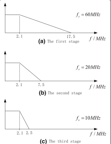
3.1 Hamming window FIR filter for decimation design From Fig. 1, it can be known that the sampling rate of each stage after filtered decimation is fk, which can be
calculated by Eq. (3):
fk¼ fk−1
Dk ;k¼1;2;3 ð3Þ
The input signal passband cutoff frequencyfpis set to
2.1 MHz in the system simulation, and in order to pre-vent the spectral aliasing caused by the spectrum exten-sion after decimation, the passband and transition zone of the last stage are designed as follows:
0≤f≤fp¼2:1MHz; fp≤f≤f3=2¼2:5MHz
ð4Þ
The methods to get passband and transition of the fol-lowing second- and first-stage filters are designed in such a way that the passband of each stage are the same, while the steepness of transition zone directly affects the order of the filter design. In line with the anti-aliasing filter de-sign, the second transition zone can be calculated.
fp≤f≤f2−f3=2¼7:5MHz ð5Þ
Similarly, the transition of first stage is
fp≤f≤f1−f3=2¼17:5MHz ð6Þ The above design gives the passband, stopband, and the output sampling rate of each stage. A filter out-of-band attenuation of not less than 55 dB is
required; from these, the filter order can be calculated by the characteristic of the Hamming window. The spe-cific formula is presented as follows:
numi¼ 6:6πffi−1=2
stop−fp
& ’
;i¼1;2;3 ð7Þ
Respectively, fp and fstop are the passband and stop-band cutoff frequency for each stage. Therefore, calculat-ing the order required for each stage of the filter, there will be more efficient digital filter design for decimation.
It can be seen that the third stage of the Hamming window digital filter whose order is up to 261, results in heavy calculations and poor real time. Therefore, a more efficient digital filter is taken into consideration. The CIC and half-band filter as more efficient filters are more common in multi-rate processing, of which the characteristics will be introduced in the following parts.
3.2 The more efficient digital filters 3.2.1 CIC filter
CIC known as cascaded integrate comb is one kind of commonly used high efficiency filters, mainly applied when the decimation factor is not the power of 2. The reason for its high efficiency is that its coefficients are 1, so it requires no multiplier. Because of this, it is often used in multi-rate transformations of high-speed signal processing.
The impulse response of the CIC filter is as follows:
Fig. 3Fractional sampling rate conversion block diagram
h nð Þ ¼ 0;1;0≤othern≤D−1
ð8Þ
where D is the decimation factor, and also represent-ing the order of CIC, the transfer function on the Z-plane is:
H zð Þ ¼ 1
1−z−1 1−z
−D
ð9Þ
Eq. (9) can be seen as a two-part cascade by the sign of multiplication; the former is an integrator and the lat-ter is a comb, which is the origin of the CIC name. The block diagram is shown in Fig.4.
Upon substitution of z=ejω into Eq. (9), we get the final amplitude frequency response:
H ejω ¼ sinðωD=2Þ
sinðω=2Þ ð10Þ
From this, the amplitude frequency curve of the CIC filter can be obtained (Fig.5).
whenD> > 1, the first side lobe amplitude is:
A¼H ejω ω¼3π
D ¼ 1
sin 3π 2D
≈
2D
3π ð11Þ
From Eq. (11), we can know the ratio of the main and side lobe amplitude is 3π/2; that is, the side lobe is only less than the main lobe with 13.46 dB. Therefore, the single CIC filter has a large side lobe amplitude, which generally cannot meet the system requirements. In order
to reduce side lobe attenuation, a multi-stage CIC filter cascade is used to aid the design; for each additional stage of the CIC filter, side lobe attenuation will be re-duced by 13.46 dB. In this design, five CIC filter cas-cades make the first side lobe attenuation up to 67 dB, which can basically meet the system requirements [6,7].
Fig. 6Half-band filter spectral characteristics
Fig. 7Down-conversion design block diagram
Fig. 8CIC filter, compensation filter, and overall frequency response
(a)
(b)
(c)
3.2.2 Half-band filter
Figure 6 shows the amplitude frequency curve of the
half-band filter. In Fig. 6, δp and δs are passband ripple
and stopband ripple, respectively, and ωp and ωA are
passband cutoff frequency and stopband cutoff fre-quency. The half-band filter has the following properties:
ωp¼π−ωA ð12Þ
δp ¼δs ð13Þ
In conjunction with the spectral characteristics of the half-band filter, it can be seen that whenδp=δsis small, as for a twofold decimation, the spectrum is twice stretched and then the 2πphase is shifted. Although the spectrum ranging fromπ/2 toωA is aliased to the signal in [ωp,π/2], the signal located in passband [0,ωp] can be recovered, so that the half-band filter can be used for twofold decimation. When the decimation factor is large and exactly the same as 2M, an M-stage half-band filter cascade can be implemented [8].
The half-band filter ensures phase linearity and the co-efficients of the filter are in even symmetry, which makes it possible to prove that all even coefficients ex-cept the center point coefficients are zero, which greatly reduces the amount of filter calculation and increases the real-time filter processing.
3.2.3 CIC compensation filter
The received signal can be recovered after being proc-essed by the digital frequency converter, which needs an appropriate design of filter parameters so that the signal waveform shape does not change significantly, but also needs to keep the amplitude of the signal within the
directly in many applications, so it is necessary to design a corresponding compensation filter so that the CIC fil-ter is flat in the pass band. The N-stage CIC filfil-ter cas-cade frequency response function can be expressed as follows (differential delayMis set to 1 as default):
H fð Þ
j j ¼ sinð Þπf
sinðπf=RÞ
N ð14Þ
wherefrepresents the sampling rate before decimation, Ris the sampling rate transform factor, andNis donated as the series of the CIC filter. The larger the parameter N, the more uneven the passband is, so an inverse fre-quency response in the passband is needed to correct this unevenness [9–11]. Thus, the response function of the CIC compensation filter can be deduced according to Eq. (14). can be approximated as an inverse Singer function.
3.2.4 Design scheme
Digital down conversion is designed as an example in this experiment, assuming that the demodulated signal is a sinusoidal two-tone signal; their frequencies are 1 MHz and 1.5 MHz. The demodulated digital sampling rate is 60 MHz, while the processing rate of back-end DSP is 5 MHz, so the sampling rate conversion factor is 12. A three-stage decimation cascade is designed to complete the down-conversion multi-rate processing. The CIC filter is put on the first stage due to its suitabil-ity for high-speed processing, which achieves threefold sampling rate conversion; the second stage is the CIC
Stopband cutoff frequency(MHz) 17.5 7.5 2.5
Filter order 42 40 261
(a)
(b)
(c)
compensation filter, which is used to reduce the non-linear effects after the CIC filter, and the factor is 2; the last stage is with a half-band filter to have two times sampling rate reduction; the whole down-conversion process is shown in Fig.7.
The compensation filter is designed by using Matlab fir2 function, and the coefficient is represented by an 18-bit fixed point; simultaneously, the passband cutoff frequency is set to 2.1 MHz, and the filter order is calcu-lated as 61. Figure8 shows the CIC filter, CIC compen-sation filter, and the whole frequency response.; it can be seen that the frequency response of the CIC is not flat in the passband before the compensation, and after the ap-propriate compensation filter design, the whole response is fairly stable so that the results of filter output do not appear to have too much fluctuations after the proper data bit truncation.
Similarly, the coefficient of the half-band filter is gen-erated using Matlab function “firhalfband” and also rep-resented by an 18-bit fixed point.
4 Implementation of two multi-rate digital filter designs
4.1 Implementation of the Hamming window digital filter on FPGA
According to the system requirements, the filter pass-band cutoff frequency is 2.1 MHz, and the out-of-pass-band attenuation is less than 50 dB. So the characteristic curve of each stage filter is shown in Fig. 9; the pass-band, stopband cutoff frequency, and sampling rate for each stage of the filter are given in the graph. On the basis of the formula of the Hamming window filter given in Section 2, the filter order of each stage can be calcu-lated as 42, 40, and 261 respectively. It can be seen that the transition band of the first-stage decimation filter is relatively narrow, so the required filter order is large, and the storage resources is also very large for the need, which greatly affects the filter processing speed. There-fore, the parameters of each filter before the decimation are shown in Table1.
According to the above design of the Hamming win-dow filter, in the hardware simulation, the input is writ-ten into the incentive test file by the way of the test input, and the output results are simulated by Model-Sim. There are 240 two’s complement data values repre-senting the two-tone signal as the test input; the output
is also the two’s complement signal after filtering. The waveform of input and output is basically the same by the simulation tool, and the peak-to-peak amplitude is also close.
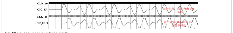
4.2 Implementation of the more efficient filter on FPGA The CIC filter requires only a small amount of adders and registers to implement the decimation process with-out the need for additional multiplier calculations. The CIC filter consists of an integrator and a differentiator; a single-stage CIC has small side-lobe attenuation and low signal to noise ratio, so a five-CIC filter cascade has been designed in this test. The block diagram of the integrator and the differential are shown in Fig.10a and b, and the five-cascade decimation of the block diagram is also shown in Fig.10c below.
The specific parameters of CIC filter is set as below (Table2).
The bit of input signal is 16 bits, and the output bit is also set to 16 bits, but the full resolution output will in-evitably exceed the effective data bits, so the final results will be generated by the decision of low-bit truncation. In the design, the CIC parameter is set, including con-version factorR= 3, cascade stageN= 5, and differential delayM= 1. The bit width of the CIC filter output is re-lated to the filter gain; for the decimation filter, the out-put gain is as follows.
G¼ðRMÞN ð16Þ
Therefore, the full resolution output bit width is:
Bout ¼ BinþN log2ðRMÞ
ð17Þ
By the calculation, a CIC decimation filter gain in this design of 243 can be obtained, that is 23.85 dB. The full-resolution output bit width is 24 bits; in order to get
Table 2CIC filter parameters
Parameter name Value
Conversion factor (R) 3
Filter order (N) 5
Differential delay (M) 1
Input bit width (bit) 16
Output bit width (bit) 16
Output rounding option Truncation
Fig. 12Twofold decimation results after compensation filter
Fig. 13Device specifications in Altera FPGA for half-band
the result with the bit width of 16 bits, the least 8 bits should be truncated. Although some error exists in this processing, fortunately, the error can be calculated by analysis [12,13].
The input signal uses a two-tone signal with frequen-cies of 1 MHz and 1.5 MHz, of which the amplitude is normalized. To prevent the amplitude calculation from overflowing in the filter processing, the normalized amp-litude is multiplied by 0.2, then the value is stored in 16-bit two’s complement. The corresponding analog for-mat output is shown in Fig.11. As can be seen from the results, after the CIC filter, the waveform did not change much, but the resolution decreased; this is because the sampling rate is reduced by three times. What is more, the CIC filter gain and output truncation produce a cer-tain error to the signal amplitude, but the error can be calculated by 243/256 = 0.9492, which is consistent with the simulation results.
The second-stage filter is the compensation filter, which mainly compensates the error caused by the non-linear effects of the CIC filter. Figure12 shows the results of the compensation filter. It can be seen that some part of the waveform has been compensated as marked. The filter coefficients are also expressed by the 18-bit fixed point, which is equivalent to amplifying the signal by 217; one bit represents the sign, and the upper 16 bits of the MSBs are intercepted and the low 19 bits of data is discarded (the maximum coefficient of the compensation filter is greater than 1, so 19 bits are used to store in the hardware actually).
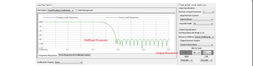
The half-band filter as the last stage whose passband cutoff frequency is set to 2.1 MHz; the ripple factor is 0.0001, using the minimum order of the design method to get the filter order of 59. Its coefficients are also rep-resented by 18-bit fixed points, and the way of output truncation is similar to that of the second-stage filter. The half-band FIR device specification in Altera cyclone IV is displayed in Fig.13.
The simulation results of the half-band filter are shown in Fig.14, and it can be seen that the signal char-acteristics in the passband are not lost.
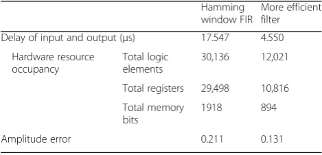
The waveform characteristics of the signal after filtering can be preserved, but the amplitude of the signal will change. Fortunately, the amplitude error of each filter can be roughly estimated, so adding a simple multiplier at the last stage can compensate for the whole filter output. Using the same simulation method to test the Hamming window digital filter, compared to the more efficient digital filter in the calculation of time, has been greatly improved. The out-put delay of the Hamming window filter is 17.547μs, while the more efficient filter is 4.550μs, simulated on the same computer, with the processor Intel i3 Core, clock 2.4 GHz.
There is a 12-time ratio between the filter input and output sampling points; the way of conventional vari-ance to determine the amplitude fluctuation after deci-mation is inappropriate, so the peak-to-peak value of the input and output is used to measure this errorη, which can be calculated as follows.
η¼jvin−voutj
vin ð
18Þ
where vin and vout are the difference of the maximum and minimum of the signal amplitude. From the simula-tion results of the design methods of two different digital filters, the amplitude range of the input signal is [−6553, 6553] and the output range after decimation by the
Hamming window filter is [−4931, 5404], while the
more efficient filter output range is [−5463, 5923], so the amplitude errors are calculated, η1= 0.211 and η2= 0.131, respectively.
The results of the two digital filter design methods are compared with the input and output delay of the filter; the hardware resource occupancy and the amplitude error of the recovery signal. The details are shown in Table3.
5 Results and discussion
In this experiment, the digital filter is designed in multi-rate signal processing in digital down-conversion process and verified its performance on FPGA. Com-pared with conventional digital filter, the more efficient filter has a great advantage on the real time and the use of hardware resources, which can improve the real-time performance of the signal processing and greatly reduce the rate of the back-end digital signal processing. It is convenient and requires relatively small resources to im-plementation, which has great application prospect.
Abbreviations
ADC:Analog to digital converter; CIC: Cascaded integrate comb; IF: Intermediate frequency; NCO: Numerical control oscillator
Funding
This research was supported by“Fundation of Graduate Innovation Center in Nanjing University of Aeronautics and Astronautics (KFJJ20181502)”.
Table 3Performance comparison of two digital filtering methods in multi-rate design
Hamming window FIR
More efficient filter
Delay of input and output (μs) 17.547 4.550
approved the final manuscript.
Competing interests
The authors declare that they have no competing interests.
Publisher’s Note
Springer Nature remains neutral with regard to jurisdictional claims in published maps and institutional affiliations.
Author details
1College of Astronautics, Nanjing University of Aeronautics and Astronautics, Nanjing 210019, Jiangsu, People’s Republic of China.2Institute of
Telecommunication Satellite, China Academy of Space Technology, Beijing 100000, People’s Republic of China.
Received: 20 June 2018 Accepted: 11 January 2019
References
1. B. Sklar,Digital communications: Fundamentals and applications, 2nd edn. (Prentice Hall, California, 2017), pp. 177–180
2. T.G. Hodgkinson, Wireless communications—The fundamentals. BT Technol. J.25(2), 11–26 (2007)
3. M. Cummings, S. Haruyama, FPGA in the software radio. IEEE Commun. Mag.37(2), 108–112 (1999)
4. J. Candy, G. Temes,Interpolation and Decimation of Digital Signals: A Tutorial ReviewProceeding of the IEEE.69(3), 300–330 (1981)
5. R.E. Crochiere, L. Rabiner, Interpolation and decimation of digital signals—A tutorial review. Proc. IEEE69(3), 300–331 (1981)
6. W. Feng, CIC filter design and analysis in multiple sampling. Mod. Electron. Technol.30(14), 18–20 (2007)
7. X. Liu, Y. Han, G. Liang, et al., inElectron devices and solid-state circuits. Design and implementation of a modified high performance and low power CIC interpolation filter.https://doi.org/10.1109/EDSSC.2011.6117685 8. Y. Liu, Q. Lin, Half-band filter principle and design—An decimation filter
with 2:1 decimation factor. PI1, 36–40 (1995)
9. E. Hogenauer, An economical class of digital filters for decimation and interpolation. IEEE Trans. Acoust. Speech Signal Process.29(2), 155–162 (1981)
10. J. Zheng, L. Ge, B. Li, Modification of CIC decimation filter and its FPGA realization. J. Inf. Eng. Univ.7(1), 57–59 (2006)
11. A.Y. Kwentus, Z. Jiang, A.N. Willson, Application of filter sharpening to cascaded integrator-comb decimation filters. IEEE Trans. Signal Process. 45(2), 457–467 (1997)