R E S E A R C H
Open Access
Acceleration of block-matching algorithms using
a custom instruction-based paradigm on a Nios II
microprocessor
Diego González
*, Guillermo Botella, Carlos García, Manuel Prieto and Francisco Tirado
Abstract
This contribution focuses on the optimization of matching-based motion estimation algorithms widely used for video coding standards using an Altera custom instruction-based paradigm and a combination of synchronous dynamic random access memory (SDRAM) with on-chip memory in Nios II processors. A complete profile of the algorithms is achieved before the optimization, which locates code leaks, and afterward, creates a custom instruction set, which is then added to the specific design, enhancing the original system. As well, every possible memory combination between on-chip memory and SDRAM has been tested to achieve the best performance. The final throughput of the complete designs are shown. This manuscript outlines a low-cost system, mapped using very large scale integration technology, which accelerates software algorithms by converting them into custom hardware logic blocks and showing the best combination between on-chip memory and SDRAM for the Nios II processor.
Keyword:Computer vision, Optical flow, MPEG compression, Block-matching algorithm, Nios II, FPGA, Custom instructions, Embedded systems
1. Introduction
Real-time motion estimation is an important task to be computed using machine vision technology and a multi-media scope. For example, one of the most time-consuming issues when computing standards with video coding and transmission has to do with the ubiquitous portable consumer electronic devices, all with multimedia capabilities, that require the efficient implementation of video coding algorithms, creating a trade-off between ac-curacy, efficiency, and power consumption. There is a pro-fusion of motion estimation algorithms and systems; many of them are frequently used in multimedia tasks and video coding standards, such as motion compensation and coding [1,2].
When considering motion estimation for multimedia purposes, the main point is to avoid the use of temporal redundancy of video data for storage and transmission [2,3]. Motion estimation for multimedia coding is achieved mostly through block-matching techniques
[4-8] that analyze the macro blocks (blocks of pixels, commonly called MBs) of the reference frame in order to estimate the closest block to the one in the current frame. Accordingly, the motion vector is defined as an offset from the current frame of MB coordinates to the MB coordinates in the reference frame. An overview of the process is shown in Figure 1.
This method of coding the processed frame with motion estimation using video is also known as inter-frame. There are several previous works regarding motion estimation hardware acceleration [9-11] and, specific-ally, block-matching algorithms [12], though none of them explore the custom instruction paradigm. Looking into block-matching techniques, three frequently used techniques can be classified: the full-search technique (FST) [4], the three-step-search technique (TSST) [13], and the two-dimensional logarithmic-search technique (2DLOG) [14].
The FST [4] matches all possible blocks within a search window in the reference frame to determine the closest block to the one fixed in the current frame (Figure 2). The closest is the one with the minimum
* Correspondence:[email protected]
Department of Computer Architecture and Automation, Complutense University, Ciudad Universitaria s/nMadrid 28040, Spain
summation of absolute differences (SAD), which is defined as:
SAD xð ;y;u;vÞ ¼X31 x¼0
X31
y¼0
Itðx;yÞ−It−1ðxþu;yþvÞ
j j;
ð1Þ
whereIt(x,y) represents the pixel value at the coordinate (x,y) in the framet, and the (u,v) is the displacement of the candidate MB. For example, for a 32 × 32 block, the FST algorithm requires 1,024 subtractions and 1,023 additions to calculate a SAD. The required number of checking blocks is (1 + 2d)2, while the search window is limited within ± d pixels, and currently, a power of two is used for it.
The TSST [13,15,16] selects nine candidate points, in-cluding the center point and eight checkpoints on the boundary of the center movement ratio search, fast for-wards to the matching point with the minimum SAD, and reduces the step size by half in each of its three steps (Figure 3). The final step stops the search process with the optimal MV so the minimum SAD can be obtained.
The 2DLOG [14] uses a pattern cross search (+) for each step until the step size is one pixel, with the initial
step size being d/4. The step size is reduced by half only when the minimum point of the previous step is at the center or the current minimum point reaches the search window boundary (Figure 4). If none of these two condi-tions is accomplished, the step size remains the same.
The organization of the paper is as follows: in Section 2, a Nios II processor overview is presented. Section 2.1 out-lines the custom instruction types. Section 2.2 discusses the different memory architectures. Section 3 shows the methodology used in this work. Section 4 shows and dis-cusses the results from the different designs. Conclusions are presented in Section 5.
2. Nios II processor
Nios II [17,18] is a 32-bit general soft-core embedded processor, which allows the acceleration of time-critical software algorithms by adding custom instructions to its instruction set. It is part of a three-member family, fast, economy, or standard, each one optimized for a specific price and performance range.
The Nios II/f Fast central processing unit (CPU) is op-timized for maximum performance [19,20]; it delivers up to 220 DMIPs of performance in the Stratix II family of field programmable gate arrays (FPGAs), placing it squarely in the advanced RISC machine (ARM) 9 [21] class of processors. This performance can be fitted to Figure 1Motivation part of the MPEG-4 scheme.
meet constraints using custom instructions, high-bandwidth switch fabric, and hardware accelerators. It supports fixed and variable cycle operations. The Nios II/e Economy CPU is optimized for the lowest cost, resulting in a smaller FPGA footprint. The Nios II/s Standard CPU delivers over 120 DMIPs while consum-ing only 930 LEs (Stratix II [22]), creatconsum-ing a balance be-tween processing performance and logic element usage.
2.1 Nios II custom instructions
A better design can be achieved with the Nios II custom instruction-based paradigm [23] by designing custom logic blocks adjacent to the arithmetic logic unit (ALU) in the processor's datapath (Figure 5) thus allowing the designer to reduce a complex sequence of standard instructions to a single instruction implemented in hardware. The Nios II processor uses GNU compiler collection (GCC) built-in functions to map custom in-structions [24]; therefore, it is feasible to use macro dir-ectly in the C or C++ application code, avoiding having to write assembly code to access the custom instruc-tions. The Nios II processor supports different types of custom instructions. Figure 6 lists the additional ports
that accommodate the different custom instruction types, where only the ports used for the specific custom instruction implementation are required.
There are four available types of custom instructions that can be used to meet each application's constraint and requirements.
The combinational type of custom instruction consists of a logic block that completes its logic function in a sin-gle clock cycle. The multi-cycle (or sequential) type of custom instruction consists of a logic block that requires two or more clock cycles to complete an operation. An extended type of custom instruction allows a single cus-tom logic block to implement several different opera-tions using an index to specify which operation the logic block will have to perform. The internal register file cus-tom instructions allow access to its own internal register file, providing the flexibility to specify whether the cus-tom instruction reads its operands from the Nios II processor's register file or from the custom instruction's own internal register file.
2.2 Memory system design for machine vision implementation
Initially, the design was implemented without using a custom instruction-based paradigm; instead, the memory types were managed in order to reach a better combin-ation to achieve a faster design. According to the Nios II specifications [17], there are four types of memory that could be used in the Nios II processor-based design: on-chip memory, external static random access memory (SRAM), flash memory, and synchronous dynamic ran-dom access memory (SDRAM). Here is a brief analysis of the advantages and disadvantages of each:
On-chip memory
On-chip memory is connected to the circuit board with-out using any external connection, because it is embed-ded inside the FPGA. As an advantage, this is the fastest type of memory that can be used in an FPGA-based em-bedded system. It allows for the pipelining of transactions, and it does not require additional circuit-board wiring, which translates to a very low cost. A disadvantage is that Figure 3Three-step-search technique: (A) first step, (B) second step, (C) third step.
it raises the volatility, which makes it lose its contents when power is disconnected, and it has limited capacity, because designed memory capacity depends only on the specific FPGA device. Considering the advantages and dis-advantages, on-chip memories are mainly utilized for stor-ing boot code or look-up tables (LUT).
External RAM
SRAM is implemented outside of FPGA and connected to it by a shared and simple bidirectional bus. As an ad-vantage, the throughput remains high, though still lower
than on-chip memories, but the storage capacity is lar-ger. However, they are more expensive per MByte than other high-capacity memory types, such as SDRAM, and they consume more board space per MByte than both SDRAM and FPGA on-chip memory, which almost consumes none.
Flash memory
Flash memory is a non-volatile memory type external to the FPGA, since FPGAs do not contain it. It has several advantages: it retains the data after the power is off; and Figure 5Nios II embedded processor. Source: Altera [13].
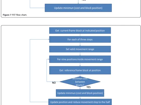
Figure 7FST flow chart.
it is low cost, erasable, and durable. One disadvantage is that it has a very high writing latency, due to the writing process requesting specific commands and bus transac-tions. Moreover, before flash memory can be written, it must be erased, and since individual words cannot be erased, entire sections of the flash must be erased as a unit. Because of their advantages and disadvantages, flash memories are mainly used to hold microprocessor boot code as well as any data, which need to be pre-served in the case of a power failure.
SDRAM
SDRAM is another type of volatile memory. It organizes the memory space in columns, rows, and banks. It is similar to SRAM, but it must be refreshed periodically
to keep its data. It requires one specific hardware con-troller, which drives the timing, address multiplexing, and refreshes every cycle. Its advantages are that it is low cost and it has a large capacity. Moreover, its power consumption is lower than SRAM. As a drawback, its required SDRAM controller occupies a major part of the interface. SDRAM latency is always greater than that of regular external SRAM or FPGA on-chip memory, al-though some types of SDRAM can achieve higher clock frequencies than SRAM. Due to its advantages and drawbacks, the devices that work with SDRAM are usu-ally low cost and high capacity.
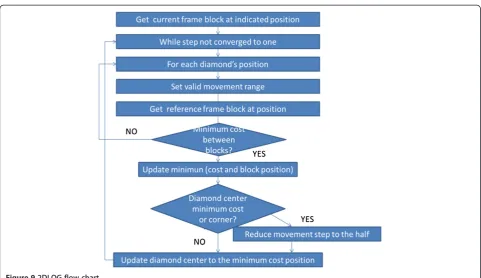
From these four types of memory, two of them were used here. Flash memory was discarded as an option due to its high latency and low capacity; additionally, Figure 92DLOG flow chart.
For each byte in source address
Copy byte from source address to destination address
non-volatile memory was not needed for this design. SRAM was discarded because of its cost per MByte, which is more expensive than SDRAM, and designing a low-cost system was of prime importance. On-chip memory was utilized, because it is the fastest memory type available on the FPGA, and it is low cost. SDRAM was also used in the design, because of its low cost and very high capacity; moreover, we needed another mem-ory, apart from the on-chip, for allocating the entire project.
3. Methodology
The methodology follows in two sections: the first sec-tion presents the parameters for the achieved designs through the use of Nios II custom instructions, and the second section presents the improvement in terms of throughput achieved through every valid and possible combinations of the on-chip and SDRAM memory into a design using the Nios II processor.
3.1 Nios II custom instructions
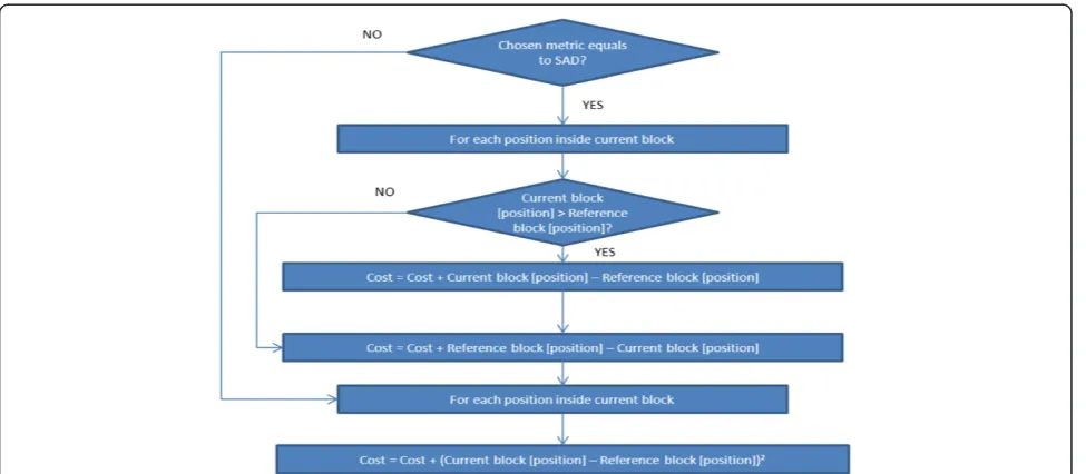
Once the different custom instruction types and the ad-vantages and disadad-vantages of each one were deter-mined, a profile of the three presented algorithms was made using the well-known code blocks tool [25]. This allowed facing up directly to the time leak point, where better performance improvement could be achieved to replace source code functions for custom instructions. For a better comprehension of the profiling, flow charts are provided in Figures 7, 8, and 9 for FST [4], TSST [13,15,16], and 2DLOG [14], respectively.
Figures 10, 11, and 12 show CopyBlock, GetBlock, and GetCost functions, respectively.
Tables 1, 2, and 3 show the profiling results accom-plished for complete executions of the motion estima-tion process, highlighting FST [4], TSST [13,15,16], and 2DLOG [14], accordingly.
By examining the profiling results, some conclusions can be made about the most appropriate part of the
For each row into block size
Call Do DMA with block row and destination address
Figure 11GetBlock flow chart.
source code to be replaced by a specific custom instruction.
The GetCost function was the first focus; moreover, as was shown in the previous tables, almost all the execu-tion time was taken. Regarding the custom instrucexecu-tion types, their weaknesses, and the GetCost function source code structure, the best approach was clearly a combina-torial custom instruction, due to its speed (only one clock cycle). Although, at first glance, it might seem a multi-cycle custom instruction should be utilized; this was impossible due to the necessary accumulated result in calculating the accumulated SAD between each pair of pixels from the selected blocks. The extended custom instruction was discarded because only one kind of operation was needed between each pair of pixels (calcu-late SAD). The internal register file custom instruction extends from the multi-cycle one, and that one was discarded for reasons previously discussed. The best can-didate was clearly monocycle custom instruction, be-cause of its low latency (only one cycle) and its easiness.
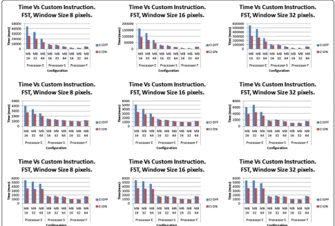
After applying the specific custom instruction used, the performance enhancement for every video-coding motion estimation algorithm in two different video se-quences is presented. Additionally, the size of each win-dow (8, 16, 32 pixels), previously explained in Figure 2, was analyzed using every possible combination with a MB size of 16, 32, 64 pixels, respectively. As well, every Nios II processor type was used in our experiments. All results for the Foreman test sequence [26] are shown in Figure 13, and all the results for the Carphone test se-quence [26] are shown in Figure 14. In Tables 4 and 5, respectively, the time spent executing time reduction for the presented results is shown for the two video se-quences for the improvement achieved for the Foreman and Carphone test benches [26].
Improvements were not dependent on the window search size; results only depended on the size of the macro block processor and algorithm; lower improvement
correlated with a higher size. For example, for the FST al-gorithm, performances moved from 10% to 55%, while for the other algorithms that were different than the pure ex-haustive full search (TSST and 2DLOG), the performance moved from 30% to 0%.
Regarding the FST algorithm, a noteworthy saving of execution time was shown; however, looking inside each processor, the greatest improvement was seen with the Nios II/e processor, around 40% of saved execution time, independent of the window search using macro block sizes of 16 and 32 pixels, although using a macro block size of 64 pixels was around 30%. Using the Nios II/s processor, the percentage of saved execution time was reduced around 20%, more or less in half; but using the Nios II/f processor, the maximum saved exe-cution time was obtained with FST, around 45% off, which was reduced when using a macro block size of 64 pixels to 10%.
Regarding 2DLOG, a noteworthy improvement in exe-cution time was shown, around 35%, using the Nios II/e processor using macro block sizes of 16 and 32 pixels, although using a macro block size of 64 pixels was around 20%. By using the Nios II/s processor, the saving was more or less 10%, which is not much compared with the saving achieved with the FST algorithm. Compared with the Nios II/f processor, the improvement was still less, around 5%.
Finally, regarding the TSST algorithm, the table shows great improvement using the Nios II/e processor, saving around 35%, as with the 2DLOG algorithm, but using the Nios II/s processor, an improvement was achieved of around 10% of the spent execution time. Finally, the Nios II/f processor still showed less improvement, which was only around 5%.
From the results, it can be determined that the obtained saving does not depend on the window size; it only depends on the macro block size and the Nios II processor type. The best improvements are achieved with the FST algorithm and with the Nios II/f processor.
3.2 Memory system design
As previously seen, the best advantages of each kind of memory can be utilized to achieve a better design. The design testing here was improved using every possible combination between the selected memories (on-chip and SDRAM) with two different video sequences. The
Table 1 FST [4] algorithm profiling
Function (FST) % Time Calls
CopyBlock 8.57 4844640
GetBlock 0.48 302790
GetCost 90.95 302691
FST approximately 0 99
Table 2 TSST [13,15,16] algorithm profiling
Function (TSST) % Time Calls
CopyBlock approximately 0 38832
GetBlock approximately 0 2427
GetCost approximately 100 2328
TSST approximately 0 99
Table 3 2DLOG [14] algorithm profiling
Function (2DLOG) % Time Calls
CopyBlock approximately 0 43280
GetBlock approximately 0 2705
GetCost approximately 100 2606
on-chip memory was chosen because it is the fastest available memory on the FPGA and SDRAM due to its large capacity and its lower cost with a good perform-ance. The window size was fixed to 32 pixels and a macro block size of 16 pixels to obtain a viable com-parison of the achieved results in each one of the tested algorithms (FST, 2DLOG, and TSST). Presented in Figures 15, 16, 17 are the combinations of memory which obtained a valid design and produced a correct program output in our testing platform, (Altera DE2 board) [27], which incorporates a chip Cyclone II EP2C35F672C6 [28].
Table 6 shows the exact memory system design achieved for each performance. Each one of the possible memories that could be chosen by the designer is shown, as well as which kind of memory (on-chip vs SDRAM) of the chosen types was used.
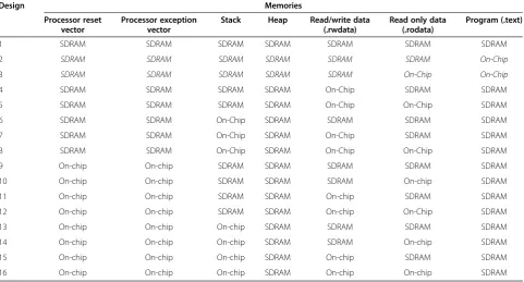
Configuration types 2 and 3 (in italics) release the bet-ter performance since program memory is allocated using on-chip memory.
The second-best configuration groups are designs 6 to 8, where the Stack is configured to be on-chip memory, and designs 13 to 16, where the main characteristic in
Stack is configured to on-chip memory. The baseline case (number 1) was considered using SDRAM in every single parameter of the microprocessor design.
4. Final results: custom instructions and memory choice
According to the two previous approaches, the embed-ded system was built by putting them together, in order to enhance the performance results. All possible mem-ory configurations were tested between on-chip and SDRAM memories in order to present the entire scope of possibilities running the three presented algorithms, including (or not) the use of the designed custom in-struction, instead of the source GetCost function in every available Nios II processor (E, S, and F). In Table 7, an overview of the FPGA used resources is presented for each one of the possible FPGA configurations, which provide all the possibilities for implementing all of the tested designs.
Figure 14Throughput obtained for each algorithm, for each processor, and for each Macro Block size.With/without using custom instruction using the GetCost function with a Carphone test bench [26].
Table 4 Achieved improvements for the Foreman test bench [26]
Technique Microprocessor
Nios II/e Nios II/s Nios II/f
MB 16 MB 32 MB 64 MB 16 MB 32 MB 64 MB 16 MB 32 MB 64
FST
8 pixels 41.72% 41.88% 32.23% 20.02 % 16.73% 15.84% 39.74% 36.22% 9.13%
16 pixels 42.58% 42.90% 33.29% 21.08% 18.86% 17.91% 50.22% 44.96% 11.15%
32 pixels 44.23% 43.21% 33.62% 21.61% 18.99% 18.42% 54.00% 53.85% 11.49%
2DLOG
8 pixels 32.35% 27.63% 20.63% 8.78% 7.25% 4.20% 6.36% 5.15% 4.13%
16 pixels 34.05% 30.05% 23.31% 11.63% 6.54% 3.94% 4.63% 8.00% 4.65%
32 pixels 35.45% 35.46% 25.61% 10.11% 10.33% 11.24% 5.50% 14.91% 5.39%
TSST
8 pixels 34.97% 33.46% 26.18% 11.24% 10.56% 8.98% 0.93% 11.21% 4.71%
16 pixels 34.67% 33.14% 26.50% 11.11% 9.44% 9.52% 4.42% 11.21% 4.12%
to the Nios‘f’processor. Inside each processor, the group of four rows were divided into two groups of two rows. The first two rows corresponded to the FPGA configur-ation without custom instruction, and the last two rows corresponded to the FPGA configuration using the cus-tom instruction. Looking at every pair of rows, it can be seen that the first one contains the chip vectors (the reset vector and the exception vector), which were allocated into the on-chip memory, and the second one allocated them into the SDRAM memory.
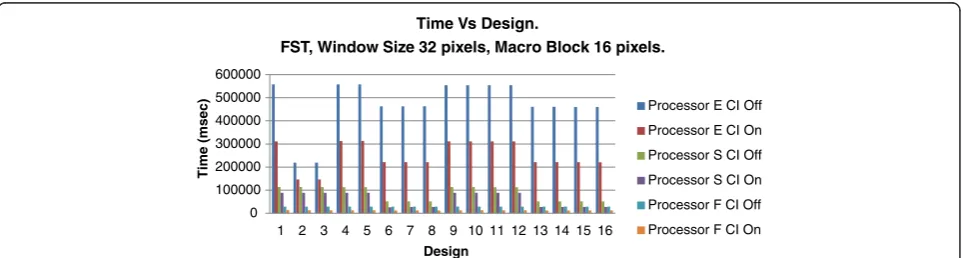
In Figures 18, 19, and 20, at-a-glance results were obtained running FST, 2DLOG, and TSST, using a macro block size of 16 pixels.
It can be seen from the charts that, as with the previ-ous eight designs, a totally descriptive set can be achieved of the memory system designs shown. For this reason, results are presented for macro block sizes of 32 and 64 pixels using only the eight previous memory system designs. In Figures 21, 22, and 23, the results obtained running FST, 2DLOG, and TSST using a macro block size of 32 pixels can be seen.
Figures 24, 25, and 26 show results obtained running FST, 2DLOG, and TSST fixing the macro block size to 64 pixels.
By examining the above charts some conclusions can be obtained regarding the tests used without custom instructions.
Regarding the Nios II processor‘e,’it can be seen that designs are divided into three families, regardless of the macro block size. The first family is formed by designs 1, 4, 5, 9, 10, 11, and 12, which have the Text program and the Stack allocated into the SDRAM memory. The second family is formed by designs 2 and 3, which are different because of the storage of the Text program in the on-chip memory, though the Stack is stored in the SDRAM. The third family is formed by designs 6, 7, 8, 13, 14, 15, and 16, which store the Text program in SDRAM but the Stack into the on-chip memory. As is evident, the second family is the fastest, followed by the third family, and finally, by the first one.
Regarding the Nios II processor ‘s,’it can be seen that designs are divided into two families, regardless of the
Table 5 Achieved Improvements for the Carphone test-bench [26]
Technique Microprocessor
Nios II/e Nios II/s Nios II/f
M B16 MB 32 MB 64 MB 16 MB 32 MB 64 MB 16 MB 32 MB 64
FST
8 pixels 42.43% 41.76% 31.72% 19.12% 17.00% 15.67% 40.39% 35.83% 9.87%
16 pixels 43.58% 42.87% 33.24% 21.02% 18.57% 17.74% 51.73% 49.03% 10.98%
32 pixels 43.91% 43.17% 33.69% 21.44% 18.99% 18.48% 56.01% 53.73% 11.53%
2DLOG
8 pixels 28.76% 28.53% 17.92% 6.79% 7.91% ~0.00% 0.92% 5.26% 1.75%
16 pixels 31.65% 30.63% 20.22% 10.44% 7.84% 5.56% 0.88% 6.06% 3.17%
32 pixels 31.05% 34.76% 26.27% 10.15% 9.36% 7.55% 5.13% 10.81% 4.94%
TSST
8 pixels 30.51% 33.65% 27.02% 9.84% 8.94% 8.54% 8.47% 10.38% 5.39%
16 pixels 30.99% 33.85% 25.61% 10.77% 10.11% 7.32% 6.72% 11.82% 5.39%
32 pixels 30.92% 33.52% 25.43% 10.42% 10.22% 7.78% 9.24% 10.19% 5.88%
0
Time Vs Memory System Design. FST, Window Size 32 pixels, Macro Block 16 pixels.
Design
macro block size. The first one is formed by designs 1, 2, 3, 4, 5, 9, 10, 11, and 12, which are different from the second family, where the Stack is stored in the SDRAM. The second family, and the fastest, is formed by designs 6, 7, 8, 13, 14, 15, and 16, where the Stack is put into the on-chip memory.
Regarding the Nios II processor‘f,’it can be seen that all the designs produce a similar throughput using macro block with sizes of 16 and 32 pixels, but by using a macro block with a size of 64 pixels, designs are di-vided into two families that correspond with the two families described when using the Nios II processor‘s.’
What follows are the uses of custom instruction and descriptions of the improvements, depending on the algorithm.
Focusing on the FST algorithm, it can be deduced that the use of custom instructions with the Nios II processor
‘e’reduce by nearly 50%, on average, the time spent by the algorithm in every family, particularly regarding the design and the macro block size, except when using a macro block size of 64 pixels, where a slightly lower re-duction was achieved, which is around 45% on average. Using the Nios II processor‘s,’the use of the custom in-struction only depends on the design family. For this reason, the first family allows a profit between 30% and 35%, but for the second family, an improvement of nearly 50% was obtained. Finally, with the use of custom instructions in the Nios II processor ‘f,’an improvement of around 55% was achieved in every design when using macro block sizes of 16 and 32 pixels; but, when using a
macro block size of 64 pixels, an improvement around 20% was achieved.
Focusing on the 2DLOG algorithm, it can be con-cluded that the use of custom instruction in the Nios II processor‘e’has an improvement rate of around 35% for the first design family, an improvement of 15% in the execution time for the second family, and for the third, a profit between 30% and 35% was obtained. Looking at the Nios II processor ‘s,’a profit between 10% and 15% was achieved using custom instructions, regardless of the particular design, although using custom instruction with the Nios II processor‘f’netted an improvement of around 10% in every design.
Focusing on the TSST algorithm, a profit between 25% and 35% was obtained using custom instruction with the Nios II processor ‘e’ for the first design family, an im-provement of 10% for the second family, and a reduction between 30% and 35% for the third family regarding the execution time. Using the Nios II processor ‘s’and cus-tom instructions, an improvement between 10% and 15% was achieved, regardless of any particular design or macro block size. Finally, using the Nios II processor‘f’ and custom instructions, a profit between 0% and 10% was obtained in every design, regardless of the fixed macro block size.
Gathering all the previous results from the experi-ments, the following conclusions were made: regarding the Nios II processor ‘e,’the fastest family is the second family, which netted a profit, on average, of nearly 75% (for FST MB 16, 32, and 64); around 60% (for 2DLOG
0
Time Vs Memory System Design.
2DLOG, Window Size 32 pixels, Macro Block 16 pixels.
Design
Figure 16Throughput obtained for each memory system design using 2DLOG.
0
Time Vs Memory System Design.
TSST, Window Size 32 pixels, Macro Block 16 pixels.
Design
MB 16, 32, and 64); and nearly 60% (for TSST MB 16, 32, and 64), depending on the algorithm. Using the Nios II processor ‘s,’ the fastest family was shown to be the second family, too, reducing the execution time, on average, nearly 75% (for FST MB 16, 32, and 64); around 20% (for 2DLOG MB 16, 32, and 64); and nearly 40% (for TSST MB 16, 32, and 64) in every algorithm. Finally, using the Nios II processor ‘f’ for the FST, an
improvement was achieved, on average, of around 55% (for FST MB 16, 32, and 64); around 40% (for 2DLOG MB 16, 32, and 64); and nearly 20% (TSST MB 16, 32, and 64) on each algorithm.
To contrast the experiments, the significant set of the memory system designs previously described (1 to 8) was tested using the Carphone test bench [26], also pre-viously described.
Table 6 Memory system design configuration
Design Memories
Processor reset vector
Processor exception vector
Stack Heap Read/write data
(.rwdata)
Read only data (.rodata)
Program (.text)
1 SDRAM SDRAM SDRAM SDRAM SDRAM SDRAM SDRAM
2 SDRAM SDRAM SDRAM SDRAM SDRAM SDRAM On-Chip
3 SDRAM SDRAM SDRAM SDRAM SDRAM On-Chip On-Chip
4 SDRAM SDRAM SDRAM SDRAM On-Chip SDRAM SDRAM
5 SDRAM SDRAM SDRAM SDRAM On-Chip On-Chip SDRAM
6 SDRAM SDRAM On-Chip SDRAM SDRAM SDRAM SDRAM
7 SDRAM SDRAM On-Chip SDRAM On-Chip SDRAM SDRAM
8 SDRAM SDRAM On-Chip SDRAM On-Chip On-Chip SDRAM
9 On-chip On-chip SDRAM SDRAM SDRAM SDRAM SDRAM
10 On-chip On-chip SDRAM SDRAM SDRAM On-chip SDRAM
11 On-chip On-chip SDRAM SDRAM On-chip SDRAM SDRAM
12 On-chip On-chip SDRAM SDRAM On-chip On-Chip SDRAM
13 On-chip On-chip On-chip SDRAM SDRAM SDRAM SDRAM
14 On-chip On-chip On-chip SDRAM SDRAM On-chip SDRAM
15 On-chip On-chip On-chip SDRAM On-chip SDRAM SDRAM
16 On-chip On-chip On-chip SDRAM On-chip On-chip SDRAM
Table 7 FPGA used resources
FPGA resources
2202(1) 1050(0) 52(52) 306,176 78 0 0 0 56 0 1,152(1) 148(0) 902(0)
2198(1) 1050(0) 52(52) 306,176 78 0 0 0 56 0 1,148(1) 148(0) 902(0)
2352(1) 1051(0) 52(52) 306,176 78 0 0 0 56 0 1,301(1) 148(0) 903(0)
2348(1) 1051(0) 52(52) 306,176 78 0 0 0 56 0 1,297(1) 146(0) 905(0)
3152(1) 1755(0) 52(52) 341,632 87 4 0 2 56 0 1,397(1) 228(0) 1,527(0)
3150(1) 1755(0) 52(52) 341,632 87 4 0 2 56 0 1,395(1) 225(0) 1,530(0)
3284(1) 1756(0) 52(52) 341,632 87 4 0 2 56 0 1,528(1) 223(0) 1,533(0)
3285(1) 1756(0) 52(52) 341,632 87 4 0 2 56 0 1,529(1) 223(0) 1,533(0)
3868(1) 2175(0) 52(52) 377,088 98 4 0 2 56 0 1,693(1) 363(0) 1,812(0)
3858(1) 2175(0) 52(52) 377,088 98 4 0 2 56 0 1,683(1) 360(0) 1,815(0)
3973(1) 2178(0) 52(52) 377,088 98 4 0 2 56 0 1,795(1) 360(0) 1,818(0)
0 100000 200000 300000 400000 500000 600000
1 2 3 4 5 6 7 8 9 10 11 12 13 14 15 16
Time (m
sec)
Design
Time Vs Design.
FST, Window Size 32 pixels, Macro Block 16 pixels.
Processor E CI Off Processor E CI On
Processor S CI Off Processor S CI On
Processor F CI Off
Processor F CI On
Figure 18Performance of final throughput (Custom instruction + Memory optimization) for FST-algorithm Nios II processor. (‘economic’,‘standard’, and‘fast’).
0 1000 2000 3000 4000 5000 6000 7000
1 2 3 4 5 6 7 8 9 10 11 12 13 14 15 16
Time (m
sec)
Design
Time Vs Design.
2DLOG, Window Size 32 pixels, Macro Block 16 pixels.
Processor E CI Off Processor E CI On
Processor S CI Off
Processor S CI On Processor F CI Off
Processor F CI On
Figure 19Performance of final throughput (Custom instruction + Memory Optimization) for 2DLOG-algorithm Nios II processor. (‘economic’,‘standard’, and‘fast’).
0 1000 2000 3000 4000 5000 6000
1 2 3 4 5 6 7 8 9 10 11 12 13 14 15 16
Time (m
sec)
Design
Time Vs Design.
TSST, Window Size 32 pixels, Macro Block 16 pixels.
Processor E CI Off
Processor E CI On Processor S CI Off
Processor S CI On Processor F CI Off
Processor F CI On
0 100000 200000 300000 400000 500000
1 2 3 4 5 6 7 8
Time (m
sec)
Design
Time Vs Design.
FST, Window Size 32 pixels, Macro Block 32 pixels.
Processor E CI Off
Processor E CI On Processor S CI Off
Processor S CI On
Processor F CI Off Processor F CI On
Figure 21Performance of final throughput (Custom instruction + Memory optimization) for FST-algorithm Nios II processor. (‘economic’,‘standard’, and‘fast’).
0 2000 4000 6000 8000
1 2 3 4 5 6 7 8
Time (m
sec)
Design
Time Vs Design.
2DLOG, Window Size 32 pixels, Macro Block 32 pixels.
Processor E CI Off
Processor E CI On Processor S CI Off
Processor S CI On
Processor F CI Off Processor F CI On
Figure 22Performance of the final throughput (Custom instruction + Memory optimization) for 2DLOG-algorithm Nios II processor. (‘economic’,‘standard’, and‘fast’).
0 1000 2000 3000 4000 5000 6000
1 2 3 4 5 6 7 8
Time (m
sec)
Design
Time Vs Design.
TSST, Window Size 32 pixels, Macro Block 32 pixels.
Processor E CI Off
Processor E CI On Processor S CI Off
Processor S CI On Processor F CI Off
Processor F CI On
0 50000 100000 150000 200000 250000 300000
1 2 3 4 5 6 7 8
Time (m
sec)
Design
Time Vs Design.
FST, Window Size 32 pixels, Macro Block 64 pixels.
Processor E CI Off Processor E CI On
Processor S CI Off
Processor S CI On Processor F CI Off
Processor F CI On
Figure 24Performance of final throughput (Custom instruction + Memory optimization) for FST-algorithm Nios II processor. (‘economic’,‘standard’, and‘fast’).
0 1000 2000 3000 4000 5000
1 2 3 4 5 6 7 8
Time (m
sec)
Design
Time Vs Design.
2DLOG, Window Size 32 pixels, Macro Block 64 pixels.
Processor E CI Off
Processor E CI On Processor S CI Off
Processor S CI On
Processor F CI Off Processor F CI On
Figure 25Performance of final throughput (Custom instruction + Memory optimization) for 2DLOG-algorithm Nios II processor. (‘economic’,‘standard’, and‘fast’).
0 1000 2000 3000 4000 5000 6000
1 2 3 4 5 6 7 8
Time (m
sec)
Design
Time Vs Design.
TSST, Window Size 32 pixels, Macro Block 64 pixels.
Processor E CI Off
Processor E CI On Processor S CI Off
Processor S CI On Processor F CI Off
Processor F CI On
0 100000 200000 300000 400000 500000 600000
1 2 3 4 5 6 7 8
Time (m
sec)
Design
Time Vs Design.
FST, Window Size 32 pixels, Macro Block 16 pixels.
Processor E CI Off Processor E CI On
Processor S CI Off
Processor S CI On Processor F CI Off
Processor F CI On
Figure 27Performance of final throughput (Custom instruction + Memory optimization) for FST-algorithm Nios II processor. (‘economic’,‘standard’, and‘fast’).
0 1000 2000 3000 4000 5000 6000 7000
1 2 3 4 5 6 7 8
Time (m
sec)
Design
Time Vs Design.
2DLOG, Window Size 32 pixels, Macro Block 16 pixels.
Processor E CI Off
Processor E CI On Processor S CI Off
Processor S CI On
Processor F CI Off Processor F CI On
Figure 28Performance of final throughput (Custom instruction + Memory optimization) for 2DLOG-algorithm Nios II processor. (‘economic’,‘standard’, and‘fast’).
0 1000 2000 3000 4000 5000 6000 7000
1 2 3 4 5 6 7 8
Time (m
sec)
Design
Time Vs Design.
TSST, Window Size 32 pixels, Macro Block 16 pixels.
Processor E CI Off
Processor E CI On Processor S CI Off
Processor S CI On Processor F CI Off
Processor F CI On
0 100000 200000 300000 400000 500000
1 2 3 4 5 6 7 8
Time (m
sec)
Design
Time Vs Design.
FST, Window Size 32 pixels, Macro Block 32 pixels.
Processor E CI Off Processor E CI On
Processor S CI Off
Processor S CI On Processor F CI Off
Processor F CI On
Figure 30Performance of final throughput (Custom instruction + Memory optimization) for full-algorithm Nios II processor. (‘economic’,‘standard’, and‘fast’).
0 1000 2000 3000 4000 5000 6000 7000
1 2 3 4 5 6 7 8
Time (m
sec)
Design
Time Vs Design.
2DLOG, Window Size 32 pixels, Macro Block 32 pixels.
Processor E CI Off Processor E CI On
Processor S CI Off
Processor S CI On Processor F CI Off
Processor F CI On
Figure 31Performance of final throughput (Custom instruction + Memory optimization) for 2DLOG-algorithm Nios II processor. (‘economic’,‘standard’, and‘fast’).
0 1000 2000 3000 4000 5000 6000
1 2 3 4 5 6 7 8
Time (m
sec)
Design
Time Vs Design.
TSST, Window Size 32 pixels, Macro Block 32 pixels.
Processor E CI Off
Processor E CI On Processor S CI Off
Processor S CI On Processor F CI Off
Processor F CI On
0 50000 100000 150000 200000 250000 300000
1 2 3 4 5 6 7 8
Time (m
sec)
Design
Time Vs Design.
FST, Window Size 32 pixels, Macro Block 64 pixels.
Processor E CI Off Processor E CI On
Processor S CI Off
Processor S CI On Processor F CI Off
Processor F CI On
Figure 33Performance of final throughput (Custom instruction + Memory optimization) for full-algorithm Nios II processor. (‘economic’,‘standard’, and‘fast’).
0 1000 2000 3000 4000 5000
1 2 3 4 5 6 7 8
Time (m
sec)
Design
Time Vs Design.
2DLOG, Window Size 32 pixels, Macro Block 64 pixels.
Processor E CI Off
Processor E CI On Processor S CI Off
Processor S CI On
Processor F CI Off Processor F CI On
Figure 34Performance of final throughput (Custom instruction + Memory optimization) for 2DLOG-algorithm Nios II processor. (‘economic’,‘standard’, and‘fast’).
0 1000 2000 3000 4000 5000
1 2 3 4 5 6 7 8
Time (m
sec)
Design
Time Vs Design.
TSST, Window Size 32 pixels, Macro Block 64 pixels.
Processor E CI Off
Processor E CI On Processor S CI Off
Processor S CI On Processor F CI Off
Processor F CI On
Figures 27, 28, and 29 show the results obtained run-ning FST, 2DLOG, and TSST fixing the macro block size to 16 pixels.
Figures 30, 31, and 32 show the obtained results run-ning FST, 2DLOG, and TSST fixing the macro block size to 32 pixels.
Finally, Figures 33, 34, and 35 show the obtained re-sults running FST, 2DLOG, and TSST by fixing the macro block size to 64 pixels.
5. Conclusions
In this paper, the problem of the acceleration motion es-timation algorithm, widely used for video coding MPEG (H.264/6), was addressed by building an FPGA-based low-cost embedded system, the Altera DE2 platform, and customizing the well-known soft-core microproces-sor Nios II. The technique developed here has been sep-arately evaluated using a custom instruction paradigm through a combinational instruction and the efficient combination of on-chip memory and SDRAM regarding the reset vector, exception vector, stack, heap, read/write data (.rwdata), read only data (.rodata), and program text (.text) in the design. A combination of two methods was then developed to build the final embedded system. With the use of custom instructions, an improvement was reached of 23%, on average, but close to a 55% im-provement, in the best case, which supposes a great amount of savings in time spent for execution. With a better use of the memory types available in the design, an improvement of 61% was achieved in the execution time. With the combination of both techniques, an im-provement of 75% was achieved against the base case.
Competing interests
The authors declare that they have no competing interests.
Acknowledgments
The authors would like to thank the Altera Company for the provided hardware and software under the University programs. The authors would like to thank Professor Uwe Meyer-Bäse from Florida State University for his help and support regarding digital signal processing with FPGAs. This work has been partially supported by Spanish Projects TIN 2008/508 and TIN 2012/32180.
Received: 15 February 2013 Accepted: 29 May 2013 Published: 16 June 2013
References
1. D Marpe, T Wiegand, GJ Sullivan, The H.264/MPEG4 advanced video coding standard and its applications. IEEE Commun Mag44, 134–143 (2006) 2. ITU-T Recommendation H.264 (draft),International standard for advanced
video coding(ITU-T, Geneva, 2003)
3. ITU-T Recommendation H.264 & ISO/IEC 14496-10 (MPEG-4) AVC,Advance Video Coding for Generic Audiovisual Services(ITU-T, Geneva, 2005) 4. J Konrad, Estimating motion in image sequences. IEEE Signal Process Mag
16, 70–91 (1999)
5. S Kappagantula, K-R Rao, Motion compensated interframes image prediction. IEEE Trans Commun33, 1011–1015 (1985)
6. C-J Kuo, C-H Yeh, S-F Odeh, Polynomial search algorithms for motion estimation, inProceedings of the 1999 IEEE International Symposium on Circuits and System (ISCAS’99), vol. 4 (Orlando, 1999), pp. 215–218
7. S Zhu, K-K Ma, A new diamond search algorithm for fast block-matching motion estimation. IEEE Trans Image Process9, 287–290 (2000) 8. S Zhu,Fast motion estimation algorithms for video coding(Nanyang
Technology University, Singapore, M.S. thesis, 1998)
9. F Ayuso, G Botella, C García, M Prieto, F Tirado, GPU-based acceleration of bio-inspired motion estimation model. Concurrency and Computation: Practice and Experience25, 1037–1056 (2013). doi:10.1002/cpe.2946 10. G Botella, A García, M Rodriguez-Alvarez, E Ros, U Meyer-Bäse, MC Molina,
Robust bioinspired architecture for optical-flow computation. IEEE Trans. VLSI Syst.18(4), 616–629 (2010)
11. C Garcia, G Botella, F Ayuso, M Prieto, F Tirado, Multi-GPU based on multicriteria optimization for motion estimation system. EURASIP JOURNAL on Advances in Signal Processing2013, 23 (2013)
12. D González, G Botella, U Meyer-Baese, C García, C Sanz, M Prieto-Matías, F Tirado, A Low, Cost Matching Motion Estimation Sensor Based on the NIOS II Microprocessor. Sensors12, 13126–13149 (2012)
13. T Koga, K Iinuma, A Hirano, Y Iijima, T Ishiguro, Motion compensated interframe coding for video conferencing, inProc. of the Nat.
Telecommunications Conference(New Orleans, LA, 1981), pp. G5.3.1–G5.3.5 14. J-R Jain, A-K Jain, Displacement measurement and its application in
interframes image coding. IEEE Trans Commun29, 1799–1808 (1981) 15. B Liu, A Zaccarin, New fast algorithms for estimation of block motion
vectors. IEEE Trans. Circuit. Syst. Video Technol.3, 148–157 (1993) 16. R Li, B Zeng, M-L Liou, A new three-step search algorithm for block motion
estimation. IEEE Trans. Circuit. Syst. Video Technol.4, 438–422 (1994) 17. Altera, Nios II processor: the world's most versatile embedded processor,
(2013). http://www.altera.com/devices/processor/nios2/ni2-index.html. Accessed 10 June 2013
18. P Chu,Embedded SoPC Design with NIOS II Processor and Examples(Wiley, Hoboken, 2012)
19. Altera, Nios II performance benchmarks, (2013). http://www.altera.com/ literature/ds/ds_nios2_perf.pdf. Accessed 10 June 2013
20. Altera, Documentation: Nios processor, (2013). http://www.altera.com/ literature/lit-nio.jsp. Accessed 10 June 2013
21. Arm, ARM: the architecture for the digital world, (2013). http://www.arm. com/products/processors/classic/arm9/. Accessed 10 June 2013 22. Altera, Stratix II FPGA: high performance with great signal integrity, (2013).
http://www.altera.com/devices/fpga/stratix-fpgas/stratix-ii/stratix-ii/st2-index. jsp. Accessed 10 June 2013
23. Altera, Hardware acceleration, (2013). http://www.altera.com/devices/ processor/nios2/benefits/performance/ni2-acceleration.html. Accessed 10 June 2013
24. Altera, Nios II custom instruction user guide, (2013). http://www.altera.com/ literature/ug/ug_nios2_custom_instruction.pdf. Accessed 10 June 2013 25. Y Mandravellos, Code::Blocks IDE, (2006). https://launchpad.net/codeblocks.
Accessed 10 June 2013
26. C Yushin, CIPR sequences, (2013). http://www.cipr.rpi.edu/resource/ sequences/. Accessed 10 June 2013
27. Altera, DE2 development and education board, (2013). http://www.altera. com/education/univ/materials/boards/de2/unv-de2-board.html. Accessed 10 Feb 2013
28. Altera, Cyclone II FPGAs at cost that rivals ASICs, (2012). http://www.altera. com/devices/fpga/cyclone2/cy2-index.jsp. Accessed 10 June 2013
doi:10.1186/1687-6180-2013-118
Cite this article as:Gonzálezet al.:Acceleration of block-matching
algorithms using a custom instruction-based paradigm on a Nios II microprocessor.EURASIP Journal on Advances in Signal Processing2013
![Figure 5 Nios II embedded processor. Source: Altera [13].](https://thumb-us.123doks.com/thumbv2/123dok_us/902895.1108941/4.595.57.541.460.717/figure-nios-ii-embedded-processor-source-altera.webp)
![Table 4 Achieved improvements for the Foreman test bench [26]](https://thumb-us.123doks.com/thumbv2/123dok_us/902895.1108941/10.595.57.540.89.424/table-achieved-improvements-foreman-test-bench.webp)
![Table 5 Achieved Improvements for the Carphone test-bench [26]](https://thumb-us.123doks.com/thumbv2/123dok_us/902895.1108941/11.595.57.549.101.308/table-achieved-improvements-carphone-test-bench.webp)