-
---
- -
G A34
-
0027
-
0
'
-
-
-
-
- - -
-
---- ----
-
----
_.-c
(~
-
-
-
GA34-0027-0
-
-
-
- - - -
- -
--
-..---
-
-
----
_ _9_
_
..
-Series/1
ii GA34-0027
First Edition (November 1976)
Changes are periodically made to the information herein; any such changes will be reported in subsequent revisions or Technical Newsletters.
Text for this manual has been prepared with the IBM Magnetic Tape Selectric® Composer.
Requests for copies of IBM publications should be made to your IBM representative or the IBM branch 0 ffice serving your locali ty .
A form for readers' comments is provided at the back of this publication. If the form has been removed, send your comments to IBM Corporation, Systems Publications, Department 27T, P.O. Box 1328, Boca Raton, Florida 33432. Comments become the property of IBM.
Contents
c
Preface v Read Status 3-14
Organization of this Book v Device Reset 3-14
Prequisite and Related Publications v Analog Input Commands 3-15
Common Commands 3-16
Chapter 1. 4982 Sensor Input/Output Analog Input Convert Commands 3-16
Unit and Attachment Feature 1-1 Diagnostic Commands 3-18
Introduction 1-1 IO Instruction Condition Codes 3-20
Unit Description 1-2 Condition After Power On Transition and Resets 3-20
Attachment Feature 1-4 Analog Output Commands 3-20
Analog Inpu t Feature 1-4 Common Commands 3-21
Analog Input Control Feature 1-4 Write Analog Output Commands 3-21
Amplifier-Multirange Feature 1-4 10 Instruction Condition Codes 3-21
Multiplexer-Solid State Feature 1-4 Condition After Power On Transition and Resets 3-21
Multiplexer-Reed Relay Feature 1-6 Digital Input/Process Interrupt Feature Commands 3-21
Analog Output Feature 1-6 Common Commands 3-22
Digital Input Features 1-6 Digital Input Commands 3-22
Digital Input/Process Interrupt-Isolated Feature 1-7 Process Interrupt Commands 3-23
Digital Input/Process Interrupt-Nonisolated Feature 1-8 Diagnostic Commands 3-24
Digital Output-Nonisolated Feature 1-8 IO Instruction Condition Codes 3-24
Configurations 1-8 Condition After Power On Transition and Resets 3-24
Sensor Input/Output Applications 1-8 Digital Output Commands 3-24
Common Commands 3-25
Chapter 2. Feature Performance Specifications 2-1 Write DO 3-25
AI Features, Solid State Multiplexer 2-2 IO Instruction Condition Codes 3-25
AI Features, Reed Relay Multiplexer 2-4 Condition After Power On Transition and Resets 3-25
('
AO Feature 2-6DI/PI Feature, Isolated 2-7
DI/PI Feature, Nonisolated 2-9
Appendix A. Analog Performance Terminology A-I
DO Feature 2-11 Appendix B. Solid State Multiplexer Low Pass
Features User Connections 2-12 Filter Selection B-1
Feature Cycle Time Samples 2-13
Index X-I
Chapter 3. Sensor Input/Output Commands 3-1
Input/Output Data Transfer Operations 3-1 Operate Input/Output Instruction 3-1 Immediate Device Control Block 3-2 Direct Program Control Operation 3-3
Input/Output Condition Codes and Status Information 3-4 Operate Input/Output Instruction Condition Code 3-6 Interrupt Condition Codes 3-6
Input/Output Status Information 3-7
Command Summary 3-8
Sensor Input/Output Unit Attachment Feature Commands 3-9
Common Commands 3-10
#.~
l_J
c
('
This publication contains the IBM Series/l 4982 Sensor Input/Output Unit Feature descriptions and the 4982 feature performance specifications necessary for the user to design a sensor I/O system application. It also contains information for programming the applications of the 4982 unit in Series/l machine language.
Introductory material necessary to understand this book is presented in the prerequisite publications listed below. In
addition, a general knowledge of sensor input/output such as contained in the IBM data processing application manual, Principles of Data Acquisition Systems, GE20-0090, is assumed.
ORGANIZATION OF THIS BOOK
This publication contains three chapters and three appendixes.
Chapter 1 introduces the IBM Series/l 4982 Sensor Input/Output Unit, its associated sensor I/O feature cards, and the Sensor Input/Output Unit Attachment Feature card. Specific topics covered are:
• Sensor Input/Output Unit Attachment Feature
• Digital Input/Process Interrupt (DI/PI)-Isolated Feature • Digital Input/Process Interrupt (DI/PI)-Nonisolated
Feature
• Digital Output (DO)-Nonisolated Feature • Analog Input (AI) Control Feature • Amplifier-Multirange Feature (AI) • Multiplexer-Solid State Feature (AI) • Multiplexer-Reed Relay Feature (AI) • Analog Output (AO) Feature
Preface
Chapter 2 describes in detail the sensor I/O unit performance specifications useful in the design of a sensor I/O subsystem application.
Chapter 3 describes the use of the sensor I/O feature machine language commands and functions.
Appendix A provides IBM definition of analog performance terminology.
Appendix B is a detailed description of the solid state multiplexer low pass filter selection.
PREQUISITE AND RELATED PUBLICATIONS
Prerequisite Series/l publications are the IBM Series/l Model 34953 Processor and Processor Features Description Manual, GA34-0022, or the IBM Sen·es/l Model 5 4955
Processor and Processor Features Description Manual, GA34-0021.
()
c
(
INTRODUCTION
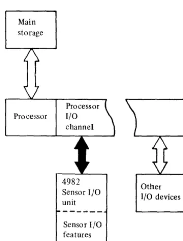
The IBM Series/l 4982 Sensor Input/Output Unit is a flexible, modular approach to attaching sensor user processes to the IBM Series/l (Figure 1-1). The 4982 sensor I/O unit attaches to the Series/l by means of the IBM 4982
Sensor Input/Output Unit Attachment Feature, a
prerequisite for the sensor I/O unit. Location of the attachment feature, which controls the transfer of information between the processor and the 4982, may be in any of the following system units:
• IBM Series/l Model 5 4955 Processor • IBM Series/l Model 3 4953 Processor
• IBM Series/l 4959 Input/Output Expansion Unit
Sensor I/O user process
Chapter 1. 4982 Sensor Input/Output Unit
and Attachment Feature
Together, the sensor I/O unit and the attachment feature provide the Series/l user with a broad base for general digital and analog I/O feature applications. Optimum use of sensor I/O feature space is attained by the flexibility of feature locations. Planned modularity allows for easy expansion of a small initial installation to a larger configuration as needs change.
IBM 4982 Sensor Input/Output Attachment Feature
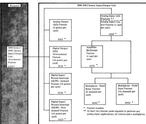
[image:8.623.141.468.299.700.2]Located near the processor in a rack enclosure, the 4982 sensor I/O unit is a subsystem of the Series/I-providing an extensive subset of the processor I/O channel for control, data transfer extensive error analysis and recovery for the sensor I/O processes.
The 4982 sensor I/O unit offers the following features:
• Analog Input
-Analog Input Control -Amplifier--Multirange -Multiplexer-Solid State -Multiplexer-Reed Relay-• Analog Output
• Digital Input/Process Interrupt-Isolated • Digital Input/Process Interrupt-Nonisolated • Digital Output-Nonisolated
UNIT DESCRIPTION
The 4982 Sensor Input/Output Unit (Figure 1-2) is a (_)
half-rack unit, equipped with the following:
• A nine card socket circuit board (eight sensor I/O feature sockets and one termination socket)
• A 3.1 m (10 ft) attachment feature cable
• Cable termination and control functions (termination card)
• A power supply
The eight feature sockets and the termination card are accessable from the rear of the unit. The termination card, which connects the 4982 to the attachment feature cable, contains termination and control logic for the unit. Located in the front section of the unit, the 4982 power supply receives input power from the individual primary power distribution panel in the 4997 Rack Enclosure.
4997 Rack Enclosure
o
Sensor I/O unit
111111111
III
1-2 GA34-0027
Sensor I/O attachment
feature-Series/1 processor (4955) _ ... _ .... with programmer console
4959 I/O expansion unit 11111111111111111111111111111111111111111111111
[]
111111111111111111111111111111111111111111111111
o
[]J0
1111111111111111111
o
[]JI
111111111111111111111111111111111111111111111111
[image:9.624.85.513.271.667.2]c
Card locations (slots) for the 4982 termination card and sensor I/O features are shown in Figure 1-3. Sensor I/O features are installed in any location and in any order, with the exception of analog input. The analog input control feature (if used) occupies card location 0, and the multirange amplifier feature (if used) occupies card location1. A multiplexer feature occupies the location adjacent to the analog input control feature or to the multirange amplifier feature. Additional multiplexer features occupy successively adjacent locations.
The attachment feature may be installed in either a 4953 or 4955 Series/1 processor or a 4959 I/O expansion unit, see Figure 1-1. The user provides the cables to connect an application to the various 4982 sensor I/O features.
4982 circuit board
Termination card for the sensor I/O unit attachment cables
The suggested user cable connector is a commercially available 56 pin connector with a protective hood. This connector requires no special tools and provides an orderly method of terminating the large number of connections required for attaching a typical user process.
Direct program control commands are used for data transfer between the processor I/O channel and the sensor I/O features. The features are individually addressed from the processor using assigned feature addresses. The sensor I/O and attachment features are extremely flexible, employing parameters variable either by programming or feature card plugging. Chapter 3 explains direct program control, feature addressing, variable parameters, and the commands used with each feature.
Sensor I/O features
Multirange amplifier feature (if used)
Analog input control feature (if used)
[image:10.624.149.481.247.458.2]ATTACHMENT FEATURE
The sensor I/O unit attachment feature logically adapts the processor I/O channel to the 4982 unit termination card. In turn, the termination card contains the logic to adapt the attachment feature to the sensor I/O features. Together, 4982 sensor I/O unit and the attachment feature furnish the IBM Series/l user with a versatile sensor I/O subsystem (Figure 1-4.)
The attachment feature performs the following
functions:
• Interprets and executes commands from the channel • Changes the I/O device address to a unique feature
address
• Provides the path for data between the processor I/O channel and the 4982
• Furnishes status information to the processor I/O channel
• Performs diagnostic functions for itself and for the 4982 termination card
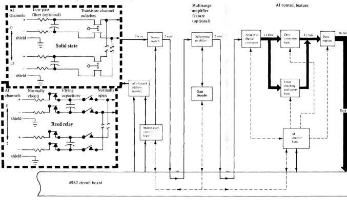
ANALOG INPUT FEATURES
Analog input (AI) features (Figure 1-5) furnish AI control,
analog-to-digital conversion (ADC), and AI signal
multiplexing for the Series/I. AI features are grouped together because at least two features are required to perform any AI application-the AI control feature and a multiplexer feature. Basically the AI control feature consists of control and voltage conversion logic. The multiplexer feature (solid state or reed relay) selects the desired AI signal for conversion to a binary value. The multirange amplifier feature (a programmable, seven range amplifier) is optional. For definition of analog terms refer to Appendix A.
Feature
Analog Input Control Feature
The AI control feature contains the following circuit logic for the AI features:
• Twelve bit (including sign bit) successive approximation ADC with an input voltage range of ±5 volts.
• Logical zero correction (reduces offset drift errors due to temperature and aging)
• Error checking and status • Control
Only one AI control feature is used in a 4982 unit.
Amplifier -Multirange Feature
The multirange amplifier feature improves measurement resolution for low amplitude AI signals (full-scale ranges of
±10 m V through -500 m V to +5V). If the multirange
amplifier feature is used, the AI features can read voltages in seven programmable ranges (see "Analog Input Commands" in Chapter 3). Only'one multirange amplifier feature is used in a 4982 unit.
Multiplexer-Solid State Feature
The solid state multiplexer feature provides the user with sixteen 2-wire analog input channels each having an input range of up to ±5V. Fast scanning and sampling rates are obtainable with this feature. This feature furnishes a program controlled means of selecting a single user input to the ADC (through the multirange amplifier if used). Solder terminals are included on the feature for user addition of low-pass filters (see Appendix B). Adding low-pass filters reduces the feature's susceptibility to high frequency electrical noise.
Analog and digital input
Analog and
digital output
Figure 1-4. Sensor I/O subsystem simplified data flow
1-4 GA34-0027
[image:11.618.119.494.490.668.2]o
,-.,
Multiplexer (solid state or reed relay)
1--- - ---
AI Low pass Transistor channel •I
channels filter (optional)I
+ ---v\/'...--... - - - ,IOI_~
• shield~
I
-=
Solid state!15
~=f ~
I
0I
.
shIeld
---:::L
I
Reed relayI
I
+~ 7
-0
I
00~
I
shield~
~
I ___
,;i _ _ _ _ _ _ _ _ _ ..
::3
AI channel address re/!Ister
Multirange amplifier feature (optional)
Analo/! to I 12 bits digital
converter
AI control feature
Zero
correction 1
al
logic
L _ _ _
I· rror checking and status logic
----'
I I I
Multiplner I I
I
control
lo~ic AI
control ___ J logic
n
[image:12.797.60.738.62.453.2]Multiplexer-Reed Relay Feature
Using the reed relay multiplexer feature provides the user with eight 2-wire analog input channels each having an input range of +SV to -SOOmV. This feature employs the
flying capacitor principle to isolate the common-mode
voltage (up to 200 volts) from the internal circuitry and to provide high common-mode rejection. The multiplexer feature furnishes a program-controlled means of selecting a single user input to the ADC (through the multirange amplifier feature, ifused).
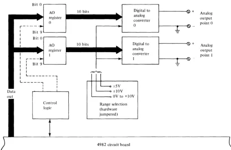
ANALOG OUTPUT FEATURE
The analog output (AD) feature (Figure 1-6) uses a digital-to-analog converter to convert a binary digital value to an analog output voltage of the corresponding value. This feature provides two points of nonisolated analog output. Each point has three selectable output voltage ranges. The ranges are selected by jumper plugs on the feature card. The range is selected when the feature is ordered, and may be changed by the user. User connections to each point are made to screw terminals.
Bit 0
I
AO 10 bits
...
register
...
0
I
r - - - - ...
I Bit 9
I
I Bit 0
I
I
10 bits
I AO
register
I
...
II
I r---~
I : Bit 9
I I I I
I
I L ________ .,
I I
...
-.
.,.
...
--..
L _____ -,
I
r=:
±5VI I
I I
Data I ±lOV
DIGITAL INPUT FEATURES
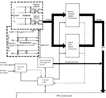
There are two versions of the digital input (DI) feature-isolated digital input/process interrupt (DI/PI) and nonisolated DI/PI (Figure 1-7). With the exception of the· input characteristics these two features are identical. The differences in input characteristics is discussed later in this chapter.
The DI/PI features are versatile, programmable features of the sensor I/O unit. These features, under program control, may be used in three separate modes:
• Processor initiated (not in response to an interrupt) • External sync interrupt initiated
• Process interrupt initiated
With processor initiated mode, the processor reads the DI register without an interrupt.
External sync interrupt initiated mode requires the feature to be armed (or enabled) for external sync. The user external sync input interrupts the processor to indicate a DI external sync operation; the Dr register is latched and available for reading. The external sync mode relieves the Series/l processor of DI polling and allows up to 16 DI register bits to be set asynchronously and read as a single group.
Digital to analog converter 0
~
Digital to analog converter I J-J('\-....
-... \.Y "" \.Y + + Analog output point 0 Analog output point Iout OV to +lOV
Control Range selection
logic (hardware
jumpered)
J
4982 circuit board~
Figure 1-6. AO feature
1-6 GA34-0027
o
\. J
[image:13.618.68.529.354.653.2]c
(
Process interrupt (PI) initiated mode requires the feature to be armed for PI. Activating any PI register latch presents a PI interrupt to the Series/l processor and indicates the PI register is available for reading. Activation of additional PI register latches will not create additional interrupts until the PI register is reset. DI diagnostic operations are also performed with the DI/PI feature.
The three program modes can be combined to provide the user with an extremely flexible DI/PI process control. Also, due to the versatile design of the DI/PI features, certain modes may be program overlapped (see Chapter 3, "Digital Input/Process Interrupt Feature Commands") .
..
-
---,
Optical I
I :
----1Ii~
...
m~j
::
IDI
points Isolated OpticalI
I
}s
+{~:~n~""'_l1l
__
I
~____
~r-
I
I
L _ _ _ _ _ _ _ _ ,
+48 V..
; 0
uvel
:="---<10 ;
It
Ret~.
i=
::
101 points Nomsolated +48 V .'
:
p~vell=
0I
Diagnostics115
==
I
I
Ref =i= ••L _ _ _
-= _ _ _ _ _ _ ....External sync ready
External sync input
External sync
~L--_ _ _ ----,
Arm, interrupt, and diagnostic latches
---,
,
,
logic
Digital Input/Process Interrupt-Isolated Feature
DI/PI isolation, achieved by photo couplers, allows the user signal source ground reference to be different from the sensor I/O unit ground reference. Improved common-mode rejection is provided with the isolated DI/PI feature. This feature accepts/only voltage level inputs (no contact sense). Each of the 16 points has both high and low level inputs.
Process interrupt register (16 latches)
Digital input register (16 latches)
ID and status bits
--,
I
I
I
I
I
I
I I
I
I
---I
I
I
I
I
I
I
I
,
I
_ _ _ _ _ _ _ _ _ _ J
[image:14.620.84.535.215.632.2]Digital Input/Process Interrupt-Nonisolated
Feature
The nonisolated DI/PI feature is similar to the isolated DI/PI feature with exception of the following:
• Ground reference for all user input points is the sensor I/O unit chassis
• A process interrupt input is sensed as a negative transition
• No common-mode voltage is allowed
• Each of the 16 input points, with high or low level capabilities, can detect either user contact closure (contact sense) or user voltage levels (voltage sense)
A +48 volts dc is supplied by the 4982 to sense the opening and closing of the user contacts in the contact sense application. The user contacts are connected directly to the input terminals.
The absence or presence of a user voltage is sensed in the voltage sense application. The user voltage is connected to the input terminals and is referenced to ground.
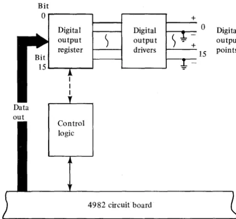
DIGITAL OUTPUT-NONISOLATED FEATURE
The nonisolated digital output (DO) feature (Figure 1-8) provides 16 points of solid state nonisolated digital output. The DO feature contains one group of 16 grounded emitter output transistors. A binary one turns the transistor on, causing a negative transition. A binary zero turns the transistor off, causing the output to go to +5.5 V dc maximum or to the user supply voltage level (whichever is larger). All 16 bits are written to the ou tpu t in parallel and latched until a new word is loaded into the DO register. The DO feature switches user loads, with a user supplied voltage, or drives TTL loads directly. User supplied voltage (a maximum of +52.8 volts dc) is referenced to processor ground. Each point is capable of shunting or switching up to 250 milliamps of current.
CONFIGURATIONS
Figure 1-9 summarizes sensor I/O feature configurations. The following are samples of different 4982 configurations, showing the flexibility of the 4982 features:
• 64 DI/PI points and 64 DO points
• 32 DI/PI points, 32 DO points, 2 AO points, and 32 solid state multiplexer channels with AI control only (single range)
• 16 DI/PI points, 16 DO points, 2 AO points, and 24 reed relay multiplexer channels with AI control and multi range amplifier
1-8 GA34-0027
Data out
Bit
0 - - - .
Bit
Digital output register
L..-_--'
15 L..---._--'
Control logic
Digital output drivers
4982 circuit board
Figure 1-8. DO feature
+
~ _ _ O
+
L - - _ -15
SENSOR INPUT/OUTPUT APPLICATIONS
Digital output points
The 4982 Sensor Input/Output Unit is used with Series/l to monitor and control the user processes. Sensors installed at equipment being monitored send digital or analog input signals to the computer. The input signals represent the status of the activity being monitored, and the computer translates the signals into meaningful data. The computer can be programmed to accept the input si.gnals on a priority basis, measure and/or record the data, check the data against predetermined standards, and return output signals to the attached equipment.
Sensor I/O can be used in many ways; for example, it can be used to monitor large numbers of manufacturing machines, to control one or more continuous or batch processes, or to monitor one or more sensor-based inputs from a test instrument. Input signals to the computer can come from analog transducers and from digital sources, such as contact closures. Computer output (both analog and digital) can control many kinds of displays, recorders and control mechanisms.
Designed for flexibility, Series/l with sensor I/O can serve a wide variety of applications in:
• Data acquisition • Process control • Plant automation • Laboratory automation • Other
(
)
(
.~ [image:15.618.314.556.55.279.2]These applications:
• Collect data from instruments or sensors associated with a physical operation
• Generate signals, operator messages, or reports which in turn control some aspect of the associated physical operation
So that control can be efficient and timely, applications often require that data be acquired on a real time basis. Applications differ in the balance sought between data acquisition, control, and the required response times.
Analog Ou tpu t (AO) Feature (2 points per card)
1065
*
Digital Output (DO)-Non-isola ted Feature (16 points per card)
3535
*
Digital Input/ Process Interrupt (DI/PI) - Isolated Feature (16 points per card)3530
*
Digital Input/ Process InterruptWhen designing a data acquisition system for either a data-logging or a real time operating environment, certain aspects of the equipment specifications must be considered,. such as:
• Output signal levels
• Signal conditioning requirements • Required sampling rates
• Resolution and accuracy • System interrupts • Operating environment
Knowledge of these specifications guides you in selecting the right components for a configuration.
IBM 4982 Sensor Input/Output Unit
(AI).
InputC-;n-Feature (1 card per unit)
Amplifier-Multirange Feature (1 card per unit)
1070
*
Multiplexer - Reed Relay Feature (8 channels per card)
4940
*
*
1060
*
Multiplexer - Solid State Feature (16 channels per card)
[image:16.623.59.557.219.645.2]c
c
Successful Series/l sensor I/O installation requires a thorough knowledge of the 4982 sensor I/O unit performance specifications. This chapter contains detailed specifications for all 4982 features. These specifications are designed to aid the user in feature selection and usage for a sensor I/O application. The feature specifications are presented in the following sequence:
o
Analog input-Solid State MUltiplexer FeatureD
Analog Input-Reed Relay Multiplexer FeatureII
Analog Output FeatureII
Digital Input/Process Interrupt-Isolated FeatureII
Digital Input/Process Interrupt-Nonisolated FeatureII
Digital Output-Nonisolated FeatureAnalog input (AI) features performance specifications, using a solid state or reed relay multiplexer, apply when the following conditions are met:
• User environment is at reference conditions
• AI features have been calibrated at reference conditions • Operating limits are not exceeded
• The 4982 is at thermal equilibrium (power on for ten minutes with all covers installed/closed)
AI and AO features specifications include the effect of all errors intrinsic to the features, exclusive of the effect of external electromagnetic interference or errors caused by user-provided cables.
The DI/PI and DO features operate within the reference conditions stated in the IBM Series/l Physical Planning Manual, GA34-0029. For definitions of analog terms, refer to Appendix A.
Also included in this chapter are the following illustrations and tables:
IJ
Features User ConnectionsII
Feature Cycle Time SamplesD
PERFORMANCE SPECIFICATIONS-AI FEATURES, SOLID STATE MULTIPLEXER (PART 1 OF 2) Reference conditions: temperature-2So C ±2.8° C (77° F ±So F); relative humidity-40% to 60%All specifications apply to user connections.
Feature capacity
The solid state multiplexer card contains 16 single ended two-wire channels with a maximum of 112 channels (96 channels with multirange amplifier) per 4982.
Operating voltage limits
Normal-mode-±SV dc or ±SV peak ac Common-mode-±10V dc or ±10V peak ac Normal-mode plus common-mode-±10V dc or
±10V peak ac
Overvol tage limits
Maximum ±1 SV dc or ±1 SV peak ac
Overload
Positive overloads occur when the input signal causes the ADC output binary value to equal or exceed 2047. Negative overload occurs when the input signal causes the ADC output binary value to be equal to or more negative than minus 2048.
Common-mode rejection ratio
With multirange amplifier feature-minimum 70 dB from 0-60 Hz.
Without multirange amplifier feature-not applicable. When the multirange amplifier feature is not used, the AI feature group with solid state multiplexer feature is single-ended. The negative input is connected to the unit ground in this case.
Differential input resistance
10 Megohms minimum (with multi range amplifier
Source resistance 1 kilohm maximum
Source unbalance 2S0 ohms maximum
Crosstalk
100 db minimum
Input
0
G
voltage
e
range Resolution Accuracy (millivolts) (microvolts) (%FS±~LSB)5000 2,441.4 ± .05
500 244.14 ± .08
200 97.656 ± .12
100 48.828 ± .15
50 24.414 ± .21
20 9.766 ± .35
10 4.883 ± .55
2-2 GA34-0027
Input voltage ranges
0
Without multi range amplifier feature-±SV.
With multi range amplifier feature- ±l 0 m V, ±20m V, ±SO mY, ±100 mY, ±200 mY, ±SOO mY, and ±SV.
Resolution
G
The analog-to-digital converter converts the voltage to an eleven bit plus sign bit binary number. Eleven bits provide a total ADC output binary value of 2048.
Accuracy
e
and RepeatabilityE)
The total accuracy specified for each range includes the repeatability specification of that range and the effects of short-term drift (less than 24 hours). These specifications are valid if no capacitors are soldered to the solder terminals, or if 10 micro-farad polycarbonate capacitors qre soldered to the terminals. Without zero correction, accuracy and repeatability are expressed in % of full scale ±1/2 of the least significant bit value (%FS±I/2LSB). With zero correction, the values are expressed as %FS±ILSB.
Temperature coefficient
G
The AI features are generally calibrated at refer-enced conditions. The zero correction logic pro-vides temperature coefficient characteristics that make recalibration unnecessary when the ambient temperature changes. The user should recalibrate the AI features if the area where the Series/lis installed has a significantly higher or lower am-bient temperature. Such recalibration minimizes the input voltage range shift that accompanies a change. When the zero correction feature is not used, it is recommended that a program routine be used to subtract offset errors. Temperature coefficient is expressed in % of full scale per
degree Celsius (%FSt C).
CD
Temperature coefficient with zeroG
without zero Repeatability correction correction(%FS±~LSB) (%FS/ DC) (%FS/ DC)
± .045 ± .005 ± .02
±.065 ± .01 ± .025
± .085 ± .01 ± .03
± .09 ± .01 ± .04
± .13 ± .01 ± .06
±.22 ± .01 ± .12
±.36 ± .01 ± .20
o
" J
c
Sampling rateD
PERFORMANCE SPECIFICATIONS-AI FEATURES, SOLID STATE MULTIPLEXER (PART 2 OF 2) 100 samples per second maximum using a 10microfarad capacitor low-pass fIlter (15 Hertz bandwidth). By using smaller capacitors, faster sampling rates may be achieved with some de-gradation of accuracy and repeatability.
Long-term drift
0
The long-term drift error is eliminated by recali-bration. The drift is greatest soon after manu-facture and gradually declines as components age. Long-term drift is expressed in % of full scale per 6 months (%FS/6mos).
Input
0
Long-term drift voltagerange (millivolts)
5000 500 200 100 50 20 10
AI channel
Shield
I
1
I
I
I
I
I
I
I
I
I
with zero
o
without zero correction correction (%FS/mos) (%FS/mos).030 .090 .031 .094 .033 .102 .036 .114 .043 .138 .063 .210 .103 .330
Low pass filter (optional)
A
---v
l
510nA A
T
v
-51 on
l
-I
Total read timee
Total read time is derived from best and worst case conversion cycles.
Conversion time
0
Conversion times do not include command and in terrupt cycle times.
Total read time
e
Conversion time0
with zero without zero with zero without zero correction correction correction correction165 iJ-S 105 iJ-S 132 iJ-S 72 iJ-S
205 iJ-S 125 iJ-S 172 j.LS 92 iJ-S
205 iJ-S 125 iJ-S 172 iJ-S 92 iJ-S
205 iJ-S 125 iJ-S 172 iJ-S 92 iJ-S
205 iJ-S 125 iJ-S 172 iJ-S 92 iJ-S
205 j.LS 125 iJ-S 172 iJ-S 92 iJ-S
205 iJ-S 125 iJ-S 172 iJ-S 92 iJ-S
Transistor Group
channel switches switch
0----1:
0----1:
To amplifier and/or ADCL
}
I
I
I I
I
I I
II
PERFORMANCE SPECIFICATIONS-AI FEATURES, REED RELAY MULTIPLEXER (PART 1 OF 2) Reference conditions: temperature-25° C ±2.8° C (77° F ±5° F); relative humidity-40% to 60%All specifications apply to user connections.
Feature capacity
The reed relay multiplexer card contains 8 double ended two-wire channels with a maximum of 56 channels (48 channels with multirange amplifier) per 4982.
Operating voltage limits
Normal-mode--500 m V to + 5V dc or -500 m V to +5V peak ac
Common-mode-Maximum ±200V dc or ±200V peak ac; 1 OVA maximum
Overvol tage limits
Normal-mode--l V dc to +6V dc, or -1 V to +6V peak ac
Common-mode-±200V dc or ±200V peak ac; 1 OV A maximum
Overload
Positive overload occurs when the binary input signal causes the ADC output binary value to equal or exceed 2047. Negative overload occurs when the input signal causes the ADC output binary value to be equal to or more negative than minus 2048.
Common-mode rejection ratio
120 dB minimum from 0 to 60 Hz for all conditions 1 kilohm source unbalance
Differential input resistance 10 Megohms minimum
Source resistance 1 kilohm maximum
Source unbalance 1 kilohm maximum
Input filter
One pole, low-pass, balance RC filter, . 64 Hz bandwidth
Input"
voltage
G
range Resolution (millivolts) (microvolts)5000 2,441.4
500 244.14
200 97.656
100 48.82
50 24.414
20 9.766
10 4.883
2-4 GA34-0027
G
Accuracy
(%FS+1 LSB)
± .05
± .08 ± .12
± .15
± .21
± .35 ± .55
Crosstalk
120 dB minimum (common-mode and normal-mode)
Sampling rate
One sample per second per channel maximum. Faster sampling rate may be achieved with some degradation of accuracy and repeatability, and decreased life time for the reed relays.
Input voltage ranges
0
With multi range amplifier-±10 mY, ±20IIDV, ±50 mY, ±100 mY, ±200 mY, ±500 mY, and -500 mV to +5V. Without multi range ampli-fier--500 mV to +5V.
Resolution
e
The analog-to-digital converter converts the voltage to an eleven-bit plus a sign bit binary number. Eleven bits provide a total ADC output binary value of 2048.
Accuracy
G
and RepeatabilityE)
.
The total accuracy specified for each range mcludes the repeatability specification for that range and the effects of short-term drift (less than 24 hours). Accuracy and repeatability are expressed in % of full scale ±1 of the least significant bit value (%FS ±1 LSB). With the reed relay multiplexer, zero correction is always used.Temperature coefficient
e
The AI features are generally calibrated at refer-ence conditions. The zero correction logic pro-vides a temperature coefficient characteristic that makes recalibration unnecessary when the ambient temperature changes. However, the user should recalibrate the AI features if the Series/lis installed in an area with a significantly higher or lower ambient temperature. Zero correction is always performed since no speed advantage can be gained by eliminating it. Temperature coefficient is expressed in % of full scale per degree Celsius (%FSt C) .
E)
Temperature coefficient with zeroGwithout zero Repeatability correction correction(%FS±lLSB) (%FSfC) (%FSfC)
± .045 ± .005 (zero
± .065 ± .01 correction
± .085 ± .01 is always
±.O9 ± .01 used)
± .13 ± .01
± .22 ± .01
± .36 ± .01
o
\. J
c
(.
D
PERFORMANCE SPECIFICATIONS-AI FEATURES, REED RELAY MULTIPLEXER
(PART 2 OF 2)
Long-term drift
0
The long-term drift error is eliminated by recalibra-tion. The drift is greatest soon after manufacture and gradually declines as components age. Long-term drift is expressed in % of full scale per six months (%FS/6mos).
Total read time
CD
Total read time is derived from best and worst case conversion cycles.
Input" voltage range (millivolts)
5000
sao
200 100 50 20 10
Long-term drift with zero
o
without zero correction correction (%FS/6 mos) (%FS/6 mos).030 .031 .033 .036 .043 .063 .103
(zero correction is always used)
Normally closed
Conversion time_
The conversion time for the 500 mV range is 4.9 milliseconds. The conversion time for the other voltage ranges is 8.2 milliseconds. Both timing sequences include zero correction, since no speed advantage can be obtained by eliminating the zero correction feature.
Total read time Conversion time .h
e
wlt zero without zero with zero -without zero correction correction correction correction
5 ms (zero 4.9 ms (zero .
8.25 ms correction 8.2 ms correction
8.25 ms is always 8.2 ms is always
8.25 ms used) 8.2 ms used)
8.25 ms 8.2 ms
8.25 ms 8.2 ms
8.25 ms 8.2 ms
Flying
Normally open
Group switch
AI
channel
Shield
+ -_.__-.J'I.
l
II
PERFORMANCE SPECIFICATIONS-AO FEATUREAll specifications apply to user connections.
Feature capacity
The AO feature card contains two points with a maximum of 16 points per 4982.
Output voltage ranges ±IOV dc
±5V dc OV to +IOV dc
Output current
+5 rnA maximum at ±IOV
Output impedance I ohm maximum
Output capacitance 2000 pf maximum
Maximum settling time
Thirty microseconds are required to stabilize after a full-scale voltage step on the ± I O.OV range into a 2000 ohm or greater resistive load. Settling time is measured from the fail of the data strobe until the value of the output value is with-in 10% of the desired voltage. Longer settlwith-ing times occur if the output drives stored-energy components (inductance and capacitance).
2-6 GA34-0027
Long-term stability
±1/2
least significant bit/lO,OOO hours Total accuracyThe cumulative sum of the error introduced by offset, gain, linearity, potentiometer stability
errors, and power supply rejection ratio. It
does not include long-term stability errors and output noise errors. Offset and gain are ad-justed at 25°C. At 25°C, total accuracy is ±Ileast significant bit. In the range between O°C and 70°C, total accuracy is ±7 least significant bits.
Output noise
2.5 mV peak-to-peak at 10 Hz to 300 KHz
Resolution 10 bits
()
c
(
II
PERFORMANCE SPECIFICATIONS-DI/PI FEATURE, ISOLATED (PART 1 OF 2)All specifications apply to user connections.
Feature capacity
The isolated DI/pI feature card contains 16 points with a maximum of 128 points per 4982.
Common-mode voltage"
Common-mode voltage is measured between the iso-lated digital input points and Series/1 ground.
Minimum detectable pulse width
G
This specification includes the nonquiescent condi-tion of a 6 microsecond DI/PI feature addressing period for read PI operations, to ensure DI or PI register latching.
Response time
e
The time between 50% points of a data input tran-sition and the DI or PI register latching while the feature is in a quiescent state. A data input transi-tion of duratransi-tion equal to or greater than the speci-fied logic 1 response time will be detected and latched in the PI register. If the transition occurs while a read PI or read PI with reset is in
operation, the transition must be greater than logic
1 response time plus the maximum duration of the processor read operation (6 usec). An input pulse of shorter duration would go undetected.
External sync input
External sync input point is a nonisolated con-nector with 390 ohm impedence pulled up to +5 volts.
Input logic 0: Input logic 1: Input overload limits:
~ 2.5V
~ IV +IOV, -2V
Minimum detectable pulse width:
Logic 0 10 microsecs (OV to +4.5V) Logic I 4 microsecs (+5.5V to OV)
Maximum open circuit voltage: +5.5V
Maximum short circuit current: 15 rnA
External sync ready output
External sync ready output point is a noniso-lated connector with an open collector driver output.
Max. collector voltage: Max. sink current:
+5.5V (user supplied through a pull-up resistor)
48 mA
~~
_____ f_h_g_h_Ie_v_e_I ____ - L _ _ _ _ _I_~o_W
__ Ie_v_e_I ____~
_ _ _ _ _
~
User supplied voltage sellseIsolation > 1000 Megohms > 1000 Megohms
Input impedance (Z)
Input limits (voltage and current)
Logic 0
Logic I
Cornman-mode
0
voltage (0-60 Hz)
Input overload limits
Minimum detectable
5K ohms';;; Z, Z .;;; 12K ohms
-52.8V to +2V -10 mA to +0.25 rnA
+12V to +52.8V +2.1 mA to +10 mA
±250Vdc ±250V peak ac
±52.8V max ±IO mA
II j..LS typical
570 ohms';;; Z, Z .;;; 12K ohms
-12V to +IV -20 mA to +0 mA
+2V to +12V +1.1 mA to +18 mA
±250Vdc ±25(}V peak ac
±12V max ±20 mA
II
PERFORMANCE SPECIFICATIONS-DI/PI FEATURE, ISOLATED2-8 GA34-0027
High level inp'lt point
Low level input point
Common
s
External sync input point
Common
300[2
External sync
C
:
::i~~
output.
~.--~---~-.
Common+5V
390[2
•
Isolated DI/PI equivalent circuits
r-:
\I
I / \
L_
I
Optical isolator
(PART 2 OF 2)
'- J
c
II
PERFORMANCE SPECIFICATIONS-DI/PI FEATURE, NONISOLATED (PART 1 OF 2) All specifications apply to user connections.Feature capacity Response time
e
The nonisolated DI/PI feature card contains 16 points with a maximum of 128 points per 4982.
Input limits "
A low resistive metal contact (e.g., gold, silver) is required for low level current contact sense.
Minimum detectable pulse width
e
This specification includes the nonquiescent condi-tion of 6 microseconds DI/PI feature addressing period for read PI operations, to ensure DI or PI register latching.
Input impedance
Input Logic limits 0
0
Logic1
Maximum open circuit voltage out
Maximum short circuit current out
Minimum detectable pulse width-logic 1
Logic 0
High level Contact Voltage
sense sense
~ 22.5Kohms
~ 150K ohms (con tact open)
,,;;; 5K ohms (contact closed)
+43.2V
2mA
10 ms typical 16 ms max
8 ms typical 22 ms max
(~ 10M ohms open)
~ 22.5K ohms
~ +25V (OV to +52.8V)
,,;;; +8V (OV to +52.8V)
+43.2V
2mA
10 ms typical 16 ms max
8 ms typical 10msmax (OV to +36V)
The time between 50% points of a data input transition and DI or PI register latching, while the feature is in a quiescent state. A data input transition of duration equal to or greater than the specified logic 1 response time will be de-tected and captured in the PI latches. If the transition occurs while a read PI or read PI with reset is in operation, the transition must be greater than logic 1 response time plus the maximum duration of the processor Read operation (6 usec). An input pulse of shorter duration could go undetected.
Low level
Contact Voltage sense sense
~ 8K ohms
~ 56K ohms (contact open)
,,;;; 2K ohms (contact closed)
+5.4V
0.56 rnA
8 J..LS typical 10 J..LS max
,,;;; 10 J..LS
typical
(~ 10M ohms)
~ 2K ohms
~ +2.5V ";;;+lV (±24V)
+5.4V (±24V)
0.56 rnA
8 J..LS typical 10 J..LS max
,,;;; 2 J..LS
II
PERFORMANCE SPECIFICATIONS-DI/PI FEATURE, NONISOLATED (PART 2 OF 2)External sync input
External sync input point is a nonisolated connector with 390 ohm irnpedence pulled up to +5 volts.
Input logic 0: ;> 2.5V
Input logic 1 :
Input overload limits:
~IV
+10V, -2V
Il1inimum detectable pulse width:
Logic 0 10 rnicrosecs (OV to 4.5V) Logic 1 4 rnicrosecs (5 .5V to OV)
Maximum open circuit voltage: +5.5V
Maximum short circuit current: 15 rnA
High level input point
Low level input point
Common
+48V
30Kn
80 Kn
10 Kn
External sync ready output
External sync ready output point is a nonisolated connector with an open collector driver output.
Max. collector voltage: +5.5V (user supplied through a pull-up resistor)
Max. sink current: 48 rnA
2 Kn
Ex ternal sync
r-t).
----:
ready output pointCommon
2-10 GA34-0027
Ex ternal sync input point
Common
+5V
390n
..
~---I--
0.02 JJ,fNonisolated DI/PI equivalent circuits
o
c
C·
II
PERFORMANCE SPECIFICATIONS-DO FEATURE All specifications apply to user connections.Feature capacity
The DO feature card contains 16 points with a maximum of 128 points per 4982.
Output voltage"
The output point has a feature supplied +5V dc (±10%) or is connected to a user supplied voltage (+52.8V max.) whichever is larger.
---"
Logic Output level 0 voltageLogic
Output current
0
Each output point is capable of shunting or switching up to 250 milliamps.
Response time
e
The time required for the DO drivers to respond to write a DO command.
With user source Without user source
+52.8 V max +5.5V max @ 0.0 amps +2.4V min @ 1 rnA (drive)
+0.8V max 0.8V max @ 250 rnA level 1 @250 rnA (sink) (sink)
G
Logic 500 ~A 500 JlAOutput level 0 current
Logic 250mA 250mA level 1
Response time
G
8 JlS typical 8 ~s typical+5V
750n
IJ
FEATURES USER CONNECTIONS
User cable connector (Continental Side CConnector Corp. PIN 600·1l·56XA·30 or equivalent)
134.21 mm (5.28 in.) high 14.73 mm (0.58 in.) wide 37.08 mm (1.44 in.) deer
{/scr cOllnector
(caMe side I'iew)
Side D
[:-j-:)XjH:-:
:::::::::::::<:::::::o
I 0020 030
o "
0
o
5 0o
h0
0
70
o
xD
D 'J D
o
J() 0o
II 0o
12 0o
Ll 0o
14 0o
15 0o
If> Do
17 0o
IX 001<) 0
020 0
0 21 0
022 0
023 0
0:'4 0
0:'5 0
026 0
027 0
0:'8 0
2-12 GA34-0027
Side C
(component side) PillS CI C2 C3 C4 C5 C6 C7 C8 C9 CIO CII CI2 (')3 CI4 CIS CI6 CI7 CI8 Cl9 C20 C21 C22 C23 C24 C25 C26 C27 C28 Dl 02 D3 D4 DS D6 D7 D8 D9 DIO Dll Dl2 Dl3 014 DIS Dl6 017 Dl8 019 020 D21 D22 D23 D24 D2S D26 D27 D28 Sensor I/O Solid state multiplexer feature card
Channel 0 (-) Shield Channel I (-) Channel2 (-) Shield Channel 3 (-) No connection Channel4 (--) Shield Channel 5 (-) Channel 6 (-) Shield Channel7 (-) No connection Channel 8 (-) Shield Channel 9 (-) Channel 10 ( -- ) Shield Channel II (-) No connection Channel 12 ( -Shield Channel 13 ( Channel 14 (-Shield Channel 15 (-) No connection Channel 0 (+) Shield Channel I (+) Channel2 (+) Shield Channel3 (+) No connection Channel4 (+) Shield ChannelS (+) Channel6 (+) Shield Channel7 (+) No connection Channel8 (+) Shield Channel9 (+) Channel 10(+) Shield Channel II (+) No connection Channel 12 (+) Shield Channel 13 (+) Channel 14 (+) Shield Channel 15 (+) No connection
4982 circuit
Reed relay multiplexer
card
Channel 0 (- ) No connection No connection Channel I ( -)
No connection No connection No connection Channel 2 (--) No connection No connection Channel 3 (-) No connection No connection No connection Channel 4 (-) No connection No connection ChannelS (--) No connection No connection No connection Channel6 ( ) No connection No connection Channel 7 (-) No connection No connection No connection ChannelO (+) Shield No connection Channel I (+) Shield No connection No connection Channel2 (+) Shield No connection Channel 3 (+) Shield No connection No connection Channel4 (+) Shield No connection Channel5 (+) Shield No connection No connection Channel6 (+) Shield No connection Channel 7 (+) Shield No connection No connection
r - - - ,
IF-;----J
L~~JI r
'I I
Point
1
<®-l (0), Point «~)+'(0)-:
I
)
Note. The AO connections are made directly to the AO featurc card willi screw connector mounted on the card.L ________________ ~
Isolated DI/PJ feature card
Point I high level Point I reference Point I low level Point 3 high level Point 3 reference Point 3 low level Point 5 high level Point 5 reference Point 5 low level Point 7 high level Point 7 reference Point 7 low level Point 9 high level Point 9 reference Point 9 low level Point II high level Point II reference Point II low level Point I 3 high level Point 13 reference Point 13 low level Point IS high level Point IS reference Point IS low level Ground Ground Ground Ground Point 0 high level Point 0 reference Point 0 low level Point 2 high level Point 2 reference Point 2 low level Point 4 high level Point 4 reference Point 4 low level Point 6 high level Poi nt 6 reference Point 6 low level Point 8 high level Point R reference Point 8 low level Point I () high level Point 10 reference Point 10 low level Point 12 high level Point 12 reference Point 12 low level Point 14 high level Point 14 reference Poin t 14 low level Ground Ext. sync input Ground Ext. sync ready
AD feature card
NOllisolated DJ/PJIeature card
Point I high level Point 3 high level Point 5 high level Point 7 high level Point 9 high level Point II high level Point 13 high level Point 15 high level Cround Ground Ground Point I low level Ground Point 3 low level Ground Point 5 low level Ground Point 7 low level Ground Point 9 low level Ground Point II low level Ground Point 13 low level Ground Point IS low level Ground Ext. sync ready Point 0 high level Point 2 high level Point 4 high level Point 6 high level Point R high level Point 10 high level Point 12 high level Point 14 high level Ground Ground Point () low level Ground Point 2 low level Ground Point 4 low level Ground Point 6 low level Ground Point 8 low level Ground Point 10 low level Ground Point 12 low level Ground Point 14 low level Ground Ext. sync input Ground
NOll isolated
DO feature card
c
(
II
FEATURE CYCLE TIME SAMPLES
Specification data for the feature cycle time samples are based on the following considerations:
• An IBM 4955 processor is used
• The 4982 attachment feature is installed in the processor • No other programs are running in the processor • All power supplies are within specifications.
Analog input
The scanning rate from the initiation of an AI conversion cycle on the fust channel until the program is ready to initiate a conversion on the next channel is:
• Solid state multiplexer
Unity gain Other gains
Unity gains Other gains
• Reed relay multiplexer
Unity gains Other gains
Unity gain Other gains
Best case Without zero With zero correction 102 us 122 us correction 162 us 202 us
Worst case Without zero With zero correction
110 us 130 us
correction 170 us 210 us
Best case
With zero correction
5 ms 8.2 ms
Worst case
With zero correction 5.05 ms
8.25 ms
The following program, used to depict cycle times, is in the super-visor state with a vector to B after the first interrupt:
A 10 CONVI
LEX
B 10 CONV2
LEX
CONVI DC /40XX DC /CTLl CONV2 DC /40XX
Analog output
The time from the completion of the first write AO command to the completion of the second write AO is:
Best case 11 us (AO settling time not included) Worst case 13.5 us (AO settling time not included) Throughput best case 90,900 outputs/sec
Throughput worst case 74,074 outputs/sec
Digital input/process interrupt
The time from completion of the first read DI command to the completion of the second read DI command is:
• For isolated DI/PI
Best case Worst case
Throughput worst case
• For nonisolated DI/PI
Best case Worst case
Throughput best case Throughput worst case
II us* 13.5 us*
74,074 readings/sec
11 us* 13.5 us*
90,900 readings/sec 74,074 readings/sec
*Does not include user input circuit response time.
The following program, used to depict DI cycle times, is in the supervisor state:
A 10 RDI read DI
10 RD2 read DI
BL A
RDI DC /OOXX
DC /Datal
RD2 DC /OOXX
DC /Data2
The time from the user's input switching from inactive state to active state, followed by a PI, then by a read PI command is:
• For isolated DI/PI
Low level High level
• For nonisolated DI/PI
Contact sense Voltage sense
Contact sense Voltage sense
Digital output
Best case 35 us 35 us
Worst case 58 us 58 us
Low level Best case 32 us 32 us
Worst case 48 us 48 us
High level Best case 10.03 us 10.03 us
Worst case 35 us 38 us
The time for the completion of the first write DO command to the completion of the second write DO command is:
Best case 11 us (DO driver response time not included)
()
c
c
This chapter, intended primarily for the user programmer, describes Series/1 I/O data transfer and sensor I/O commands for the following 4982 Sensor Input/Output Unit features:
• Sensor I/O attachment feature • AI features
• AD feature • DI/PI features • DO feature
INPUT/OUTPUT DATA TRANSFER
OPERATIONS
I/O data transfer between the 4982 unit and the Series/1 processor is accomplished via the the processor I/O channel (Figure 3-1).
Main storage
Processor Processor I/O
4982 Sensor I/O unit
Sensor I/O features
Other I/O devices
Chapter 3. Sensor Input/Output Commands
Data transfer between the processor I/O channel and the 4982 features is by direct program control (DPC) operations (see "Direct Program Control Operations"). The Series/1 has four priority interrupt levels to facilitate data transfer. These levels, listed in priority sequence, are numbered 0, 1, 2, and 3 with level
°
having highest priority. The processor switches from one level to another in two ways:• Automatically, when an interrupt request is accepted from an I/O device operating on a higher priority level than the current level.
• Under program control, by using the set level block instruction
Both types of level switching are discussed in detail in the Series/1 Processor and Processor Features Description manuals. Only one priority level at a time can be assigned to a 4982 for all the features within that unit.
The processor receives status information from the processor I/O channel via condition codes, interrupt information bytes, and device dependent status words. (See "I/O Condition Codes and Status Information").
Operate Input/Output Instruction
[image:32.623.69.249.342.579.2]{
0 = Direct address
r-
1=
Indirect addressOperate I/O Instruction
I
I
0I I
0I I
0 0 01 R2I
XII I
0 0I
Addresso
7 8 10 11 12 15 16 31Effective address
IDCB
Command Device address Immediate data field
7 8 12 13 15 16 31
... :.::::::::::::::::::::::::::::::::::::::::::::
···<:::::::::::::::::l:i:;~~h:ment tea ture
Chan R/W Function Modifier Hex Specific command address address
0 0 00 Read xxxx 0 0 10 Read status 0000
OX Read 20 Read ID
0000 0000
o
1000 001 0 0 10 Read status xxxx 2X Read status
S
~
0 1 00 Write xxxx 4X Write 0 1 10 Control 0000 60 Prepare
0 1 10 Control xxxx 6X Control 1111
o
0 1 10 Control 1111 6F Device reset 1111110 111
[image:33.623.88.508.52.352.2]Note. Modifier xxxx is feature dependent.
Figure 3-2. Sensor I/O subsystem IDeB
Immediate Device Control Block
The storage location specified by the 10 instruction contains the IDCB. The IDCB, always located on a word address boundary, contains a command that describes the sensor I/O operation. The processor I/O channel uses the command for execution of the operation. Also contained in the IDCB is a 4982 feature device address and an immediate data field for use by the processor I/O channel.
The format of the IDCB (see Figure 3-2) is as follows:
Command field (bits 0-7)
Bit 0 Channel directed. This bit is zero for sensor
I/O commands.
Bit 1 Read/Write. If this bit is one, the data
contained in the immediate data field is transferred to the addressed sensor I/O feature during the I/O operation. If this bit is zero, data received from the feature at the conclusion of the I/O operation is placed in the immediate data field.
3-2 GA34-0027
Bits 2-3
Bits 4-7
Function. This field specifies the general
type of I/O operation to be performed.
Modifier. This field, an extension of the
function field, is used for further definition of the I/O operation. The contents of this field are feature dependent and are defined in the sections of this chapter describing each feature command.
Device address field (bits 8-15)
This field contains the sensor I/O device address with a
range of 00 through FF (hex).
Bits 8-12 Attachment feature address. This field
addresses a specific sensor I/O attachment feature on the processor I/O channel.
Bits 13-15 Sensor I/O feature address. This field
addresses a specific feature within a 4982
that is connected to the addressed
attachment feature (bits 8-12). The 4982 feature location determines the value used in this field.
o
\1
c
Attachment feature address and sensor I/O feature address are combined to make the device address. Although a number of user connections may be coupled to a single sensor I/O feature, the entire feature is addressed by a single device address.Immediate data field (bits 16-31)
This field contains a data word for the following DPC commands:
Command (bits 0-7)
Read Read ID Read status Write Prepare Control Device reset
10 instruction
II
effective address
~
IDCBCommand
o
,
LSR (note 1)
IEHol
' T
Immediate data field (bits 16-31)
Data
Feature ID word Feature status word Data
Interruption parameters Data
Zero
7 8
EJ
)7
Device address
I
II
10 instruction CCDirect Program Control Operation
A DPC operation causes an immediate transfer of one 16-bit word of data or control information to or from a sensor I/O feature. An 10 instruction, executed for each data transfer, causes the following events to occur (Figure 3-3):
D
II
10 instruction points to an IDCB in main storage
The processor I/O channel uses the IDCB to select the addressed feature and to determine the operation to perform.
II
The processor I/O channel sends data to the featurefrom the immediate data field, or from the feature to the immediate data field.
a
A condition code is presented to the processor fromthe feature.
Immediate data field
31
IJ
ProcessorI/O channel Sensor I/O
controls features
r---...,
Data bus
!
I...
....>
i
"
I .... ...I I Address/Control bus
I I
...
I
I
;>
I
I I
I I
I I
I I
I I
I I
-
Condition codeJ I
or Note 1. Level status regIster (LSR) Bit 0 (even mdicat )
Bit 1 (carry indicator)
L _____
.JBit 2 (overflow indicator)
[image:34.623.59.564.132.564.2]The DPC operation may be terminated by a priority interrupt. When the processor accepts the interrupt request, the feature sends an interrupt condition code and an interrupt identification (ID) word. For details of I/O interruption acceptance and processing, refer to the Series/l Processor and Processor Features Description manuals.
INPUT/OUTPUT CONDITION CODES AND
STATUS INFORMATION
Each time an 10 instruction is issued to the processor a condition code pertaining to execution of the I/O command is reported. Depending on the condition that occurs, the sensor I/O feature, the attachment feature, or the processor I/O channel may report a condition code. Three bits are used to encode a condition code value (range
°
through 7). The bits (see Figure 3-3) are recorded inpositions 0, 1 and 2 (also known as the even, carry, and overflow indicators) of the level status register (LSR) and may be interrogated by specific instructions such as branch on condition code and branch on not condition code. (See the Series/l Processor and Processor Features Description manuals.)
3-4 GA34-0027
Feature dependent status information is obtained by
issuing a read status command (See "Read Status") or by
0
reading the interrupt ID word that accompanies a priority interrupt.
During a priority interrupt, interrupt condition codes are reported. These condition codes pertain to an operation that continues beyond execution of the 10 instruction. Along with the interrupt condition code, the feature also transfers an interrupt identification (I D) word to the
processor (see "Interrupt Identification Word"). Bits
°
through 7 of the interrupt ID word contain feature dependent status related to interrupt processing. These bits
are caned the interrupt information byte (lIB). If an
interrupt condition code 2, exception, is reported by the feature, the liB becomes an interrupt status byte (ISB). (See "Interrupt Status Byte".)
Details of condition codes and status information are discussed in the following sections. Figure 3-4 presents an overall view of condition code reporting along with status information.
o
Operate I/O (10) instructionSensor I/O feature dependent status words
f---
Returned by the feature if thisis a read status command
Feature reports 10 instruction condition code
I/O interrupt
1---The feature reports an interrupt condition code
Interrupt ID word
-Presented by the feature and placed in register 7
of the interrupt-to level
• • • • • Feature dependent status
•••••
•••••
•••••
•
•
•
•
•
•
•
•
•
•
••
o
IDeB
15
Immediate data field
16 31
LSR bits 0-2 (active level)
ee
o
Feature not attached1 Busy
2 Busy after reset 3 Command reject 4 (not reported)
5 Interface data check 6 (not reported)
7 Satisfactory
LSR bits 0-2 (interrupt-to level)
ec
0 (not reported)1 (not reported) 2 Exception
3 Device end
4 Attention 5 (not reported) 6 (not reported)
7 (not reported)
cc
f 2I