International Journal of Research in Advent Technology, Vol.2, No.7, July 2014
E-ISSN: 2321-9637
FPGA Implementation of Generic Architecture of
4-input Area efficient BCD adder
Priyanka
1, Vipin Gupta
2(Department of Electronics and communication , Suresh Gyan Vihar University, Jaipur, Raj.,India.)1,(Assistant Professor, Department of Electronics and Communication , Suresh Gyan
Vihar University , Jaipur, Raj.,India.)2
Email.- [email protected],[email protected]2
Abstract:- This paper has proposed FPGA implementation of generic reduced delay and area efficient 4-input
Binary Coded Decimal (BCD) adder, using simplified sum and carry vectors with generic architecture. Today demand of exact results in computation commercial application decimal arithmetic in their computation program it takes lot of time by software support results will be obtained but system become slower, so the proposed paper, give hardware support for decimal arithmetic synthesis shows that it reduces on chip area and consume less power with same propagation delay then previously proposed adder. It could perform complex addition as per the requirement and tremendous computation efforts for decimal numbers can be easily achieved.
Keywords: - VLSI design, Carry look ahead adder, Carry save adder, Parallel prefix adder, Decimal addition,
Computer arithmetic.
1. INTRODUCTION
The use of hardware support for decimal arithmetic is becoming more and more important for the hardware designers and users, because of the growth of decimal arithmetic in commercial, financial and internet-based applications. Binary arithmetic is widely used in the processors, there are some constraints in its use from the past decades. The use of decimal arithmetic for some reason, they are as follows: First, binary numbers cannot be represented in decimal arithmetic exactly e.g., (0.3)10=(0.01001.….)2, it require infinite bits for
representation so this use approximation but approximation gives error in output, so we never get exact value.
Second ,Financial database contain decimal data if we are using binary hardware then first decimal data is converted into binary and after computation result, which is in binary from will again convert in decimal data these conversion will increase the propagation delay.
To remove these drawback, BCD can recode each digit of decimal numbers 0 to 9 using four bits (0000)2 to (1001)2, respectively as the binary coded
decimal (BCD) numbers is used as a common representation of decimal numbers. So in above example of the representation of (0.3)10 is (0.0011)2,and
get finite and exact representation. But when two valid BCD no. are added and result is greater than 9 then there is need to use correction logic which add (0110)2 in each nibble(combination of 4 bit) of result.
So the main objective is to design a decimal adder with generic approach for 4- inputs, in this paper, only expect to improve the known fast BCD adders with more inputs to perform the fast additions.
It can reduce chip area and consume less power with constant propagation delay then previously proposed
adder. This adder is proposed for fast addition.
The sequence of remaining of this paper is as follows. In Section II, brief knowledge about 3-input decimal adder with conventional method and previously proposed BCD adder. In section III, our proposed generic approach to area-efficient 4-input decimal adders are will be discussed. The simulation results of n-digit 4-input implementation will be presented in Section IV, and finally, Section V and VI is our conclusions and future scope..
2. PREVIOUS PROPOSED MODELS OF
DECIMAL ADDER
The decimal addition with three inputs A, B and
C with each input is four digits, the conventional
Figure. 1 Conventional hardware architecture for performing the addition of three inputs of four digits
If the input bits are increased the number of full adder are also increased so the propagation delay is
So reduced delay BCD adder is proposed for fast calculation.
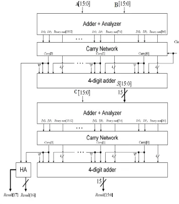
Figure.2 The hardware for performing the addition of three inputs of four digits.
From figure.2 addition of 3-input of 4
delay BCD adder, propagation delay is reduced, but on chip consumed area is increased due to carry network and an analyzer.
So the modification made regarding this approach is area-efficient 3-input
decimal adder presented in [13].There are
in this adder first stage is adder + analyzer it takes three inputs of 4-digits and generate sum using carry look ahead adder(CLA). There are two signal which is DP(Digit Propagate)and DG(Digit Generate). When the sum of three valid BCD numbers is greater then 9 and 19 these conditions are identified by DG
of three BCD numbers is 9,8,18 or 19, these condition are identified by DPi, where, i=0 to 3.
. 1 Conventional hardware architecture for performing the addition of three inputs of four digits.
If the input bits are increased the number of full adder are also increased so the propagation delay is increased. So reduced delay BCD adder is proposed for fast
.2 The hardware for performing the addition of three inputs of four digits.
input of 4-digit reduced propagation delay is reduced, but on chip consumed area is increased due to carry network
modification made regarding this input of 4-digit each, There are three stages in this adder first stage is adder + analyzer it takes three digits and generate sum using carry
look-here are two signal which is DP(Digit Propagate)and DG(Digit Generate). When the id BCD numbers is greater then 9 and 19 these conditions are identified by DGi. When the sum
of three BCD numbers is 9,8,18 or 19, these condition =0 to 3.
Figure.3- The Architecture of 3 for producing DG & DP
In second stage,
sent to carry network which is composed by parallel prefix adder to generate the decimal carry.
Cout[i] = DGi + DPi . Cin[i
And stage 3 is correction stage which added in parallel to the binary sums produced by the stage 1 to produce the real decimal sums Results[15:0].
reduced delay BCD adder, propagation delay is reduced as well as chip consumed area is
Figure.4 the one-digit hardware proposed for 3 CSA+ PG Generator circuit
But this proposed model
number of input digits. i.e. Limited number of digits in input.
Thus, in the next Section our proposed model modified the previous model with reduced delay and high area efficiency through generic
input.
The Architecture of 3-input Adder+Analyzer producing DG & DP
In second stage, DGi and DPi signals are
sent to carry network which is composed by parallel prefix adder to generate the decimal carry.
. Cin[i-1]
And stage 3 is correction stage which added in parallel to the binary sums produced by the stage 1 to produce the real decimal sums Results[15:0]. In this 3-input r, propagation delay is reduced chip consumed area is also reduced .
digit hardware proposed for 3-inputs CSA+ PG Generator circuit
this proposed model is limited for fixed number of input digits. i.e. Limited number of digits in
4-3. PROPOSED GENERIC ARCHITECTURE OF AREA- EFFICIENT DECIMAL ADDER WITH
FOUR INPUTS
The proposed model is consisting of FPGA implementation of generic reduced delay and area efficient 4-input BCD adder. It is the modification Area Efficient 3-input Decimal adders using simplified carry and sum vectors , presented in
generator circuits and the recursive gen
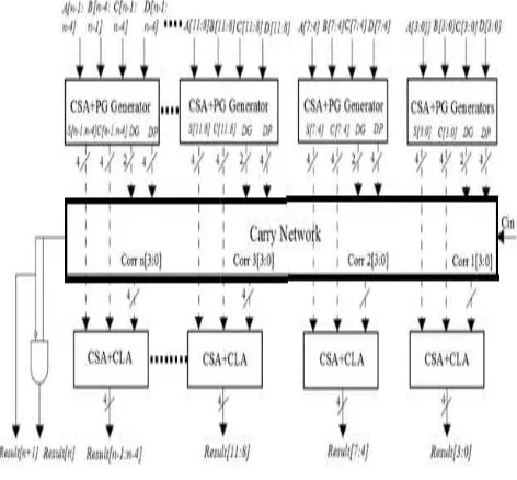
correction terms, this proposed decimal adders could perform efficient summations with 'm' inputs with 'n' number of digits of operands. The proposed BCD adder consists of four stages, each input is divided into n In proposed design has
addition with 4 inputs A,B,C,D with
and sent to the CSA+PG Generator to product the digit sums and carries with digit propagation
signals, then using Carry Network to
decimal carries, in the last stage the sums can be computed by adding the digit sums and
correction values using carry save adders (CSA) plus bit carry look-ahead adders (CLA).
signals for each digit are computed by Carry Network in a parallel-prefix way, the carry propagation for the last stage can be removed.
Figure.5. The one-digit hardware of our proposed CSA+ PG Generator circuit.
As there are four inputs, use of carry save adders to produce sums S[(4*i)+3:4*i] and the carries C[(4*i)+3:4*i] of four inputs first. T
signals to indicate the conditions of sums and the depending upon the carry-outs from the lower digits.
PROPOSED GENERIC ARCHITECTURE OF EFFICIENT DECIMAL ADDER WITH
FOUR INPUTS
proposed model is consisting of FPGA implementation of generic reduced delay and area It is the modification of input Decimal adders using simplified , presented in [].Using proposed rator circuits and the recursive generation of proposed decimal adders could perform efficient summations with 'm' inputs with 'n' proposed BCD adder consists of four stages, each input is divided into n- bits. In proposed design has perform decimal addition with 4 inputs A,B,C,D with each input is n-bits sent to the CSA+PG Generator to product the digit arries with digit propagation and generation signals, then using Carry Network to obtain the real decimal carries, in the last stage the sums can be computed by adding the digit sums and carries with correction values using carry save adders (CSA) plus
Since the correction signals for each digit are computed by Carry Network in prefix way, the carry propagation for the last
digit hardware of our proposed CSA+ nerator circuit. outs from the lower digits.
Table I: The digit generation and propagation signals for identifying the conditions of sums in each digit
The addition of 4-inputs
can reduced the delay and it is more area efficient. Figure.6 The architecture of our proposed N
input decimal Adder
4. SUMULATION RESULTS
The code which has been proposed
efficient decimal adders with four inputs using VHDL programming and synthesized using
having modelsim 5.4a with project navigator Let’s take numerical example
result's snapshots for diffirent n
Example1.
When, No. of bits(n)=16,
Signals Conditions of the sum in each digit
DGi[1] >9
The digit generation and propagation signals for identifying the conditions of sums in each digit
inputs of n-bits architecture can reduced the delay and it is more area efficient.
The architecture of our proposed N- digit four
SUMULATION RESULTS
proposed are generic area-efficient decimal adders with four inputs using VHDL
and synthesized using Xilinx software having modelsim 5.4a with project navigator.
numerical examples and their simulation t's snapshots for diffirent n-bits for each 4-inputs
No. of digits (m) = 4
A=7865
B=3482
C=9634
D=3482
Figure.7.1 Simulation results of Examples-1
Example2.
When, n=24 and m=6
A=347621
B=567438
C=236547
D=686461
Figure.7.2- Simulation results of Examples-2
5. CONCLUSION
The Proposed FPGA implementation of generic area efficient four input i.e., each having m- digits and n-bits, adder using CSA and CLA is coded in VHDL. This adder presents minimum delay compare to previous adder and it acquire less chip area and power consumption is also lesser than other adder by using power prime.
This generic approach for 4-inputs in future can be perform addition for multiple input. In future, this generic approach for 4-input, is further can be perform addition for multiple inputs with reduced delay and high area efficiency.
REFERENCES
[1]. M. S. Schmookler and A.W.Weinberger. ‘‘High Speed Decimal Addition,’’ IEEE Transactions on Computers, Vol. 20, No. 8, pp.862--867, Aug. 1971.
[2].M. A. Erle, M. J. Schulte, and J. M. Linebarger, “Potential speedup using decimal floating-point hardware,” Proc. of the Thirty-Sixth Asilomar
Conference on Signals, Systems and Computers,
Vol. 2, pp.1073–1077, Nov. 2002.
[3]. M. F. Cowlishaw, “Decimal Floating-Point: Algorism for Computers,” Proc. of 16th IEEE
Symposium on Computer Arithmetic (ARITH-16),
pp. 104–111, June 2003.
[4]. R.D. Kenney and M.J. Schulte, ‘‘Multioperand Decimal Addition,’’Proc. IEEE Computer Society Ann. Symp. VLSI, pp. 251-253, Feb.2004.
[5]. R.D. Kenney and M.J. Schulte, ‘‘High-speed multioperand decimaladders,’’ IEEE Transactions on Computers, pp. 953-963, Vol. 54, No.8, Aug. 2005.
[6] A. Bayrakci and A. Akkas, “Reduced delay BCD adder,” Proc. IEEE 18th International Conference
on Application-specific Systems, Architectures and Processors, (ASAP), pp. 266-271, July 2007.
[7]. G. Bioul, M. Vazquez, J. P. Deschamps, and G. Sutter, "Decimal addition in FPGA," Proc. SPL. 5th Southern Conference on Programmable Logic, pp. 101-108, 2009.
[8]. H. Nikmehr, B. Phillips, and C. -C. Lim "Fast Decimal Floating-Point Division," IEEE Transactions on Very Large Scale Integration (VLSI) Systems, Vol. 14, No. 9, pp. 951-961, Sept. 2006.
[9]. T. Lang, and A. Nannarelli, "Division Unit for Binary Integer Decimals," Prof. 20th IEEE International Conference on Application-specific Systems, Architectures and Processors (ASAP),pp. 1 7, 2009.
Architecture," IEEE Transactions on Computers, Vol. 56, No. 6, pp. 727-739, June 2007.
[11]. L. -K. Wang, M. A. Erle, C. Tsen, E. M. Schwarz and M. J. Schulte,"A survey of hardware designs for decimal arithmetic," IBM Journal of Research and Development, Vol. 54, Issue 2, pp. 8:1-8:15, 2010.
[12]. P. Parhami, Computer Arithmetic: Algorithms and Hardware Designs.New York: Oxford Univ. Press, 2000.