Communication at the
Extremes of Computing
Thesis by
Matthew Loh
In Partial Fulfilment of the Requirements
for the Degree of
Doctor of Philosophy
CALIFORNIA INSTITUTE OF TECHNOLOGY
Pasadena, California
2013
©2013
Matthew Loh
Acknowledgements
Although only one person graduates as a direct result of this dissertation, there are a great
many without whose efforts, great and small, its completion would have been impossible.
First among these is my advisor, Prof. Azita Emami-Neyestanak. Being the very first student
to join her group, I have been impressed by her dedication to excellence both as a researcher as
well as a teacher and mentor, and how she has developed as both during my time as her student.
Her support, advice and encouragement have been a defining and essential part of my journey
through graduate school.
I would like to thank the members of my candidacy and defense committees, Prof. Ali
Hajimiri, Prof. Yu-Chong Tai, Prof. Dave Rutledge and Dr. Sander Weinreb, for their willingness
to participate in and evaluate my research, and for their probing questions and valuable input.
The beginning of graduate studies places you at the bottom of a steep and daunting learning
curve; not least among the challenges is figuring out how to build a test-setup for the chips you
have so painstakingly designed. For patiently helping me to learn the ins-and-outs of high-speed
PCB design and wirebonding, and providing much advice on (and loans of) test equipment, I am
deeply indebted to Dr. Sander Weinreb, Hamdi Mani, Steve Smith and Hector Ramirez.
I would also like to express my gratitude to the students and post-doctoral scholars of the
Mixed-Signal Integrated Circuits and Systems (MICS) and Caltech High-speed Integrated
Circuits (CHIC) groups at Caltech; in no particular order, Juhwan Yoo, Meisam Hornarvar
Nazari, Mayank Raj, Manuel Monge, Saman Saaedi, Krishna Settaluri, Kaveh Hosseini, Steve
Bowers, Ed Keehr, Kaushik Sengupta, Florian Bohn, Aydin Babakhani, Hua Wang, Kaushik
Dasgupta, Alex Pai, Behrooz Abiri, Constantine Sideris, Amir Safaripour and Firooz Aflatouni.
The positive atmosphere that exists on the third floor of Moore is sustained by their dedication,
both to research itself as well as to each other as friends and colleagues. Much that I have
accomplished through my time as a graduate student would have been more painful or even
hash out ideas with, and was an unimpeachable apartment-mate for two years.
The smooth operation of the lab, building and department would be impossible without the
efforts of people such as the group administrator, Michelle Chen, the option coordinator, Tanya
Owen, the department administrator, Carol Sosnowski, and the building
engineer/manager/go-to-guy, Kent Potter. Their assistance was essential at all stages of my studies at Caltech, and I owe
them much for their patience and support. I am also indebted for the computer and network
support provided by our IMSS staff, Gary Waters, John Lilley, Chris Birtja and Dan Caballero.
Research in IC design is complex and expensive, enabled in no small part thanks to the
companies and funding agencies that support it; I would like to thank ST Microelectronics and
IBM for chip fabrication, and Intel, the NSF and the C2S2 Focus Center for funding support.
Life at Caltech would not have been complete without the many undergraduates with whom I
crossed paths – whether as a resident of Avery House, teaching assistant for EE 45 or summer
research co-mentor. Though this list is by no means exhaustive, I would like to thank Karthik
Sarma, Chris White, Chris Wong, James Jester, Joseph Schmitz, Ryan Hammerly, Brandon
Hensley, Sam Elder, Dan Thai, Angie Wang, Christina Lee, John Liu, David Lee, Cherrie
Soetjipto, David Hu, Po-Ling Loh, Christian Griset, Nina Ng-Quinn, Brian Peng and Casey
Glick. By offering a refreshing perspective on academics, science and research, and injecting into
my life enthusiasm and verve that is frequently drained away by the demands of graduate study,
their friendship helped sustain and inspire me throughout my time here.
Throughout the course of my graduate studies, I have received a tremendous amount of
support from my parents, Andrew and Li, and my sister, Amanda. I thank them for their love
and prayers, which have been a great encouragement to me despite the distance that separates us.
None of this could have happened but for the grace of God. In the face of setbacks and
triumphs, whether I am enthusiastic or jaded and indifferent, stressed out and frustrated or calm
and relaxed, it is by His providence alone that I am sustained each day.
My wife, Joy, deserves no end of kudos for sticking with me through this whole process,
giving her support and love even when I deserved them least, and for patiently putting up with
my non-committal answers to the age-old question: how long more? I now, finally, have an
Abstract
The scalability of CMOS technology has driven computation into a diverse range of
applications across the power consumption, performance and size spectra. Communication is a
necessary adjunct to computation, and whether this is to push data from node-to-node in a
high-performance computing cluster or from the receiver of wireless link to a neural stimulator in a
biomedical implant, interconnect can take up a significant portion of the overall system power
budget. Although a single interconnect methodology cannot address such a broad range of
systems efficiently, there are a number of key design concepts that enable good interconnect
design in the age of highly-scaled CMOS: an emphasis on highly-digital approaches to solving
‘analog’ problems, hardware sharing between links as well as between different functions (such as
equalization and synchronization) in the same link, and adaptive hardware that changes its
operating parameters to mitigate not only variation in the fabrication of the link, but also link
conditions that change over time. These concepts are demonstrated through the use of two design
examples, at the extremes of the power and performance spectra.
A novel all-digital clock and data recovery technique for high-performance, high density
interconnect has been developed. Two independently adjustable clock phases are generated from a
delay line calibrated to 2 UI. One clock phase is placed in the middle of the eye to recover the
data, while the other is swept across the delay line. The samples produced by the two clocks are
compared to generate eye information, which is used to determine the best phase for data
recovery. The functions of the two clocks are swapped after the data phase is updated; this
ping-pong action allows an infinite delay range without the use of a PLL or DLL. The scheme's
generalized sampling and retiming architecture is used in a sharing technique that saves power
and area in high-density interconnect. The eye information generated is also useful for tuning an
adaptive equalizer, circumventing the need for dedicated adaptation hardware.
On the other side of the performance/power spectra, a capacitive proximity interconnect has
been developed to support 3D integration of biomedical implants. In order to integrate more
functionality while staying within size limits, implant electronics can be embedded onto a foldable
density while decreasing implant size, as well as facilitate a modular approach to implant design,
where pre-fabricated parylene-and-IC modules are assembled together on-demand to make custom
implants. Such an interconnect needs to be able to sense and adapt to changes in alignment. The
proposed array uses a TDC-like structure to realize both communication and alignment sensing
within the same set of plates, increasing communication density and eliminating the need to infer
link quality from a separate alignment block. In order to distinguish the communication plates
from the nearby ground plane, a stimulus is applied to the transmitter plate, which is rectified at
the receiver to bias a delay generation block. This delay is in turn converted into a digital word
Contents
Acknowledgements ... iv
Abstract ... vi
Contents ... viii
List of Figures ... xi
List of Tables ... xvii
Chapter 1: Introduction ... 1
1.1 Interconnect in digital systems ... 2
1.2 High-bandwidth/high-power systems ... 3
1.3 Low-bandwidth/low-power systems ... 4
1.4 Organization ... 6
Chapter 2: High-Speed Electrical Interconnect ... 8
2.1 Clocking ... 9
2.1.1 Sub-rate clocking ... 11
2.2 Clock and data recovery ... 12
2.2.1 Phase detectors for 2x oversampled CDR ... 14
2.2.2 Phase detectors for baud rate CDR ... 17
2.2.3 Clock generation ... 19
2.3 Equalization ... 23
2.3.1 Transmitter pre-emphasis ... 27
2.3.2 Receiver linear equalization ... 28
2.3.3 Decision-feedback equalization ... 29
3.1 Ping-Pong CDR ... 34
3.1.1 Search algorithm ... 37
3.1.2 Search filtering ... 38
3.1.3 System startup and corner cases ... 44
3.2 Shared CDR ... 45
3.3 Implementation ... 46
3.3.1 Phase generator ... 48
3.3.2 Phase generator linearity ... 50
3.3.3 Multiplexers ... 53
3.3.4 Retiming logic ... 55
3.4 Hardware measurements ... 56
3.5 Equalization adaptation ... 64
3.5.1 On-chip links ... 64
3.5.2 Eye-monitor-based adaptive equalization ... 70
3.6 Summary ... 76
Chapter 4: Proximity Communication ... 77
4.1 Capacitive Proximity Interconnect ... 79
4.1.1 Transmitter and receiver design ... 81
4.1.2 Sensing and adapting to misalignment ... 84
4.2 Inductive Proximity Interconnect ... 89
4.2.1 Transmitter and receiver design ... 94
4.3 Proximity Interconnect for Low-power Systems ... 97
5.1 Plate and array design ... 102
5.2 Transceiver array with distributed alignment sensing ... 108
5.2.1 Alignment sensing ... 109
5.2.2 Transmitter and receiver... 117
5.3 Hardware measurements ... 121
5.4 Summary ... 129
Chapter 6: Conclusion ... 131
List of Abbreviations ... 134
List of Figures
Figure 1.1: Chip-to-chip interconnect in a typical 2-socket server. Dashed lines outline
individual CPU chips. Each link shown operates at >1 Gb/s. ... 3
Figure 1.2: Effect of degenerative retinal diseases. ... 5
Figure 2.1: Fundamental clocked link. The transmitter (Tx) sends data ( [ ]) through channel, which the receiver (Rx) converts into an estimate ( [ ]). ... 8
Figure 2.2: Eye diagram, showing sources of noise and timing and voltage margins. ... 9
Figure 2.3: Source-synchronous link with shared timing recovery. ... 10
Figure 2.4: Plesiochronous link. ...11
Figure 2.5: Quarter-rate link. ... 12
Figure 2.6: Generalized 2x oversampled CDR. ... 13
Figure 2.7: Generalized baud rate CDR ... 14
Figure 2.8: Hogge phase detector and timing diagram, showing integrated output gradually rising in response to phase difference between data and clock. ... 15
Figure 2.9: Alexander phase detector, showing sample locations when clock leads or lags. ... 16
Figure 2.10: Example impulse response (adapted from [30]), showing the sample points of converged Mueller-Müller CDR, comparing Type A (red) and Type B (green). Sample points are UI spaced. ... 17
Figure 2.11: Architecture of Mueller-Müller Type A CDR. ... 18
Figure 2.12: Open-loop delay line with 4 delay elements. ... 19
Figure 2.13: Phase interpolator, with weighted buffers ( < 1). Output timing shown in ideal linear case. ... 20
Figure 2.14: (a) PLL block diagram, (b) phase-domain model and (c) typical loop filter. ... 20
Figure 2.15: (a) DLL block diagram and (b) phase domain model. ... 22
Figure 2.16: Pulse response of a legacy 16" server backplane at 12 Gb/s, showing sample points and the effects of dispersion and reflection. ... 24
Figure 2.17: Frequency response of legacy 16" server backplane [37]. ... 24
Figure 2.19: Via (a) before and (b) after back-drilling, showing effect on S21 (of the stub only). ..26
Figure 2.20: Discrete-time (FIR) transmitter pre-emphasis with pre-cursor taps and post-cursor taps. ...28
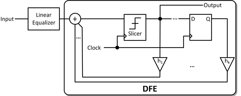
Figure 2.21: Receiver with linear equalizer and DFE. ...29
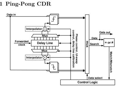
Figure 3.1: Single-pin ping-pong CDR architecture overview. ... 34
Figure 3.2: Ping-pong CDR algorithm. ... 35
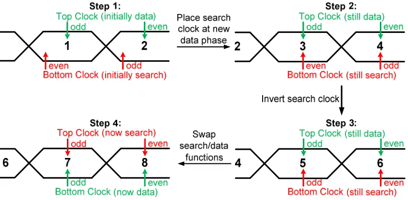
Figure 3.3: Steps in a UI swap process. Even (rising) and odd (falling) edges of the clocks marked. ... 36
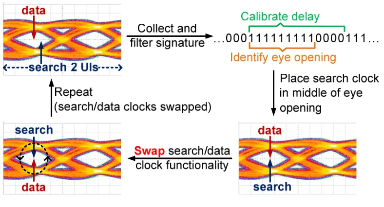
Figure 3.4: Search procedure, showing movement of search clock and numbered eye edges. ... 37
Figure 3.5: CDR operation with eye drifting until UI swap is required. Relevant eye edges are marked and numbered... 38
Figure 3.6: Eye information collection via mismatch counter and AND/OR filter. ... 39
Figure 3.7: Typical BER bathtub, and the probability of mismatch declaration at each phase position with ( = 32) and without ( = 32) repeated averaging. ...41
Figure 3.8: Probability of match-to-mismatch transition detection, = = 32. ...42
Figure 3.9: Peak probability in distribution of match/mismatch transition detection, with and without repeated averaging. ... 43
Figure 3.10: Probability of match-to-mismatch transition detection, = = 128. ... 43
Figure 3.11: AND/OR filter with = 4. ...44
Figure 3.12: Sharing concept and modified draft algorithm, for 3 data pins and 4 clocks ...45
Figure 3.13: Three-pin shared CDR architecture. ...47
Figure 3.14: Phase generator architecture. ...48
Figure 3.15: Delay line with (a) delay cell and (b) phase interpolator. Weak cross-coupled inverters are marked with a ‘W’. ...48
Figure 3.16: Delay line with negative INL and phase interpolator with (a) negative INL, (b) positive INL and (c) ‘crossing’ INL. ...52
Figure 3.17: Search/data multiplexer (only clock routing shown; sample routing is similar). ... 53
Figure 3.18: Retiming logic. ...55
Figure 3.21: Phase generator non-linearity. ... 58
Figure 3.22: Delay line output non-linearity (note that the 0th output is missing, since this is inaccessible due to the configuration of the phase interpolator). ... 58
Figure 3.23: Interpolator INL, across different groups of 8 phase positions (each corresponding to one sweep through the interpolator). ... 59
Figure 3.24: Interpolator DNL, across different groups of 8 phase positions (each corresponding to one sweep through the interpolator). ... 59
Figure 3.25: SJ tolerance with control logic clock at 40 MHz, for 3 x 9 Gb/s PRBS-7 input and BER < 10-12. ... 60
Figure 3.26: (a) Frequency offset tolerance scaling for 3 x 9 Gb/s PRBS-7 input (measured BER < 10-12 and simulated BER < 10-6), with (b) low frequency detail. ... 61
Figure 3.27: Effect of nbase on frequency offset tolerance, simulated on a single channel at 625
MHz with PRBS-7 input and BER < 10-6. ... 61
Figure 3.28: Power breakdown and scaling performance ... 62
Figure 3.29: On-chip links, within the context of a two-socket server. Individual CPU chips indicated by dashed lines. (a) repeated, full-swing and (b) RC-limited, low-swing links shown. ... 64
Figure 3.30: Bandwidth density (Hz/um) estimated over wire pitches up to 3 um in metal 7 of a typical 9-metal 65 nm process ... 67
Figure 3.31: Bandwidth density-optimized on-chip channel in typical 9-metal 65 nm process, with frequency response for 10 mm length... 68
Figure 3.32: Pulse response of channel in Figure 3.31, at 5 Gb/s. ... 68
Figure 3.33: (a) Classic DFE with discrete-time FIR feedback, and (b) DFE with continuous-time RC feedback, replacing all N taps in the FIR feedback. ... 69
Figure 3.34: Simulation of ping-pong CDR-based adaptive equalizer, showing stages of
operation. ... 74
Figure 3.35: Histograms of received signal level at sample point, comparing continuous-time IIR DFE with ping-pong CDR-based adaptation @ 5 Gb/s (red) against 7-tap FIR DFE with SS-LMS adaptation @ 3.25 Gb/s (green) ... 75
Figure 4.2: Capacitive link, showing transmit driver resistance and receiver bias resistance ...81
Figure 4.3: Variable-threshold comparator used as a receiver in a capacitive proximity interconnect, with waveforms showing principle of operation ...82
Figure 4.4: Example precharge-and-evaluate input stage (adapted from [75]). During precharge (clock is high), bias point is set by shorting the input and output of the input inverter stage, causing it to enter its metastable state. The D flip-flop evaluates the current bit at the rising edge of the clock ... 83
Figure 4.5: High Rbias achieved using leakage device ... 83
Figure 4.6: Chip-to-chip alignment can be described in terms of 6 axes: 3 linear (x, y and z) and 3 angular (θx, θy, θz) ...84
Figure 4.7: Vernier bar-based alignment sensor [9]. Output of flip-flop depends on the most strongly coupled transmitter bar, and can be unknown (‘X’) if two adjacent transmitter bars are equally-well coupled ...85
Figure 4.8: Multi-plate alignment sensor with passive target chip [79], for (a) in-plane (x- and y-axis) alignment and (b) vertical (z-axis) alignment, showing equivalent circuits...86
Figure 4.9: Ring oscillator-based alignment sensor [80] ...87
Figure 4.10: Adaptation of transmitter array to receiver array alignment [81] ...88
Figure 4.11: Circular wire loops for calculation of mutual inductance ...89
Figure 4.12: Comparison of mutual inductance between two single-loop wires with r1 = r2 = 50 µm and capacitance between two 50x50 µm square parallel plates in silicon dioxide (εr = 3.9), over different amounts of separation ...90
Figure 4.13: Coupling co-efficient between two single-loop wires with r1 = r2 = 50 µm, over different amounts of separation ...91
Figure 4.14: Ideal inductively-coupled link, with equivalent circuit ...91
Figure 4.15: Inductively-coupled link with parasitics. ...92
Figure 4.16: Simplified inductively-coupled link model, using a unilateral coupled inductor ...92
Figure 4.17: Magnitude response of circuit with full parasitic model, compared with simplified circuit using unilateralized coupled inductor model, with L1 = L2 = 5 nH, k = 0.2, Rp1 = Rp2 = 100 Ω, Rtx = 10 kΩ, Cp1 = 75 fF and Cp2 =100 fF...94
operation waveforms ... 95
Figure 4.20: Pulsed-current transmitters: (a) H-bridge with delay line, (b) single-ended with storage capacitor and (c) operation waveforms, showing small timing margin available at receiver ... 96
Figure 4.21: Survey of wearable and implantable biomedical devices reported in ISSCC
between 2010 and 2013 ... 98
Figure 5.1: Top-down view of the sensor array, in (a) best-case (maximum overlap) and (b) worst-case (minimum overlap) alignment. Active sensor plates are shaded in
green, and the associated target plate is outlined ... 103
Figure 5.2: Plate and switch configurations for (a) = 2, (b) = 3 and (c) = 4. The highlighted group of active sensor plates indicates the worst-case loading condition, where the largest number of inactive switches are connected to the active plates ... 104
Figure 5.3: Link gain for different values of , when plates are in best-case alignment ... 106
Figure 5.4: Link gain for different values of , when plates are in worst-case alignment ... 106
Figure 5.5: Dielectric and metal layers used to form plate structure, and sensor/target array arrangement (target chip outline not shown for clarity) ... 107
Figure 5.6: Architecture of the sensor and target cells, with key functional blocks indicated ... 108
Figure 5.7: (a) Standard TDC using a single delay line compared to (b) a vernier TDC. Flip-flops act as arbiters, indicating which edge arrives earlier ... 110
Figure 5.8: Sensor array structure, showing TDC path for alignment sensing at indicated
plates ... 110
Figure 5.9: Rectifier and associated timing diagram ... 111
Figure 5.10: (a) Differential voltage-controlled delay line with variable-threshold output buffer and (b) variable-delay inverter used in VCDL unit cell ... 112
Figure 5.11: TDC delay cell and arbiter ... 113
Figure 5.12: Target-to-sensor link gain vs. air gap, using = 2, target plate size of 60x60 µm and no parylene ... 114
Figure 5.14: Two adjacent groups of sensor plates used for x-axis alignment sensing. 0 ≤ ≤ 1; when = 0, target plate is all the way to the left (completely over 1).
Likewise, when = 1, target plate is completely over 2 ... 115
Figure 5.15: In-plane alignment estimation, using simulation results with various dielectrics between the two chips ... 116
Figure 5.16: Equivalent circuit of the capacitive link, with switch parasitics ( and ) introduced. is assumed to be very large, and is omitted ... 117
Figure 5.17: Tri-state buffer-based transmitter, with leakage path to define plate bias voltage .. 118
Figure 5.18: Source-follower buffer with gateable Wilson current mirror bias ... 118
Figure 5.19: 3-stage hybrid low-pass filter ... 119
Figure 5.20: Input slicer and offset compensation (SR latch not shown). ‘Reset’ zeroes the offset compensation capacitor and ‘oc_en’ is asserted during offset compensation calibration ... 120
Figure 5.21: Input slicer offset estimated across 200 Monte Carlo simulation runs, (a) before and (b) after offset compensation ... 121
Figure 5.22: Die micrograph, with sensor and target arrays marked ... 121
Figure 5.23: Sensor and target cell layout detail ... 122
Figure 5.24: Test setup. Inset: Detail of chips when brought into alignment ... 123
Figure 5.25: Effect of offset compensation on a single sensor cell's VCDL/TDC-based ADC ... 124
Figure 5.26: The effect of VCDL/TDC offset compensation on (a) offset error and (b) total error, measured over 144 sensor cells across 6 chips ... 125
Figure 5.27: Alignment sensor output under vertical (z-axis) separation ... 125
Figure 5.28: Comparison of measured and simulated (quantized and unquantized) in-plane (x- and y-axis) alignment sensing, with (a) air-only and (b) 2x6 µm parylene dielectrics ... 126
Figure 5.29: Alignment sensor output under in-plane (x- and y-axis) misalignment, for 4, 5, 6, 2x4 and 2x5 µm parylene dielectrics ... 127
Figure 5.30: Achieved in-plane alignment sensor resolution vs. parylene dielectric thickness ... 127
List of Tables
Table 1.1: Approximate chip-to-chip I/O bandwidths, total system power, link distance and form-factor for different system types. ... 2
Table 2.1: Truth table for Alexander phase detector. ‘X’ states indicate don’t cares, since X≠Y cannot normally co-exist with X=Z. ... 16
Table 3.1: Performance summary, 3 x 9 Gb/s ping-pong CDR ... 63
Table 5.1: Number of inactive switches loading the active group of plates, for various values of ... 105
Table 5.2: Performance summary, 12 x 60 Mbps capacitive proximity interconnect with
Chapter 1:
Introduction
In observing that the economically-efficient number of components per integrated circuit (IC) had
increased 2x every year between 1962 and 1965 and predicting that this trend could be sustained,
Moore’s seminal 1965 paper [1] provided an impetus and objective for what is, perhaps, the greatest economic engine in history. Certainly it has sparked a revolution in computation and
communication whose full effects are only beginning to be understood.
Integration of more and smaller transistors has allowed increasing complexity in the design of
processing and communication units, while driving (at least initially) a rise in clock speeds and
power efficiency. Even a slowdown in voltage scaling and the advent of power consumption as a
major limiter in clock speed scaling have not prevented continued advances in computational
power; increases in transistor density have enabled designers to work around these limits by
adopting new approaches such as multi-core and heterogeneous computing. A good example of
this is the incorporation of vector processors, such as graphical processing units (GPUs), into a
general-purpose computational architecture.
The economics of CMOS scaling have also pushed ICs into new and unusual spaces. For
example, the availability of very cheap, highly-integrated microcontrollers has spurred a
renaissance in hobbyist electronics and led to innovation in ubiquitous computing – the idea that electronics can be made cheap and small enough to afford a measure of ‘intelligence’ and interactivity to even the most mundane of objects. In practice, this has enabled a range of
projects from wearable electronics [2] to sophisticated, home-built 3D printers [3]. The versatility
of CMOS has also made it an attractive platform for implementing sensing, stimulus, processing
and communication systems in biomedical implants. The high level of integration possible makes
it particularly attractive in this space, where power consumption and package size are of primary
1.1
Interconnect in digital systems
The power of scaling, then, has created a strong economic incentive to apply CMOS technology in
a diverse range of applications across the power consumption, performance and size spectra. Of
course, where there is computation, a need exists to communicate with and between the elements
realizing that computation. Whether this is to facilitate pushing data from node-to-node in a
high-performance computing (HPC) cluster, between CPU and memory in a desktop, or from the
receiver of wireless link to a neural stimulator in a biomedical implant, interconnect can take up a
significant portion of the overall system power budget (e.g. ~11% for off-chip interconnect in the
Intel Nehalem-EX microprocessor [4]). As a result, considerable design effort is expended to
ensure that interconnect blocks operate as efficiently as possible, while still meeting performance
and robustness targets.
Server/workstation >2000 >300 >10 cm >60
Desktop 200-300 60-100 5-30 cm 20-40
Laptop 190-270 20-35 5-20 cm 1-4
Tablet 100 10 5-10 cm 0.25-0.5
Smartphone 40 <1 1-10 cm 0.07-0.12
Biomedical implant <0.1 <0.1 <1 cm <0.01
Table 1.1: Approximate chip-to-chip I/O bandwidths, total system power, link distance and form-factor for different system types.
Table 1.1 gives a sense of the scale of the design problem at the time of writing; depending on
the target application, chip-to-chip I/O bandwidths range over 4 orders of magnitude, and system
power consumption and form-factor over 3 orders of magnitude or more. Since a single
interconnect methodology cannot address such a broad range of requirements efficiently,
chip-to-chip communication systems are typically customized to specific applications. Nevertheless, there
are a number of design concepts that typify efficient interconnect design, no matter what the
1.2
High-bandwidth/high-power systems
High-performance multi-processor/multi-socket systems, typically used in the server and HPC
space, require many high-speed communication links (Figure 1.1). Whether these are between
processors, to system memory or to high-performance add-in modules (such as GPUs), the
fundamental challenge is the same: realizing multi-Gb/s links within strict power budgets, in the
presence of strong attenuation and crosstalk in the channel.
Figure 1.1: Chip-to-chip interconnect in a typical 2-socket server. Dashed lines outline individual CPU chips. Each link shown operates at >1 Gb/s.
Historical trends are not promising – a survey conducted in 2009 showed that, while link
power efficiency has improved at a rate of about 20% per year, the demand for bandwidth has
outstripped this improvement, increasing between 2 to 3x annually [5]. The same survey
suggested that, in order to meet the requirement for multi-Tb/s operation, link energy efficiencies
would have to improve an order of magnitude, from 10 pJ/b to 1 pJ/b. To achieve such a target
fast enough to meet demand, business-as-usual improvements, which typically rely on the effects
of CMOS scaling, are inadequate. Indeed, because chip-to-chip communication is fundamentally a
mixed-signal problem (converting a noisy analog waveform into a reliable digital bit-stream)
traditional approaches to solving it have relied heavily on analog techniques. As CMOS
technology scaling is driven largely by the demand for more and faster digital switches, it is
precisely the analog blocks that suffer most from the transition to finer-geometry processes.
design, with an emphasis on more digital-like solutions. Concurrently, it is important to pursue
higher-level optimizations such as sharing hardware, not only between links, but also between
functions such as synchronization and equalization.
1.3
Low-bandwidth/low-power systems
If there is an incentive to pursue unconventional approaches to link design in order to address the
challenges faced in high-performance systems, this is even more acutely felt as ICs start to
address non-traditional, power- and form-factor-sensitive arenas such as ubiquitous computing
and biomedical devices.
Although they address very different problems, the intent of both biomedical and ubiquitous
computing devices is frequently the same: sense the environment, perform some simple
computation to understand the resulting data and respond appropriately. A typical system, then,
will include one or more sensors, a processor of some sort (frequently optimized for low power,
small size and low cost), a set of actuators and a wireless interface. A battery might also be
necessary if power is not delivered wirelessly or scavenged from the environment.
Many of these applications are specialized and low-volume. Producing unique systems-on-chip
(SoCs) for each of them is prohibitively expensive, and existing printed circuit board (PCB)
fabrication techniques simply cannot achieve the compactness required. Proximity communication
[6] provides a means to overcome these limitations – inductive coils (e.g. [7], [8]) or capacitive
plates (e.g. [9], [10]) can be fabricated in the top-level metal of a standard CMOS process, with
no extra fabrication steps. When these coils or plates are placed in close proximity with each
other, inductive or capacitive coupling forms an electrical link that can transfer data and/or
power. Since it uses the existing metal stack, proximity communication involves minimal extra
cost and enables manufacturing techniques such as Brick-and-Mortar [11], which envisions the
mass production of a library of IC sub-blocks (‘bricks’) that can be placed on a standardised
communications substrate (‘mortar’). By customizing the mix of bricks used, specialized systems
can be built up for particular applications in cost-effective fashion, while still retaining a large
To make this discussion more concrete, consider a retinal prosthesis for treating diseases such
as retinitis pigmentosa (RP, a degenerative eye disease that gradually reduces a person’s field of
vision. Eventually, they can become effectively blind) and age-related macular degeneration
(AMD, where the macula, or central portion of the retina, is damaged, resulting in loss of visual
fidelity. Again, this can result in clinical blindness) [12].
Figure 1.2: Effect of degenerative retinal diseases.1
Very few options exist for treating late-stage RP or AMD. In both diseases, although the
photoreceptors in the retina have ceased to function properly, the nerves in the retina are still
healthy. Therefore, retinal prostheses can be used to electrically stimulate the still-functioning
nerves with visual data, restoring partial vision. Although early devices have been successfully
implanted, they have suffered limitations in the amount of stimulation current able to be
delivered [13] or the number of electrodes (just 16 in [14]). Since visual fidelity is closely related
to the number of electrodes that successfully stimulate the retinal neurons, scaling these systems
to thousands of electrodes is an important (and challenging) task. However, high voltages (~5-10
V) are necessary to drive the desired stimulus currents, preventing the use of finer-geometry
CMOS technologies, which have insufficiently large breakdown voltages. As a result, die size (e.g.
8x8 mm2 for a proposed 1024-electrode array [15]) prevents a straightforward increase in the number of electrodes, since the prosthesis is intended for implantation in the eye and the incision
size is limited.
In order to work around this size limit, large multi-electrode systems can be split into
multiple chips and placed on a flexible, bio-compatible substrate, such as Parylene-C [16], which
1 From National Institutes of Health, National Eye Institute. Available:
can be folded compactly for implantation. By engineering the folding (‘origami’) of the parylene,
it can be made to assume useful shapes once deployed (e.g. an inductive coil for power/data
delivery [17]). A longer-term objective would be to build up a library of standard and useful ICs
(e.g. neural stimulator driver, wireless data/power management, low-power processor) which are
compatible with parylene integration, so application-specific implants can be put together from
pre-fabricated, mass-produced modules in a manner similar to that proposed by the
Brick-and-Mortar scheme mentioned above.
Indeed, the analogy to Brick-and-Mortar is an apt one, since similar chip-to-chip
communication techniques are appealing when building a modular origami parylene system. Many
ICs in an origami implant will be placed face-to-face with each other when it is deployed,
facilitating the use of proximity communication. The ability to communicate wirelessly helps to
reduce wired communication density, making it easier to develop more compact implants.
Additionally, wireless module-to-module communication eases the assembly of custom implants
from origami-based library blocks. As a result, proximity communication (whether via capacitive
or inductive coupling) is a promising avenue of research for chip-to-chip interconnect in
low-power systems such as this.
1.4
Organization
This dissertation is composed of two major parts, corresponding to the two extremes of digital
system interconnect described in the introduction. The first addresses high-speed electrical
interconnect: Chapter 2 provides an overview of the terminology and design techniques used in
this domain, including techniques for synchronization and clock recovery as well as equalization.
Chapter 3 builds on this background and presents a novel all-digital ‘ping-pong’ clock and data
recovery system, which is extended for use in an adaptive equalizer. The second half of this
dissertation addresses electrical interconnect in the context of low-power, space-constrained
systems by using the example of proximity interconnect for origami implants. Chapter 4 describes
the development of capacitively and inductively-coupled wireless communication from the very
approaches for chip-to-chip and chip-to-package high-speed interconnect. Design considerations
for proximity communication in low-power systems is discussed, and Chapter 5 details an
implementation of just such a system for use in origami implants. Throughout, it is sought to
demonstrate the importance of a more-digital, adaptive, shared and multi-functional hardware
Chapter 2:
High-Speed Electrical
Interconnect
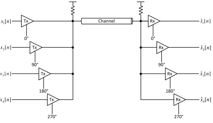
Channel
Tx
Rx
] [n
x xˆ[n]
Tx Clock
Rx Clock
Termination
Termination
Figure 2.1: Fundamental clocked link. The transmitter (Tx) sends data ( [ ]) through channel, which the receiver (Rx) converts into an estimate ( [ ]).
Figure 2.1 shows the components and configuration of the most basic clocked electrical link: a
transmitter, receiver and channel, with clocks and termination resistors at each end to time the
data and reduce the effect of reflections due to impedance discontinuities. Since the signal sent
down the channel exists in the continuous time, analog domain, the purpose of the receiver is to
determine the optimum decision point, in time and amplitude, to estimate the original bit-stream
and minimize errors. In an additive white Gaussian noise (AWGN) channel, the bit error rate
(BER) is classically characterized by the voltage margin, , at the sampling point [18]:
= exp #$% ' (& )
2 *
where & is the root-mean square (RMS) voltage noise; since Gaussian noise is assumed, this is
equivalent to the noise standard deviation. Besides voltage noise, the second major contributor to
BER is timing uncertainty at the receiver. Like voltage noise, this uncertainty is a random
process, and it is characterised by the jitter of the receiver clock as well as that of the transmitted
of reducing the voltage margin and degrading the BER. This effect is of particular concern as
data rates increase, since jitter can become a substantial portion of a data period (also known as
a unit interval, UI). As a result, timing margin can become a larger concern than voltage margin
in high-speed links [19]. A helpful and common tool for visualizing the effects of noise and jitter
on a link is the eye diagram, which is generated by superimposing many UIs of the data signal on
top (Figure 2.2).
Figure 2.2: Eye diagram, showing sources of noise and timing and voltage margins.
The simple link structure described in Figure 2.1 forms the foundation for virtually all
chip-to-chip communication in modern computing systems; indeed, for lower data rates, it can be used
essentially unmodified. At higher (>1 Gb/s) data rates, however, a number of issues make this
simple structure untenable, and designers have adopted a set of enhancements to deal with them.
2.1
Clocking
One of the challenges that arise at higher data rates is timing and synchronization. As the UI
size, or bit time, decreases, the receiver has smaller and smaller timing margin and clocking
naturally becomes more difficult. In order to provide a framework for discussion on this subject, it
- Synchronous: from the Greek root meaning ‘same’. In a synchronous link, the transmitter and receiver clocks are assumed to have the same frequency and phase. This
is generally only a tenable assumption at low data rates.
- Mesochronous: from the Greek root meaning ‘between’. In a mesochronous link, the transmitter and receiver clocks are assumed to have the same frequency, but may be
out-of-phase. A popular sub-set of this category is the source-synchronous link, where the clock is generated at the transmitter and forwarded along with the data.
- Plesiochronous: from the Greek root meaning ‘near’ or ‘similar’. In a plesiochronous link, the transmitter and receiver clocks may have slight differences in frequency. The
receiver is required to align its clock by extracting timing information from the incoming
data stream.
- Asynchronous: an asynchronous link is not really clocked at all. Rather, it uses either control symbols inserted in the data stream itself or handshaking signals to convey timing
information.
As the mesochronous/source-synchronous and plesiochronous styles are most frequently
adopted for high-speed interconnect design, they shall be the focus of the discussion here.
Since they require relatively straightforward timing recovery at the receiver (when compared
to plesiochronous links), source-synchronous links are frequently used in computer systems,
particularly where the link is composed of many data pins and the relative cost of adding a clock
pin is small. Examples of source-synchronous links include memory interfaces such as DDR3 [20],
and chip-to-chip interfaces such as HyperTransport [21] and QuickPath [22]. A typical block
diagram is shown in Figure 2.3. With the clock forwarded along with the data, it will (ideally)
experience similar amounts of skew and jitter, simplifying the task of synchronization at the
receiver [23]; frequently, a single timing recovery block can be used across a bundle of many data
pins that have the same origin. This assumption becomes untenable at higher data rates,
however, where fabrication tolerances (e.g. of trace length) result in phase variation between data
pins that is significant relative to a UI.
Timing
forwarded clock, but complicates synchronization at the receiver by requiring it to extract timing
information from the incoming data stream, and synchronize a local clock to it (Figure 2.4). The
lower routing overhead makes plesiochronous links popular for communication between add-in
cards and over server backplanes (e.g. PCI-Express [24]), which generally have to travel cover
longer distances than the source-synchronous links described previously.
2.1.1
Sub-rate clocking
In a classical ‘full-rate’ link, the period of the clock is the same as the length of a UI and, for
example, a 5 Gb/s link will operate with a 5 GHz clock. At multi-Gb/s data rates, however, the
the process of timing recovery. As a result, designers use sub-rate clocking schemes. These are
essentially multiplexing/demultiplexing schemes, where the clock operates at some integer
fraction of the data rate and the data is transmitted and/or received using multiple phases of a
clock period (Figure 2.5). Although it is, in principle, possible to generate as many phases of the
clock as desired and lower the clock rate arbitrarily, practical concerns typically limit link
implementations to half- and quarter-rates; in a half-rate link, the positive (0°) and negative
(180°) edges of the clock can be used directly, and it is fairly straightforward to generate in-phase
(0°) and quadrature (90°) clocks and their negations (180° and 270°) for quarter-rate systems.
Half-rate systems are particularly popular (commercial examples include the DDR SDRAM,
HyperTransport and QuickPath interfaces mentioned earlier), since clock generation is typically
done differentially and the negated clock is essentially free. Another benefit of half-rate systems is
that they match the bandwidth requirements of clock and data, which is particularly useful in
source-synchronous links where clock and data are transmitted over similar channels.
Channel
As seen in the previous section, timing recovery is an important part of a high-speed link. In a
assumed to be the same, and the task of the timing or clock and data recovery (CDR) is to
estimate and align their phases. This task gets considerably more challenging in a plesiochronous
link, where the CDR must also compensate for frequency differences between clock and data.
Classical CDR techniques2 can be split into two broad classifications: 2x oversampled and baud rate. A generalized 2x oversampled CDR is shown in Figure 2.6. The first phase of the clock
is sent to the data slicer, and is placed near the middle of the eye. On its own, the data slicer
provides no useable information about phase. Therefore, a second clock is used to slice the
incoming signal at some phase offset from the data clock. The phase detector makes a comparison
between the outputs of both slicers to determine the phase of the incoming data, and this
information can in turn be filtered to generate a control signal for the clock generator that
produces the two clock phases. This technique is appealing because the phase detector used takes
inputs that have already be sliced into digital values, and is therefore relatively straightforward
to implement in highly-scaled process technologies. Additionally, its operation is largely
pattern-independent; system bandwidth is determined only by transition density, rather than the presence
of particular bit patterns. The primary disadvantage is the requirement for the generation and
distribution of two clock phases, which can increase the power consumption of such a CDR.
Figure 2.6: Generalized 2x oversampled CDR.
A baud rate CDR (as the name suggests) uses sampler(s)3 operating on only a single phase of the clock, operating at the symbol, or baud, rate (Figure 2.7). Phase information is extracted by
comparing characteristics (such as the voltage) of the present sampler output with those obtained
previously. Requiring only a single clock phase gives the baud-rate approach a clear advantage
over 2x oversampled CDRs; however, the analog processing required makes integration of such
CDRs difficult4. Techniques to overcome this limitation are described below.
Figure 2.7: Generalized baud rate CDR
2.2.1
Phase detectors for 2x oversampled CDR
One classic example of a phase detector for use in a 2x oversampled CDR is the Hogge, or linear,
phase detector, first described in 1985 [25]. The Hogge phase detector (Figure 2.8) operates by
detecting transitions in the incoming data and generating pulses whose width is proportional to
the phase difference between clock and data. Since the average of this output (Y in Figure 2.8) is
dependent on the data transition density, a reference half-clock pulse (Z) is generated at every
data transition and subtracted from this phase difference. The result can be integrated and used
3 A note about terminology: a ‘sampler’ converts a continuous-time input into a discrete-time
output, but does not make any decision about what bit this output represents (hence it is still analog, or continuous-value). Conversely, a ‘slicer’ combines the functions of sampler and decision element, and converts a continuous-time input into a digital value that is both discrete-time and discrete-value. Therefore, a 2x oversampled CDR uses slicers, since it operates on digitized values, while a classical baud rate CDR uses samplers, since it requires analog values.
4 An exception to this is links which use ADC-based receivers. Though a full discussion of this
to control a clock generator, which will lock half a UI away from the edge of the eye, as long as
the clock duty cycle is 50%. Note that this sampling point is optimal so long as the eye is
symmetric, which is not always the case.
The Hogge phase detector has a number of drawbacks that limit its utility in high-speed
digital systems. For instance, its output pulse width is proportional to the residual phase error, so
good resolution requires narrow pulses. Since these pulses must naturally be a small fraction of a
UI, producing them requires fast, power-hungry XOR gates. This resolution limit is compounded
by the static phase offset due to the non-zero (and likely mismatched) clock-to-Q delays of the
flip-flops. Hogge’s discrete implementation corrected for this offset by introducing adjustable
delay lines, but process, voltage and temperature (PVT) variations make this approach
unsuitable for integrated designs. Finally, the linear output of the Hogge phase detector requires
analog processing to control the clock generator, and such processing incurs excessive power and
area penalties in deep sub-micron digital systems. As a result, most recent CDR implementations
(e.g. [26], [27]), are based on an older phase detector first proposed by Alexander in 1975 [28],
which avoids these limitations and generates non-linear output that can be sent directly to a
charge pump or digital loop filter.
Figure 2.9: Alexander phase detector, showing sample locations when clock leads or lags.
X Y Z up dn
0 0 0 0 0
0 0 1 0 1
0 1 0 X X
0 1 1 1 0
1 0 0 1 0
1 0 1 X X
1 1 0 0 1
1 1 1 0 0
Table 2.1: Truth table for Alexander phase detector. ‘X’ states indicate don’t cares, since X≠Y cannot normally co-exist with X=Z.
The Alexander phase detector (Figure 2.9) operates by comparing samples taken on both
edges of the clock. The basic principle of operation is to look for transitions in the incoming data
(X≠Z), then to check if X=Y, which indicates if the clock is leading or lagging the data. Based on
this information, it generates ‘Up’ or ‘Down’ pulses to move the phase of the clock, an action
known as ‘bang-bang’. Table 2.1 shows the truth table for this operation. The two don’t care
states allow a degree of logic simplification; alternatively, they can be used to detect failure states
[29]. Due to its non-linear nature (its output only has three states), a CDR based on an
higher output jitter than a comparable Hogge-based system. The size of the limit cycle is related
to the gain and delay through the CDR feedback loop; larger gain and longer delays produce
larger limit cycles and more jitter. Note that, as in the Hogge phase detector, the Alexander
phase detector is sensitive to clock duty cycle and makes the assumption that the eye is
symmetric, placing the clock half a UI away from the eye edge.
2.2.2
Phase detectors for baud rate CDR
Figure 2.10: Example impulse response (adapted from [30]), showing the sample points of converged Mueller-Müller CDR, comparing Type A (red) and Type B (green). Sample points are
UI spaced.
The prototypical baud rate CDR was proposed by Mueller and Müller in 1976 [30]. It uses
samples of the incoming data to estimate the impulse response of the channel, adjusting the data
clock such that the impulse response of the preceding and succeeding sample points (Figure 2.10)
have certain behaviour. The original paper proposed two variations, Type A, which forces ℎ,-=
ℎ-, and Type B, which forces ℎ-= 0. Comparing the two types in the presence of phase distortion, the authors noted that the Type A system worked best when the impulse response was
close to symmetric, while the Type B system was more tolerant of asymmetries in the impulse
response. However, the Type B estimation function is much more complex and does not lend
itself well to implementation. As a result, the focus of current design has been on variations of
ℎ-$ ℎ,-= . .,-$ .,- .
and adjusting the clock phase such that it is minimized. A typical architecture is shown in Figure
2.11, where . is the voltage value of the kth sample, and . is the digitized value of the kth sample (+1 or -1 for binary data). The output of the phase detector is sent to the loop filter of a
clock generation loop, which performs the low-pass filtering necessary to determine the expected
value.
Figure 2.11: Architecture of Mueller-Müller Type A CDR.
Due to the requirement to delay and process the analog . values, implementations of the
unmodified Type A system are impractical in highly-scaled CMOS. Realizations of this form of
CDR instead rely on a sign-sign reduction of it [31], [32]. Extra slicers with positive and negative
threshold offsets from the nominal decision point are used to produce error signals (/.; /.= 01
when the input exceeds the boundaries defined by the thresholds, and /.= $1 when it is within
the thresholds) that approximate the . values, so (2.2) becomes:
ℎ-$ ℎ,-= /. .,-$ /.,- .
Note that the extra samplers do not constitute a substantial hardware overhead, since their
2.2.3
Clock generation
Figure 2.12: Open-loop delay line with 4 delay elements.
To complete the CDR feedback loop, the output of the phase detector has to be used to control
some form of clock generator. Depending on the clocking scheme used, the generator can range
from the very simple (open-loop delay line for source-synchronous/mesochronous links) to the
complex (phase-locked or delay-locked loop for plesiochronous links with large frequency offsets).
The most basic clock generator for timing recovery is an open-loop delay line with
variable-phase output (Figure 2.12). It is simply a series of delay elements that takes a reference clock as
its input, with a multiplexer to select the appropriate delay element’s output to feed to the
samplers. The multiplexer can be controlled by the up/dn signals from a bang-bang phase
detector. Note that this is not really a clock generator at all, but is more accurately described as
a programmable phase shifter. Due to its open-loop nature, it places no guarantee on the exact
amount of delay that it realizes; as a consequence, it can only correct for phase offsets as large as
the length of the delay line. Any frequency offset between clock and data (as in a plesiochronous
link) will eventually cause the delay line to run out of range and the CDR to break. Even in
mesochronous links this approach faces some challenges. For example, it needs to be at least as
long as the largest expected jitter transient, and the longer the delay line is, the more noise it
accumulates and power it consumes. The resolution of the delay line is also limited to the fastest
realizable delay element; optimistically, this is an inverter with fan-out of 1 (note that the load
imposed by the output multiplexer and wiring ensures that this is, in fact, unachievable). Since
the size of a bang-bang CDR’s limit cycle is at least as large as its clock generator’s smallest step
Figure 2.13: Phase interpolator, with weighted buffers ( <1). Output timing shown in ideal linear case.
The resolution of a delay line can be enhanced through the use of a phase interpolator (Figure
2.13), which takes two adjacent delay line outputs and produces a weighted average of their
phases. In principle, there is no limit to the resolution that can be achieved using such a
technique, but practical considerations (matching, jitter, power, and area) impose an effective
upper bound on the resolution [34].
Increasing the resolution of the open-loop delay line through the use of a phase interpolator
does not, of course, prevent it from running out of delay range. The solution to this problem
instead requires a closed-loop approach, using a phase-locked loop (PLL) or delay-locked loop
(DLL).
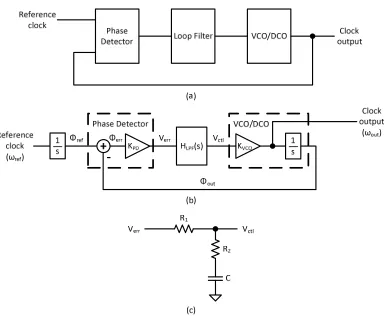
As its name suggests, the PLL works by synchronizing the phase of its internal oscillator to
an external reference. In order to accomplish this, the PLL uses a phase detector to drive a loop
filter, which generates a control signal for a voltage-controlled oscillator (VCO) or
digitally-controlled oscillator (DCO) (Figure 2.14(a)). If the PLL is used purely for clock generation (e.g.
to lock its oscillator to a clean reference clock), it can use a standard phase detector that expects
regular transitions in the reference signal. If the PLL is used for CDR, the phase detector must be
replaced by one sensitive to random data, such as the Hogge or Alexander types described in
sub-section 2.2.1.
The dynamics of the PLL can be analysed in the phase domain (Figure 2.14(b)). Note that
the VCO or DCO generates a particular frequency based on its control input; since frequency is
the derivative of phase, from the phase perspective the VCO/DCO looks like an integrator with
some gain (1234). In order to provide some means of controlling the PLL dynamics, the loop-filter
is frequently a first-order low-pass filter (LPF) with one zero:
56789 : =1 0 ;1 0 ;' < for the LPF in Figure 2.14(c).
As a result, the overall system looks like a classic second-order harmonic oscillator:
59 : =ΦΦ@AB9 : Equating the denominator of 59 : with the canonical form yields:
)0 2H;
⇒ ;D= J17E1234;7 and H =)-%LLMN0LLNO(
Since the PLL is a second-order system, stability is an important concern, which complicates the
design process considerably. Additionally, the phase-to-frequency conversion in the VCO/DCO
results in phase error accumulation during noise or input transients [35]. Nevertheless, their phase
noise filtering characteristics, inherent clock generation (without needing an external clock source)
and straightforward adaptation as frequency multipliers means that PLLs continue to be a
Figure 2.15: (a) DLL block diagram and (b) phase domain model.
The DLL avoids the stability and error accumulation concerns of the PLL by using a voltage-
or digitally-controlled delay line (VCDL or DCDL) instead of the oscillator (Figure 2.15). Since
the VCDL/DCDL converts its control signal directly into a phase shift, it is purely linear from a
phase perspective. As a result, the overall loop dynamics are first-order and unconditionally
stable. This simplifies the design process considerably, but means that the DLL translates the
input phase noise to its output directly, without filtering. DLLs are also susceptible to
exactly 1 UI) and duty-cycle distortion, but these issues can be corrected relatively
straightforwardly [35].
A larger problem with the classic, single-loop DLL is its inability to realize an infinite delay
range. Just as with an open-loop delay line, the VCDL/DCDL will eventually run out of phase
shift capability, causing the DLL-based CDR to break. The dual-loop DLL [36] solves this
problem by introducing a second, peripheral, loop to perform phase alignment. The core DLL
loop locks its delay at 180°, using inversion to achieve a full 360° delay range. The peripheral loop then selects outputs from this locked delay and interpolates between them in order to generate
the final output phase. Since the core loop guarantees exactly 1 UI of phase shift, the peripheral
loop can safely ‘wrap around’ the delay line without introducing any phase error, thus achieving
an infinite delay range. It is also possible to base the dual-loop structure on a PLL acting as a
multiplier for a lower-frequency crystal reference [26].
2.3
Equalization
At multi-Gb/s data rates, non-idealities in the communications channel ‘smear’ the sharp,
well-defined transmitted symbols onto each other, creating inter-symbol interference (ISI). In many
cases this effect is large enough to close the eye completely, making communication impossible
without some form of compensation. ISI has two primary sources: dispersion due to
frequency-dependent attenuation in the channel, and reflection due to impedance discontinuities. These
effects can be visualized by plotting the pulse response of the channel (Figure 2.16), and the
corresponding frequency response (Figure 2.17). Note that the ‘main cursor’ refers to the current
bit, while the pre- and post-cursors are the ISI contributions of the current bit to sampling points
0 5 10 15 20 25 30 -0.05
0 0.05 0.1 0.15 0.2 0.25 0.3
Time (UIs)
V
o
lt
a
g
e
(
V
)
Figure 2.16: Pulse response of a legacy 16" server backplane at 12 Gb/s, showing sample points and the effects of dispersion and reflection.
Figure 2.17: Frequency response of legacy 16" server backplane [37].
The frequency-dependent attenuation that causes dispersion has two main contributors:
dielectric loss and skin effect. For reasons of cost and compatibility, chip-to-chip channels in
materials such as FR-4. These materials have poor dielectric loss properties (i.e. high loss
tangents), which result in strong frequency-dependent attenuation ( E):
E=PQ√STYtan X
where Q is the frequency, ST is the relative dielectric permittivity, tan X is the loss tangent and Y
is the speed of light [18]. The attenuation due to dielectric loss is compounded by the skin effect;
at high frequencies, the current through a conductor flows primarily along its surface. The
severity of this effect is characterised by the skin depth, which measures the depth underneath
the conductor’s surface at which the current density has reduced to 1/ its value at the surface of
the conductor:
[ = \PQ^]
where ] is the resistivity of the conductor and ^ = ^_^T is the absolute permeability of the
conductor [18]. The resistance-per-unit-length of a microstrip conductor can be written in terms
of the skin depth:
`=2 [ =] J]PQ^2
where is the width of the conductor, and the effect of the sidewalls has been assumed negligible
(since the height of a microstrip conductor, ℎ, is typically much less than ). The resistance can
be converted into an attenuation factor:
a=2b` _= J
]PQ^ 4b_
where b_ is the characteristic impedance of the line. Notably, the attenuation factor due to skin
effect is proportional to the square root of frequency, so it tends to have a smaller effect than
dielectric loss at high frequency. As a result, choosing a dielectric with good loss characteristics
can ease high-frequency link design considerably. However, economics and the desire to maintain
compatibility with legacy backplanes frequently force designers to build transceivers that can
work over older dielectric materials, which are very lossy at high frequency.
Understanding the second ISI contributor, reflection, requires some consideration of the
geometry of the chip-to-chip channel. A typical server backplane (similar to that used to generate
when the signal propagates through a changing electrical environment – e.g. at the connector
between boards, or at vias. These impedance discontinuities cause part of the incident signal to
reflect back on itself, and multiple discontinuities reflect pulses back-and-forth, creating the
ringing behaviour in Figure 2.16.
Figure 2.18: Typical server backplane, with major sources of reflections marked.
Figure 2.19: Via (a) before and (b) after back-drilling, showing effect on S21 (of the stub only).
Vias provide good examples of how reflections are generated, and what can be done to reduce
or eliminate them entirely. A typical PCB via is manufactured by drilling a hole through the
depth of the PCB, then plating it with metal. As a result, if it connects anything other than the
perspective, this stub can be thought of as an open-circuit quarter-wavelength stub filter, which
has a notch response at the frequency:
QD@Bcd=
Y √ST
' 4e
where e is the length of the stub. The severity of the reflections can be reduced by back-drilling
the stub, reducing e and pushing QD@Bcd out to a higher frequency. Figure 2.19 shows an example
where the back-drill reduces stub length by half, doubling QD@Bcd. This helps in two ways:
obviously, if QD@Bcd is high enough, it can be beyond the communications bandwidth. Even if it is
not, the attenuation of the channel is greater at higher frequencies, so shorter stubs will produce
reflections that are more quickly damped out.
In order to allow successful communication in the hostile channel environment, designers
employ a variety of corrective techniques, collectively known as equalization. The basic idea is to
use knowledge about the channel response to design an inverse matched filter that can be placed
in series with the channel (at the transmitter and/or the receiver), thus cancelling the ISI
introduced.
2.3.1
Transmitter pre-emphasis
At the transmitter, the inverse filter is classically known as the emphasis filter, since it
pre-empts channel attenuation by amplifying (emphasizing) the high-frequency components of the
transmitted signal. While this filter can certainly be realized using classic continuous-time linear
filter design techniques, the area overhead of passive filters and the power overhead of active
filters precludes the use of this design style for high-rate digital interconnect. Instead, a
finite-impulse response (FIR) discrete-time filter is used (Figure 2.20). Each symbol in the sequence to
be transmitted is fed through a series of delay elements, the outputs of which are weighted by the
equalizer co-efficients and summed to yield the transmitted voltage. Each input to the summer is
called a ‘tap’. In the most basic implementation, the taps are placed 1 UI apart, so, in addition to
the main tap, each one corresponds to a single pre- or post-cursor ISI component. The filter
response is adjusted by changing the various tap weights (ℎ,C through ℎf) until the ISI
Figure 2.20: Discrete-time (FIR) transmitter pre-emphasis with pre-cursor taps and post-cursor taps.
Transmitter pre-emphasis faces several challenges, the most significant of which is the
inability of the transmitter to sense the actual channel response. As a result, the tap weights
must either be pre-set during fabrication, in which case they cannot adapt to channel variation
over time, or a back-channel must be included in the system to transmit adaptation commands
from the receiver back to the transmitter. The back-channel either occupies valuable board-level
routing resources or requires complex duplexing schemes over existing wires (e.g. [38]).
Additionally, the dynamic range available at the transmitter is limited, especially in deep
sub-micron CMOS technology, where supply voltages have scaled below 1 V. In order to ensure that
the output voltage never exceeds this limit, designs frequently attenuate the main cursor (a
process sometimes called ‘de-emphasis’). The eye at the receiver is opened, therefore, at the
expense of signal swing.
2.3.2
Receiver linear equalization
Linear equalization in the receiver is essentially the dual of transmitter pre-emphasis – a linear
filter is applied to the received signal to invert the channel response. Since equalization in the
receiver must be applied before the sampler (Figure 2.21), and therefore while the received signal
is still in the continuous-time domain, this precludes the direct, efficient use of a FIR filter
(unlike the case of transmitter pre-emphasis). As a result, the ability of receiver linear
equalization to handle complex channel responses (e.g. reflections) is limited by the expense of
implementing the higher-order analog filters required to invert these responses. Just as
Therefore, by applying an inverse filter that amplifies the high frequency, lower signal-to-noise
ratio (SNR) components of the signal while suppressing the low frequency components, the
receiver linear equalizer effectively acts as a noise amplifier and decreases the voltage and timing
margins available at the sampler


![Figure 2.17: Frequency response of legacy 16" server backplane [37].](https://thumb-us.123doks.com/thumbv2/123dok_us/783357.1091309/42.612.127.437.125.353/figure-frequency-response-legacy-server-backplane.webp)