Small Transmit-Receive Frequency Space Filtering Duplex Patch
Antenna Array with High Isolation
Xian Jing Lin*, Ze Ming Xie, and Pei Sheng Zhang
Abstract—In this paper, a 2×1 duplex antenna array with small frequency space and high isolation between transmitting and receiving bands is presented. The duplex antenna array element consists of a pair of radiating patches for bidirectional radiation, a set of microstrip resonator and H-slot resonator coupled to the patches for transmitting, and the other set of microstrip and H-slot resonators coupled to the patches for receiving. The H slots are designed for the operations of coupling and the elements of the bandpass filters. The two antenna elements of the 2×1 array are connected by transmitting and receiving channels microstrip power-split resonators. The array achieves a compact size and high performances in terms of high isolation and small Tx-Rx frequency space. Higher than 30 dB and 40 dB ports isolation at 1.94–1.99 GHz and 2.43–2.52 GHz is realized. And the Tx-Rx frequency space Δf = (fr−ft) is smaller than 0.23 times of the central frequency (fr+ft)/2.
1. INTRODUCTION
Full-duplex or simultaneous transmitting and receiving is an important mode of communication systems. This kind of mode can double throughput as well as spectral efficiency. In the decade, a large amount of literature has presented the duplex antennas. The key challenge of the duplex antennas is to improve ports isolation. There are several methods to eliminate the mutual interference between the transmitting and receiving ports such as employing multilayer feeding structures [1, 2], using different feeding methods [3, 4], or adding filtering structures to the feeding lines, like defected ground structures (DGS) [5, 6], electromagnetic band-gap structures (EBG/PBG) [7, 8], and defected microstrip structures (DMS) [9]. Although these antennas can realize duplex function and high isolation between ports, they usually suffer from large size and high cost. Moreover, they are all dual-polarized antennas.
Recently, the same polarization duplex antenna has attracted much attention. In [10], duplex antenna based on mode analysis method is presented. The antenna utilizes a T-stubs loaded aperture to generate two same polarized cross-modes with different cut-off frequencies. The isolation between the Tx-Rx operating bands is 26 dB and the relative frequency space r is 0.77. Note that,
r = (fr−ft)/((fr+ft)/2). In [11], a bow-tie shaped slot backed by SIW cavity is excited by two separate feed lines to produce two impervious cavities. Its relative frequency space was as small as 0.22, but its Tx-Rx isolation is only 22 dB. In [12], the use of filtering antenna to realize duplex function is presented. It applies microstrip resonators and a patch to generate a two-order bandpass filter response. However, the antenna suffered from poor isolation at low band (only 20 dB) and the frequency space
r is 0.74. The same polarization duplex antennas mentioned above have disadvantages of low isolation or large Tx-Rx frequency space. However, many modern communication systems require duplex with small Tx-Rx frequency space as well as high isolation.
Received 6 December 2016, Accepted 8 February 2017, Scheduled 23 February 2017 * Corresponding author: Xian Jing Lin ([email protected]).
In this paper, a high isolation and small Tx-Rx frequency space filtering duplex patch antenna element is presented. The antenna element achieves same polarization and similar radiation pattern at both Tx and Rx bands. Employing the coupling resonant H slots as the elements of the bandpass filters and the patches as the duplex synthetic cavity, small Tx-Rx frequency space and high isolation characteristic can be obtained. Additionally, to compatible for scenes of tunnels, coal mines or long streets, we design the antenna with bidirectional radiation.
2. ANTENNA STRUCTURE AND DESIGN
2.1. Antenna Element Design
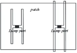
The antenna array element comprises three parts. As depicted in Figure 1: radiating patches, a set of microstrip resonator and a H-slot resonator coupled to the patches for transmitting and the other set of microstrip and H-slot resonators coupled to the patches for receiving. Two same size radiation patches are printed on the top surface of the top substrate and the back of the bottom substrate, respectively. Ground with two different parallel H slots and microstrip resonators are printed on different sides of the middle substrate. Air layers are between the three substrates.
As shown in Figure 1(b), the Tx and Rx ports exploit tap coupling to the microstrip resonators, then the microstrip resonators couple to the patches via the H-slot resonators. The microstrip resonators act as the first stage of the BPFs. And the resonant H slots serve as the coupling structure and the second stage of the BPFs. The radiating patches work as a duplex synthetic cavity. In order to cover both the Tx and Rx bands, wide bandwidth patches are necessary. Bidirectional radiation characteristic is realized by two unidirectional radiating patches. Port 1 operates at center frequency 2.47 GHz for receiving path, and Port 2 operates at center frequency 1.96 GHz for transmitting path.
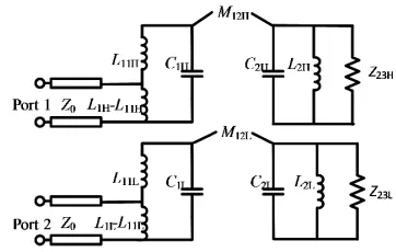
Figure 2 illustrates the equivalent circuit model of the resonators. Both of the microstrip resonators and H-slot resonators are modeled by shuntLC resonators with the same resonant frequency. The microstrip resonators and the H slot resonators are modeled by L1C1 and L2C2, respectively. The coupling between the resonators are expressed by M12. The values of L1, L11, L2, C1, C2 and M12 are expressed by L1H, L11H, L2H, C1H, C2H and M12H when operates at a high band and
L1L, L11L, L2L, C1L, C2L and M12L for the low band. The proposed duplex antenna is designed to
(a) (b)
(c)
Figure 1. Schematics of antenna element. (a) Radiating patch. (b) Feeding network and H-shaped slots. (c) Side view.
operate at 1.96 GHz with 0.3 dB ripple 2.75% fractional bandwidth and 2.47 GHz with 0.3 dB ripple 3.6% fractional bandwidth. Assuming that C1H = 1.33 pF, C2H = 0.53 pF, C1L = 1.53 pF, C2L = 0.64 pF,
Z0 = 50 ohm. Referring to the BPF synthesis technology [13], for a two-order Chebyshev response, the normalized low-pass filter prototype element values are g0 = 1, g1 = 1.18,g2 = 0.696 and g3 = 1.697.
Li = 1 4π2f2
0Ci
, i= 1H,2H,1L,2L (1)
J01 =
Δ2πf0C1
g0g1Z0
(2)
M12 = Δ
√g
1g2
(3)
J23 =
Δ2πf0C2
g1g2Z0
(4)
Z01 = 1
J2 01Z0
(5)
Z23 = 1
J2 23Z0
(6)
Substituting the above values into Eqs. (1)–(6), we can acquire that L1H= 3.1 nH,L2H= 7.8 nH,
L1L = 4.3 nH,L2L = 10.3 nH,Z01H = 1583 ohm,Z01L= 2269 ohm, Z23H = 3961 ohm,Z23L= 5454 ohm,
M12H= 0.0397,M12L= 0.0304. Z01andZ23are the impedance mapped to the I/O ports. A impedance transformation is employed to match the 50 ohm port. At the input port, a tap is set at the resonant coil. The optimizedL11H and L11L is 2.56 nH and 3.65 nH, respectively.
Based on the equal admittance slope, the widths of the corresponding microstrip resonators and H-slot resonators can be determined. Their lengths are all half guiding wavelength at their operating frequencies. The inserting distances ofx direction between the microstrip and H-slot resonatorsd1 and
d2 can be set according to the coupling coefficient M12.
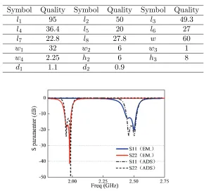
The aperture coupling to the patch can be modeled by the circuit as Figure 3 [14]. The coupling can be treated as a transformer. The ratio of transformation is affected by the width of the patch and the length of the aperture. On the condition of the settled air layers height, varying the sizes of the patches can make the impedance of the H slot coupling patch match the output impedance Z23. The detailed impedance extracting is shown in Figure 4. To verify the model accuracy, the equivalent circuit model and the full-wave simulation S parameter results are compared in Figure 5. The proper geometric parameters are listed in Table 1. It can be seen that the results are well agreed with each other. Note that, all of the three substrates are with dielectric constant 2.55, thickness 0.8 mm, and loss tangent 0.003. The simulated surface currents of the radiating patch at 1.96 GHz and 2.47 GHz are all flowing along x direction, as shown in Figure 6. Thus, same x direction linear polarization waves are able to generate. Figure 7 shows the simulated normalized radiation patterns in E and H planes at 1.96 GHz and 2.47 GHz. The XPD is over 18 dB in bothE plane and H plane at 1.96 GHz and over
Figure 3. Equivalent circuit of the aperture coupling to the patch.
Table 1. Dimensions of designed antenna (unit: mm).
Symbol Quality Symbol Quality Symbol Quality
l1 95 l2 50 l3 49.3
l4 36.4 l5 20 l6 27
l7 22.8 l8 27.8 w 60
w1 32 w2 6 w3 1
w4 2.25 h2 6 h3 8
d1 1.1 d2 0.9
Figure 5. Comparison between full-wave simulation and equivalent circuit model simulation.
(a) (b)
Figure 6. Surface currents of radiating patch at (a) 1.96 GHz, (b) 2.47 GHz.
13 dB in both E plane and H plane at 2.47 GHz. The simulated gains are about 1.7 dBi at 1.96 GHz and 2.65 dBi at 2.47 GHz.
2.2. Antenna Array Design
(a)
(b)
Figure 7. The simulated normalized radiation pattern of the antenna element on E-plane (xz-plane) and H-plane (xy-plane). (a) 1.96 GHz; (b) 2.47 GHz.
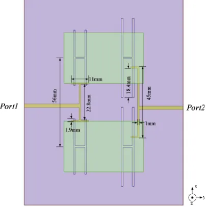
Figure 8. Structure of two-element antenna array.
3. EXPERIMENTAL RESULTS AND DISCUSSIONS
(a) (b) (c)
Figure 9. Antenna prototype. (a) Overall view. (b) Ground view. (c) Feeding network view.
Figure 10. S-parameters of proposed antenna array.
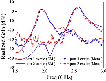
Figure 11. Gain responses of proposed antenna array.
a impedance bandwidth from 2.5 to 2.6 GHz (3.9%) for Port 1 and 1.93–2.03 GHz (5%) for Port 2. Two reflection zeros are obtained at the two bands. There are unexpected dips from 2.2 to 2.4 GHz. The reason is because of the excitation of the high-order modes of the H slots. The small difference between the simulated and measured results is due to fabrication errors. The measured isolation is better than 30 dB between the two ports.
Figure 11 illustrates the full-wave simulated gains in the +Z direction versus frequency for the filtering duplex antenna array. As expected, when Port 1 is excited, the measured broadside maximum gains of the antenna at the transmitting band are 4.85 dBi and drop sharply to below −20 dBi in the receiving band. While Port 2 is excited, the gain is stable with about 2.46 dBi and the suppression at the lower band is below −25 dBi. The results exhibit high-frequency selectivity and good out-of-band rejection. The simulated efficiency is about 71% at 1.98 GHz and 79.6% at 2.55 GHz.
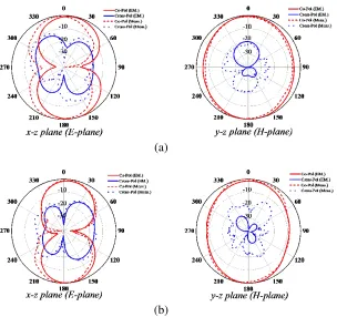
Figure 12 (a) shows that the simulated and measured normalized radiation patterns inφ= 0◦ and
φ= 90◦ planes at 1.98 GHz when Port 2 is excited, whereas Port 1 is terminated with a 50 Ω load. The XPD is over 15 dB in both XOZ plane (φ = 0◦) and Y OZ plane (φ = 90◦). Figure 11(b) shows the normalized simulated and measured co- and cross-polarization radiation patterns of the array in two orthogonal planes at 2.55 GHz when Port 1 is excited and the Port 2 is terminated with a 50 Ω load. The simulated and measured results agree well with each other, exhibiting a maximum radiation in the broadside. The XPD is over 20 dB in XOZ plane (φ= 0◦) and Y OZ plane (φ= 90◦).
(a)
(b)
Figure 12. The simulated and measured normalized radiation pattern of the proposed antenna on
E-plane (xz-plane) andH-plane (xy-plane). (a) 1.98 GHz; (b) 2.55 GHz.
Table 2. Comparison with previous work.
Ref. Frequency space ratio
(fH −fL)/((fH +fL)/2) Size
Radiation Pattern
Isolation (dB)
[10] 0.77 0.9×0.9×0.022λ0 Bidirectional 26
[11] 0.22 0.66×0.66×0.021λ0 Unidirectional 22 [12] 0.74 1.01×2.19×0.026λ0 Unidirectional 20 This work 0.23 0.98×0.75×0.09λ0 Bidirectional 30
4. CONCLUSION
The design of a small Tx-Rx frequency space filtering duplex antenna array has been presented and discussed. The proposed antenna array integrates the coupling feeding network with the filtering structure. Thus, the overall trans-receiver system is compact, low cost and easy to be fabricated. Moreover, small transmitting and receiving frequency space can be accomplished. The relative frequency space r is only 0.23. And more than 30 dB port-to-port isolation is achieved at the transmitting and receiving bands. Besides, the antenna possesses relatively good bidirectional radiation characteristic.
REFERENCES
2. Hanseishi, M. and M. Konno, “Dual-polarized planar antenna fed by dog-bone slots,” IEEE 11th Int. Antenna and Propagation Conf., 45–48, 2001.
3. Row, J. S., “Two-element dual-frequency microstrip antenna with high isolation,” Electron. Lett., Vol. 39, No. 25, 1786–1787, 2003.
4. Chiou, T. W. and K. L. Wong, “Broad-band dual-polarized single microstrip patch antenna with high isolation and low cross polarization,” IEEE Trans. Antennas Propagat., Vol. 50, 399–401, Mar. 2002.
5. Chung, Y., S. S. Jeon, S. Kim, D. Ahn, J. I. Choi, and T. Itoh, “Multifunctional microstrip transmission lines integrated with defected ground structure for RF front-end application,” IEEE Trans. Microw. Theory Tech., Vol. 52, No. 5, 1425–1432, 2004.
6. Tirado-Mendez, J. A., H. Jardon-Aguilar, R. Flores-Leal, M. Reyes-Ayala, and E. Andrade-Gonzalez, “Improving performance of non-duplexer active transceiver antenna with defected structures,”IET Microw. Antennas Propag., Vol. 4, No. 3, 342–352, 2010.
7. Luis, I. S., V. R. Jose-Luis, and R. I. Eva, “High isolation proximity coupled multilayer patch antenna for dual-frequency operation,” IEEE Trans. Antennas Propagat., Vol. 56, No. 4, 1180– 1183, 2008.
8. Hao, Y. and C. G. Paini, “Isolation enhancement of anisotropic UC-PBG microstrip diplexer patch antenna,” IEEE Antennas Wireless Propag. Lett., Vol. 1, No. 1, 135–137, 2002.
9. Fallahzadeh, S., H. Bahrami, A. Akbarzadeh, and M. Tayarani, “High-isolation dual-frequency operation patch antenna using spiral defected microstrip structure,” IEEE Antennas Wirless Propag. Lett., Vol. 9, 122–124, 2010.
10. Lu, Y. C. and Y. C. Lin, “A mode-based design method for dual-band and self-diplexing antennas using double T-stubs loaded aperture,”IEEE Antennas Wireless Propag. Lett., Vol. 60, 5596–5603, 2012.
11. Mukherjee, S. and A. Biswas, “Design of self-diplexing substrate integrated waveguide cavity backed slot antenna,” IEEE Antennas Wireless Propag. Lett., Vol. 15, 1775–1778, 2016.
12. Lee, Y. J., J. H. Tarng, and S. J. Chung, “A filtering diplexing antenna for dual-band operation with similar radiation patterns and low cross-polarization levels,”IEEE Antennas Wireless Propag. Lett., Vol. PP, No. 99, 1–1, 2016.
13. Hong, J. S. and M. J. Lancaster, Microstrip Filters for RF/Microwave Applications, Wiley, New York, 2001.
14. Himdi, M. and J. P. Daniel, “Transmission line analysis of aperture-coupled microstrip antenna,”
Electron. Lett., Vol. 25, 1406–1408, 1989.