Design and Development of High Voltage-Low
Power Impulse Charge Circuit for Single Shot
Industrial Application
Amit Pandey1
Project Associate, Electrical Engineering Department, IIT, Ropar, India1
ABSTRACT:Single shot firing circuits have many industrial and defence applications. Due to its dedicated applications firing circuits must be highly reliable, stable, versatile and cost effective. These characteristics can be achieved with the help of electronic triggering circuit which contains a power converter, storage device, firing switch and an external event triggering pulse. This paper mainly focuses on development of single phase, high voltage, low power isolated DC- DC converter design. A single stage Flyback converter is designed to achieve input to output conversion ratio (1:300) with the given design specifications (Input voltage 5V, Output Voltage 1500V, output capacitor 2.4µfd, Firing time 2Sec). This electronic firing circuit has been implemented, tested and verified on P-SPICE simulation tool along with bread board design.
KEYWORDS:Electronic Triggering, Single shot, SCR Firing, Flyback Transformer.
I.INTRODUCTION
In single shot applications, a device have to perform their function for only once in its life time span. System having single time application can be designed very effectively and cost productively using electrical and electronic components. Figure 1 shows the basic block diagram for electronic firing circuit with major components and given specification:
Fig. 1. Block Diagram of firing circuit
• Input power supply (+5V)
• DC-DC converter- Converts the 5V input to 1500V
• Charge storage Capacitor (2.4uF) - Stores and transfers energy to the load • Firing Input- Generated by external circuit
• Pulse Generation- SCR (Functions as a switch)
As given in the specification input power supply is limited to +5V and 1.5Amp (peak). A DC-DC flyback converter is used to boost output voltage level to desired 1500V. This converter is designed specifically for low power, high output voltage. Storage capacitor (2.4uf, 2KV) is used to store the charge supplied by the power converter. The charge is store in storage device until firing input is provided to the SCR. Whenever an external firing input is provided on SCR‘s gate terminal, SCR turns on and charge stored in capacitor discharge with SCR with required current profile.
Input Supply
DC-DC
converter
Charge
Storage
Firing Input
Pulse Generation
.II.DESIGN SELECTION
There are various topologies available to boost the voltage level up from the input supply voltage to desire supply voltage. Boost and flyback topologies are two most widely known topologies for power supply.
A. Boost Converter
Fig. 2. Boost converter
Figure 2 shows basic element of boost converter which contains an Inductor L, a switch S, a diode D and a charging output capacitor C. When switch (MOSFET) is turned on, voltage across L is equal to input voltage and current through L increases linearly. When the switch is turned off, the inductor current flows through the diode and charges the output capacitor. During the on-time of the transistor the inductance is charged with energy and during the off-time of the transistor this energy is transferred from the inductor through the diode to the output capacitor. For our purpose, this topology is not suitable because maximum step ratio possible with boost converter is 1:6 [2].
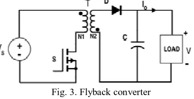
B. Flyback Converter
Flyback topology is generally used to generate multiple input isolated output power supply. Isolated power supply provides better accuracy and safety to other circuit elements. Flyback converters requires very limited external components e.g. a magnetic component at the input and a rectifier at the output terminal.
Fig. 3. Flyback converter
When the switch (MOSFET) is turned ON, and a voltage is applied on the primary winding, the primary current rises linearly. The change of input current is determined by the input voltage, the transformer primary inductance, and the on time. During this time, the energy is stored in the core of the transformer, the output diode D is reverse biased and energy is not transferred to the output load. When the switch is turned off, the magnetic field starts to decrease, which reverses the polarity across the primary and secondary windings. D is forward bias and the energy is transferred to the load [2]. Flyback converter is suitable for our design purpose due to its ability to achieve wide range of conversion ratio.
discontinuous mode has higher peak currents, higher output voltage spikes during the turn-off, faster load transient response, lower primary inductance, smaller transformer size, and reduced EMI noise [1].
In flyback converter, a part of primary inductance which is not coupled with secondary inductance is known as leakage inductance. Leakage inductance reduces the efficiency of the converter and it causes spikes on the drain terminal of the MOSFET (switching device). It can be seen as part of the stored energy that cannot be transferred on the secondary side. To minimize the leakage inductance as much as possible, a snubber circuit is used. It dissipate this additional stored energy from the primary side and prevent switching device to burn off [2].
Flyback topology have major disadvantages as-it needs a high-value output capacitor, the high current stress on the power switch and output diode, high eddy current loss in the air-gap area, a large transformer core, and potential EMI problem [2].
Thyristors or SCR (Silicon controlled Rectifiers), IGBTs (Insulated Gate Bipolar Transistor) along with Transistors and MOSFETs are most widely used power electronics switching devices. SCR and IGBT are mostly used in high power application while BJT and MOSFET have higher switching speed [4-6]. For this particular design, primary side have low power and low voltage specifications which enable us to choose switching speed over power. Input to the switching device is provided in the form of PWM waveform which can be generated by square wave generator or dedicated IC. Voltage controlled switches are very much easier to implement than current controlled switches on PWM waveform. Enable us to use MOSFET as a switch in this converter design.
III. DESIGNING STEPS
Parameter Formula[3]
Output power = ∗
Secondary average Current
=
Primary average Current
= ∗ Primary peak current
, = 2∗
∗ ∗
Secondary peak current
, = 2∗
∗(1− )
Primary RMS current
= ∗√
3 Secondary RMS current
= ∗ (1− )
3 Primary inductance of a flyback transformer
= ∗ ∗ ∗
2∗ Area Product of the Transformer
(K=0.3 for flyback converters) =
∗10
∗ ∗ ∗
Number of turns on primary (The actual number of turns
required is more) =
∗ ∗
So, No. of Primary turns = 1.2
For a flyback converter, the gap length
=. 4∗ ∗ ∗ ∗10 −
μ FFC, called the fringing flux coefficient
= 1 +
Calculating modified number of turns in the primary
winding = ∗
. 4∗ ∗10 ∗ ∗
1) Peak flux density ( )
If Bsat<Bmax then Nm=Nm*(Bmax/Bsat)
. ∗ ∗ ∗ ∗ ∗
+
No. of Secondary Windings
= ∗ ∗(1− )
∗ Wire Cross Sectional area
=
Skin depth:
If the condition diameter (without insulation)<2d, then use Litz wire
= 2∗
∗ μ
(for Litz wire only) Number of strands=
Required Area / Area of single strand
Cross Verification Ʃ( ∗ )≤ ∗
Some given considerations for this design:
Output Voltage (Vs)= 1500V, Output Current (Is) =.002Amp, Frequency(fs)= 60kHz, Duty Cycle= 75%, Current Density (J)= 3 A/mm2 , Material For Transformer Design= 3C94, Flux density of Material (Bm)= .337 Tesla, Utilization factor(Kw)= 0.3.
IV. EXPERIMENTS AND RESULTS
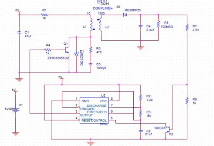
Schematic diagram of the simulated circuit is shown in Figure 4. This circuit is powered by 5V power supply with resistor R1 working as a current limiting resistor. The designed flyback transformer has only two windings, one primary and one secondary windings with inductance L1 & L2 respectively. At the primary side resistor R5, capacitor C5 and diode D1 is used as a snubber circuit to minimize the effect of leakage inductance. 555-Timer IC is used in astable mode to generate a driving waveform of 75% Duty cycle. This fixed duty cycle waveform is used to drive transistor Q1 on regular basis.
At the secondary side diode D2 works as a half wave rectifier which charge storage capacitor up to its desired value. Transistor Q2 helps to shut down the 555Timer IC based driver circuit whenever desired firing voltage is achieved. An SCR can be connected in parallel to load resistor R5 to enable single shot application capability of this circuit.
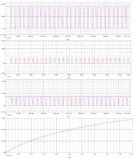
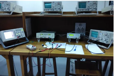
Figure 5 shows P-Spice simulation result of the above circuit. It shows Primary Current (IL1), Secondary Current (IL2), Driving Base Voltage (V33) and Output Voltage (V15) with respect to time.Figure 6 shows the bread board based bench testing of the designed transformer. Test bench results shows desired voltage level of 1.5KV is generated with input power supply of 5V with in stipulated time of 2 Sec. For laboratory test, 5V-1.5Amp power supply is used to power up device.Function generator is used to get square wave with fixed dutycycle of 75% havingrise time (tr) and fall
time (tf) fixed at 100ns. It generate a switching signal equivalent to 555 timer IC in astable mode. At the output side a
high voltage oscilloscope probe (100:1) is used to show the desired output at digital oscilloscope. A voltage divider combination is also used to measure output voltage on digital multimeter.
Fig. 6. Testing of designed transformer
V. CONCLUSION
REFERENCES
[1] George Chryssis, “High-Frequency Switching Power Supply Theory and Design”, McGraw-Hill Publishing Company, Second Edition, 1989. [2] Rashid M. H., Power Electronics, Prentice Hall of India Publishers Ltd., 2009 Sen P. C., Modern Power Electronics, Wheeler Publishing,
1998. Krein P. T., Elements of Power Electronics, Oxford University Press 2003. [3] Cadence Design Systems, Inc. “Magnetic Parts Editor User's Guide”, Product Version 16.3
[4] Basit S. A., Soori P. K., and Omkar M., Heriot Watt University Dubai Campus, Dubai,“Firing Circuit for Converters Used in Drives Applications”, IEEE 7th International Power Engineering and Optimization Conference, Langkawi, Malaysia, DOI 10.1109/PEOCO2013.65644628, June 2013, pp.652-657.
[5] Harada K., Senior Member, IEEE and Saksmoto H., “On the Magnetic Firing Circuit fornan Inverter”, IEEE Transactions On Magnetics, VOL 6, issue 3, DOI:10.1109/TMAG.1970.1066890, April 21-24, pp.658-659.
[6] Simard Remy and Rajagopalan V., Member, IEEE,” Economical Equidistant Pulse Firing Scheme for Thyristorized DC Drives”, IEEE Transactions on Industrial Electronics and Control Instrumentation, Vol. IECI-22, No. 3, August 1975, pp.425-429.
[7] A. B. Shaikh, P. K. Soori, and O. Murthy, “Firing circuit for converters used in drives applications,” in Proc. IEEE 7th International Power Engineering and Optimization Conference, Malaysia, June 2013, pp. 652-657.
[8] Yao-Ching Hsieh, Wei-Guang Chen, Chen-Yao Liu, “Charge-Equalization Circuit for Series-Connected Batteries with Quasi-resonant Flyback Converters", EPE Journal, Volume 20- N°3, September, 2010, p34~39, SCI Journal ISSN 0939- 8368.
[9] S. A. Basit, P. K. Soori and M. Omkar, Heriot Watt University Dubai Campus, Dubai, “Firing Circuit for Converters Used in Drives Applications”, IEEE 7th International Power Engineering and Optimization Conference, Langkawi, Malaysia, pp.652-657, June 2013. [10] K. Subramanian, K. K. Ray, “Synchronised Linear Ramp-Pulse Based Triggering Pulse Generation ON/OFF Control for Solid-State Switches:
Capacitor Switching Applications”, WSEAS Transactions On Power Systems, issue 2, volume 7, April, 2012.
[11] S. A. Zaid, Department of Electrical Power and Machines, Faculty of engineering, Cairo University, “Thyristor Firing Circuit Syncronization Techniques in Thyristor Controlled Series Capacitors”, ICCEP International Conference , pp. 183-188, 2011.
[12] R. M. Usman, “A Universal and Optimized Embedded System to Control Firing Angle of Thyristors with Double-Sided Isolation”, IEEE Third International Conference on Communications and Mobile Computing, pp. 99-102, 2011.