Automated Design, Implementation, and Evaluation of Arbiter-based
PUF on FPGA using Programmable Delay Lines
Mehrdad Majzoobi, Department of Electrical and Computer Engineering, Rice University, Houston, TX, 77005 USA Akshat Kharaya, Department of Electrical and Computer Engineering, Indian Institute of Technology, Powai, Mumbai, MH 400076
Farinaz Koushanfar, Department of Electrical and Computer Engineering, Rice University, Houston, TX, 77005 USA
Srinivas Devadas, Department of Computer Science and Artificial Intelligence Laboratory, Massachusetts Institute of Technology, Cambridge, MA 02142
This paper proposes a novel approach for automated implementation of an arbiter-based physical unclonable function (PUF) on field programmable gate arrays (FPGAs). We introduce a high resolution programmable delay logic (PDL) that is im-plemented by harnessing the FPGA lookup-table (LUT) internal structure. PDL allows automatic fine tuning of delays that can mitigate the timing skews caused by asymmetries in interconnect routing and systematic variations. To thwart the arbiter metastability problem, we present and analyze methods for majority voting of responses. A method to classify and group challenges into different robustness sets is introduced that enhances the corresponding responses’ stability in the face of operational variations. The trade-off between response stability and response entropy (uniqueness) is investigated through comprehensive measurements. We exploit the correlation between the impact of temperature and power supply on responses and perform less costly power measurements to predict the temperature impact on PUF. The measurements are performed on 12 identical Virtex 5 FPGAs across 9 different accurately controlled operating temperature and voltage supply points. A database of challenge response pairs (CRPs) are collected and made openly available for the research community.
Additional Key Words and Phrases: Reconfigurable systems, physically unclonable functions, hardware security, process variation.
1. INTRODUCTION
FPGAs provide a generic substrate of interconnected blocks that can be (re)programmed to achieve the desired functionality. The inherent flexibility of FPGAs compared to Application Specific In-tegrated Circuits (ASICs) together with their lower time-to-market as well as availability of third party IPs, have made them the platform of choice for many applications. Like other systems, FP-GAs demand security and resilience to attacks. In addition, techniques for ensuring IP security are necessary for prevention against piracy and unauthorized access.
A common denominator for many security protocols is the concept of asecret. For example, in public- and private- key cryptography, there is a secret key shared among a limited number of parties. However, permanent storage of keys on FPGA is not straightforward, as FPGAs often do not include nonvolatile on-chip memory. Even when the keys are externally powered or hidden in the bitstream, side channel attacks for extracting the keys have been reported [Moradi et al. 2011].
Physical unclonable functions (PUFs) aim at addressing the shortcomings of the digital key stor-age by relying on the secrets generated by the inherent and unclonable unique mesoscopic character-istics (signatures) of the physical phenomena [Pappu et al. 2002; Gassend et al. 2002]. The physical properties of each device determine a specific mapping between a set ofchallenges(inputs) to a set
ofresponses(outputs). Security protocols take advantage of the unique mappings provided by the
CRPs to authenticate the device and/or its components [Majzoobi et al. 2012].
To date, a number of possible implementations of PUFs on FPGAs based on the unique silicon device-specific variations has been reported [Guajardo et al. 2007; Kumar et al. 2008; Suh and Devadas 2007]. New methods based on the reconfigurability of FPGA inherent delay variations of the PUF that is present even when the device is not configured, is used to configure blank FPGA every time an authentication takes place.
Koushanfar 2007]. However, limitations of the existing PUF implementations on FPGA include the polynomial number of CRPs, high power consumption, response errors, arbiter metastability, and/or the delay imbalances dictated by the routing constraints [Morozov et al. 2010; Majzoobi et al. 2009].
This paper introduces new methodologies that enable automated and stable implementation of an arbiter-based PUF on FPGA. An arbiter-based PUF works by comparing path timings for two routes with the same nominal delay (by design) but with slightly different actual delays (caused by manufacturing variations). To achieve equal nominal delays and to avoid biases, the two routes must be symmetric in shape. We introduce a low-overhead and high-resolution programmable delay line (PDL) implemented by a single lookup table (LUT) on the FPGA. The new PDL is used to tune and calibrate the delay bias caused by asymmetries in signal routing. Furthermore, a symmetric PDL-based switch structure is introduced that is implementable on FPGA. Also, the PDL mechanism can remove biases due to systematic variation effects.
To mitigate arbiter metastability and to achieve a higher robustness, we introduce redundancy and majority voting of the responses. We further present a new method to classify and group challenges into different robustness sets. The challenge classification increases the corresponding responses’ re-silience to environmental variations. Using the measurement data collected from PUFs on 12 FPGA across 9 different temperature and power supply conditions, we quantify the response robustness of each group and investigate the trade-off between response robustness and response entropy. Fi-nally, using the measurement data, correlations between the effect of temperature and power supply variations on the PUF responses is quantified.
Our contributions in this paper are as follows:
— We introduce the first finely tunable PDL mechanism on FPGAs. This PDL can be implemented using single LUT and can achieve a resolution of321 second and a dynamic range of 1 pico-second.
— We demonstrate the first working implementation of arbiter-based PUF on FPGA that can be fully automated1. Our implementation uses the PDLs to adjust for undesired asymmetries that
complicate FPGA realization of delay-based PUFs.
— We demonstrate the evaluation of our arbiter-based PUF across a population of 12 identical FP-GAs. A comprehensive open-source database of 64,000 CRPs per PUF is collected in controlled temperature and power supply settings and tuning conditions.
— The CRP database is thoroughly analyzed to derive optimal tuning levels, quantify response sta-bility, train the PUF model, and reverse engineer the component delays.
— We suggest a new hypothesis that a larger delay difference at the arbiter input leads to a more robust (stable) response. We utilize PUF model building and delay parameter training to classify the challenges by the resulting delay difference at the arbiter input and use this classification to confirm our hypothesis.
— We investigate and quantify the trade-off between response robustness and response entropy (uniqueness). We hypothesize that highly robust responses are more likely to be similar (non-unique) across different PUFs.
— We present a new method, based on the temperature and power supply variations, to partially predict response errors in presence of temperature variations without costly temperature tests. We show that the less costly (controlled) power supply tests can help the response error prediction under temperature variations.
The rest of the paper is organized as follows. In Section 2, we provide a short background on arbiter-based PUF construct as well as methods to implement a PDL. In Section 3, we study the related literature on PDL and PUF implementations on FPGA. In Section 4, we introduce our LUT-based programmable delay line mechanism and show how this construct can help in automated implementation of arbiter-based PUF on FPGA. In Section 5, the method for improving the arbiter
1
results accuracy by majority voting is discussed. Section 6 introduces robust challenge/response classification methodology, whereas in the next Section 7, we investigate the trade-off between response robustness and response uniqueness. In Section 8, measurement and evaluation results taken across various PUFs in different operating conditions are analyzed and presented. Section 9 concludes the paper.
2. BACKGROUND
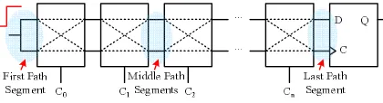
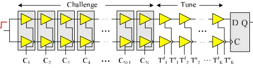
A PUF utilizes the inherent specific properties of a physical device to define a unique mapping from a set of challenges (inputs) to a set of responses (outputs). The delay variations of CMOS logic components can be exploited to produce unique responses. In the PUF structure introduced in [Gassend et al. 2002], the analog delay difference between two parallel timing paths is compared by an arbiter. The paths are built identically and their delays must be equal by construction, but the physical device imperfections make them different. The architecture of thearbiter-based PUF
racing parallel paths is demonstrated in Figure 1. A step input simultaneously triggers the two paths. At the end of the two parallel (racing) paths, an arbiter is used to convert the analog delay difference between the paths to a digital value. The two paths can be divided into several smaller subpaths by inserting path swapping switches. Each set of inputs to the switches act as a challenge set (denoted byCi), defining a new pair of racing paths whose delays can be compared by the arbiter to generate
a one-bit response.
Fig. 1. Arbiter-based PUF with path swapping switches.
2.1. Programmable delay lines
Programmable delay lines (PDLs) alter the signal propagation delay in a controlled fashion. The common mechanisms used to change the delay includes (i) varying the effective load capacitance, (ii) modifying the device current drive (by increasing/decreasing the effective threshold voltage by body biasing), or (iii) incrementally altering the length of the signal propagation path. The first two methods are often employed in either analog fashion and/or in application specific integrated circuits (ASICs) and are not amenable to FPGA implementation.
On reconfigurable digital platforms such as FPGAs, PDLs can be implemented by only chang-ing the signal propagation path length or by alterchang-ing the circuit fanout that modifies the effective load capacitance. The latter is only feasible if dynamic reconfiguration is available. In other words, changing circuit fanout requires topological changes to the circuit which in turn needs a new con-figuration.
3. RELATED WORK
type contain many RO’s so there are many possible pairs to compare. One can only have a quadratic number of challenges with respect to the number of RO’s on FPGAs. Another disadvantage of RO PUF is the continuous dynamic power dissipation due to oscillation.
Another class of candidate FPGA PUFs are SRAM-PUFs and butterfly PUFs [Guajardo et al. 2007; Kumar et al. 2008]. Each FPGA SRAM cell would naturally tend to one logic state (either zero or one) upon startup. There are only a polynomial number of challenges with respect to the number of SRAM cells. An FPGA-based PUF along with a suite of time-bounded authentication protocols is introduced in [Majzoobi et al. 2010b]. The PUF produces binary responses based on the difference between the clock speed and some combinational circuit delay. Some instances of analog and digital PUFs that attempt to implement public cryptography are presented in [Ruhrmair 2009; Beckmann and Potkonjak 2009; Csaba et al. 2009; Jaeger et al. 2010]. A comprehensive survey of PUFs can be found in [U. Ruhrmair 2011].
The scope of previous work on implementation of programmable delay line on FPGA is very limited. Altering the delays is usually performed using hard coded blocks that come ready inside FPGAs or phase locked loops (PLLs). These mechanisms are usually limited to the system clock or subsystem clocks rather than any arbitrary signals. In addition, such blocks provide limited resolu-tions in the order of micro seconds. To the best of our knowledge, the only work that attempts to use FPGA generic components to build programmable delay lines are the work presented in this paper and the one in [Bergeron et al. 2008].
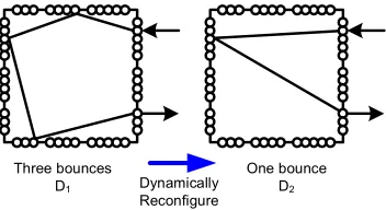
In [Bergeron et al. 2008], a technique is proposed to alter the propagation path length by letting the signal bounce a few times inside the switch matrices of FPGA instead of a direct and straight connection. The concept is illustrated in Figure 2. In the switch matrix on the left side, the signal bounces three times off the switch edges before it exits the switch. In the right switch, the signal only bounces once; as a result a shorter propagation path length and a smaller delay is achieved. However, changing the switch connections points and routings require a new configuration, and doing so during the circuit operation is only possible by dynamic reconfigurability. The experiments on Virtex-II Pro devices show that any differential delay in a range of 947ps can be reached with a precision of +/- 18ps.
Three bounces
D1 Dynamically
Reconfigure
One bounce D2
Fig. 2. A PDL implemented by altering the signal routing inside FPGA switch matrix.
This paper is an extension to the work presented in [Majzoobi et al. 2010c]. It presents a low overhead implementation of a programmable delay line (PDL) mechanism that uses only one look-up table. The proposed PDL can provide a differential delay in range of 10ps with a resolution of a fraction of pico-second without the need for dynamic reconfiguration.
4. ARBITER PUF ON FPGA
symmetry in the PUF layout. However, due to physical constraints of the FPGA fabric, the designer may still not be able to achieve complete symmetry on some routes. Asymmetries in routing when implementing PUFs can lead to bias in delay differences leading to predictable responses, lack of randomness, and decreased response entropy [Majzoobi et al. 2009;?].
The PUF routing can be divided into four different sections; the routing (1) before the first switch, (2) inside the switches, (3) between switches, and (4) after the last switch or before the arbiter (see Figure 1). As we will show later, by placing the logic components on symmetric sites and locations on the FPGA, the routing between switches will automatically follow a symmetric route. However, maintaining acompletesymmetry between the top and bottom path routes before the first switch and after the last switch is structurally infeasible. To alleviate this problem, we introduce and exploit accurate PDLs to tune and remove the bias delay differences caused by asymmetries in net routing. We further introduce a new switch structure that has a symmetric implementation by construction.
4.1. Automated tuning with programmable delay lines
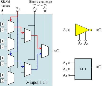
In this section, we introduce a low overhead and high precision PDL withpico-second resolution. The introduced PDL is implemented by a single LUT. Figure 3 shows the internal structure of an example 3-input LUT. Ann-input LUT can be configured to implement anyn-input logic function. The LUT in Figure 3 is configured so that the inputsA2 andA3 act asdon’t-carebits. The LUT
output is invertedA1and is not a function ofA2andA3. However, looking more closely, the inputs A2andA3determine the signal propagation path inside LUT. For instance, ifA2A3= 00, the signal
propagates through the solid path (red), whereas ifA2A3 = 11, the signal propagates through the
path marked with the dashed-lines (blue). The lower dashed path is slightly longer than the upper solid path which results in a larger propagation delay. The Xilinx Virtex 5 FPGA has 6-input LUTs
Fig. 3. The internal structure of a 3-input LUT.
which can implement a PDL with 5 control bits - there are 4 LUTs in each Slice and two Slices per CLB. Similar to the above example, the first LUT input,A1, is the inverter input and the rest
of the LUT inputs control the delay of the inverter. For,A2A3A4A5A6=A[2:6]=00000, the inverter
has the smallest delay (shortest internal propagation path) and forA2A3A4A5A6=A[2:6]=11111,
the inverter has the maximum delay. In general ifA[2:6] > A′[2:6] thenDLU T(A) > DLU T(A′),
whereDLU T(A)andDLU T(A′)are the delay of the inverter withAandA′ as the control inputs
We measured the changes in LUTs’ propagation delays under different inputs. For delay mea-surements, we used the timing characterization circuit shown in Figure 8.1. The characterization circuit consists of alaunchflip-flop,sampleflip-flop, andcaptureflip-flop, an XOR gate, and the
Circuit Under Test (CUT)whose delay is to be measured.
At the rising edge of the clock a signal is sent through the CUT by the launch flip-flop. At the falling edge of the clock, the output of the CUT is sampled by the sample flip-flop. If the signal arrives at the sample flip-flop well before sampling takes place, the correct value is sampled. The XOR compares the sampled value with steady state output of the CUT and produces a zero if they are the same. Otherwise, the XOR output rises to ‘1’, indicating a timing violation. If the signal arrival and the sampling time (almost) simultaneously occur, the sample flip-flop would enter into a metastable condition and produce a non-deterministic output. By sweeping the clock frequency and monitoring the rate at which timing errors happen, the CUT delay can be measured with a very high accuracy and in an automated way. For further details on the delay characterization method the reader is referred to [Majzoobi et al. 2010b].
Fig. 4. Delay characterization circuit.
The measurements performed on Xilinx Virtex 5 FPGAs suggest that the maximum delay differ-ence (i.e.,A=00000, andA′=11111) achieved by each inverter is 9pson average.
4.2. PDL-based symmetric switch
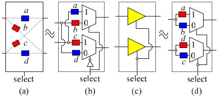
The first arbiter-based PUF introduced in [Gassend et al. 2002] (see Figure 1) uses path swapping switches as shown in Figure 5 (a). The switch, based on its selector bit, provides a straight or cross connection. Figure 5 (b) shows the equivalent circuit implementation and delays. The path swap-ping switch structure does not lend itself to FPGA implementation, since it is extremely difficult to equalize the nominal delays of the top and bottom paths due to routing constraints, i.e.,aandd(or
the diagonal pathsbandc). To alleviate the issue, we propose a new non-swapping switch structure
as shown in Figure 5 (c). The yellow triangles in the figure represent two PDLs. Figure 5 (d) shows its equivalent circuit where the nominal delay values ofaandd(or the diagonal pathsbandc) must
be the same.
The complete PUF circuit that uses the new switch structure and the tuning blocks is shown in Figure 6. The presented system consists of N switches and K tuning blocks. The tuning blocks insert extra delays into either the top or bottom path based on their selector inputs to cancel out the delay bias caused by routing asymmetry. The only difference between a tuning block and a switch block is that in the former, the selectors to the top and bottom PDLs are controlled independently but in the latter, the same selector bit drives both PDLs. Also note that the tuning blocks do not necessarily have to be placed at the end of the PUF. As a matter of fact, they can be placed anywhere on the PUF in between the switches.
The design of this new PUF structure can be readily automated. Similar to the arbiter-based PUF with path swapping switches, the new PUF structure is a linear system. The PUF response will be ‘1’ if the sum of the delay switch differences along the path is greater than zero, and ’0’ otherwise:
N
X
i=1
Ci×(ai−di) + (1−Ci)×(bi−ci) + ∆
R=0
≶
R=10,
(1)
where ai, bi, ci, di are the i-th switch delays as shown in Figure 5 (d),Ci ∈ {0,1} is the i-th
challenge bit, andRis the response. Also,∆is a constant delay difference from the first and last path segments and tuning blocks lumped together. The security aspects of the linear PUF structures against machine learning attacks can be boosted by insertion of feed forward arbiter and attach-ing input/output XOR logic networks to multiple rows of PUFs [Majzoobi et al. 2008; Daihyun et al. 2005]. The work in analyzing the complexity of machine learning and model attacks against different classes of PUFs is given in[Rhrmair et al. 2010].
Fig. 6. The new arbiter-based PUF structure.
5. PRECISION ARBITER
Arbiters in practice are implemented byDflip-flops. As a result, an arbiter has a limited resolution meaning that if the absolute delay difference of the arriving signals is smaller than its setup and/or hold time, it enters a metastable state where its output becomes highly sensitive to circuit noise and will be unreliable. The probability of flip-flop output being equal to ‘1’ is a monotonically decreasing function of the input signal timing difference (∆T). Such probability in fact follows a
Gaussian CDF curve as shown in [Majzoobi et al. 2009; Majzoobi et al. 2010a]:
PO=1(∆T) =Q(
∆T
σ ) (2)
whereQ(x) = √1 2π
R∞
x exp
−u2
2
is theQ function. For an infinitely precise arbiter,σ is infinitesimal i.e.,σ→1/∞, andPO=1(∆T)→1−U(∆T)whereU is the step function.
Fig. 7. Reducing the response instability due to arbiter metastability by using majority voting.
6. ROBUST RESPONSES
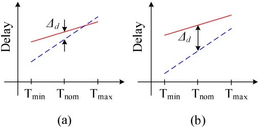
Fluctuations in operational conditions such as temperature and supply voltage can cause variations in device delays. The impact on delays may not be equal on all devices. As an example, the signal propagation delay on the PUF top and bottom paths is represented in Figure 8 by solid and dashed lines respectively. In this example, the path delays increase with temperature at different rates. In the diagram in Figure 8 (a), the delay difference∆dat the end of the PUF for a given applied challenge
at nominal temperature is small, whereas∆d in Figure 8 (b) is larger for another challenge. The
response to the challenge in Figure 8 (a) changes as temperature varies because the delays change their order (cross). However, in Figure 8 (b) the PUF response remains the same. As demonstrated by this example, the responses to those challenges that cause large delay differences are unlikely to be affected by temperature or supply voltage variations [Suh and Devadas 2007].
Fig. 8. Signal propagation delay as a function of temperature.
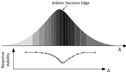
In this paper, we estimate the delay difference at the input of the arbiter. To estimate the cumu-lative delay difference (∆d), we ought to first train the delay parameters of the linear model of the
PUF expressed in Equation 1 on the available set of challenge and responses. After estimating the delay parameters, the left hand sum in Equation 1 is evaluated for every new challenge. The dis-tribution of the resulting sum (∆d) to the set of available CRPs is next calculated. Now based on
Δ
Arbiter Decision Edge
R
e
sp
o
n
se
st
a
b
il
it
y
Δ
Fig. 9. The distribution of∆dand stability of responses in the corresponding partitions.
7. ROBUSTNESS VERSUS ENTROPY
The next question that arises from classifying robust challenges from non-robust ones is: ”Are ro-bust challenges that good?”. In other words, are we trading something off to gain stability and robustness? From information theoretical point of view, it is likely that the responses from more robust challenges bear lower entropy. For example, consider the extreme case where responses are absolutely biased towards either zero or one. In this case we have ultimate robustness whereas the entropy is zero and the responses are not distinct enough for identification. This trade-off (if exists) can only be quantified through measurements. We show this is in fact the case and quantify the loss in entropy in exchange for robustness in the experimental results section.
8. EXPERIMENTAL EVALUATION 8.1. Programmable delay line
Before moving onto the PUF system performance evaluation, we shall first discuss the results of our investigation on the maximum achievable resolution of the programmable delay lines. We set up a highly accurate delay measurement system similar to the delay characterization systems presented in [Majzoobi et al. 2010b; Majzoobi et al. 2010a; Majzoobi and Koushanfar 2011].
The circuit under test consists of four PDLs each implemented by a single 6-input LUT. The delay measurement circuit as shown in Figure 8.1 consists of three flip-flops: launch, sample, and capture flip-flops. At each rising edge of the clock, the launch flip-flop successively sends a low-to-high and high-to-low signal through the PDLs. At the falling edge of the clock, the output from the last PDL is sampled by the sample flip-flop. At the last PDL’s output, the sampled signal is compared with the steady state signal. If the signal has already arrived at the sample flip-flop when the sampling takes place, then these two values will be the same; otherwise they take on different values. In case of inconsistencies in sampled and actual values, XOR output becomes high, which indicates a timing error. The capture flip-flop holds the XOR output for one clock cycle.
To measure the absolute delays, the clock frequency is swept from a low frequency to a high target frequency and the rate at which timing errors occur are monitored and recorded. Timing errors start to emerge when the clock half period (T/2) approaches the delay of the circuit under test. Around this point, the timing error rate begins to increase from 0% and reaches 100%. The center of this transition curve marks the point where the clock half period (T/2) is equal to the effective delay of the circuit under test.
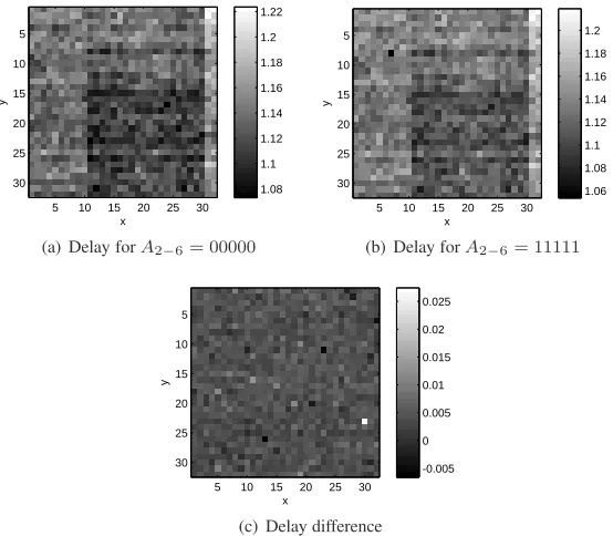
To measure the delay difference incurred by the LUT-based PDL, the measurement is performed twice using different (complementary) inputs. In the first round of measurement, the inputs to the four PDLs are fixed to A2−6 = 11111. In the second measurement, the inputs to the last PDL
are changed toA2−6 = 00000. In our setup, a 32×32 array of the circuit shown on Figure 8.1 is
A2-6=11111 A2-6=00000 A2-6=11111
A2-6=11111 A2-6=11111
1 2 3 4 5 6 1 2 3 4 5 6 1 2 3 4 5 6 1 2 3 4 5 6 D Q clk D Q D Q clk clk Launch Flip-flop Sample Flip-flop Capture Flip-flop L U T -6 L U T -6 L U T -6 L U T -6
Fig. 10. The delay measurement circuit. The circuit under test consists of four LUTs each implementing a PDL.
the two input settings. The clock frequency is swept linearly from 8MHz to 20MHz using a desktop function generator and this frequency is shifted up by 34 times inside the FPGA using the built-in PLL.
The results of the measurement are shown on Figure 11. Each pixel in the image corresponds to one measured delay value across the array. The scale next to the color-map is in nano-seconds. Figure 11 (a) and (b) show the path delay when the last LUT in Figure is driven byA2−6= 00000
andA2−6 = 11111respectively. Figure 11 (c) depicts the difference between the measured delays
in (a) and (b). As can be seen, the delay values in (b) are on average about 10 pico-seconds larger than the corresponding pixel values in (a).
x
y
5 10 15 20 25 30 5 10 15 20 25 30 1.08 1.1 1.12 1.14 1.16 1.18 1.2 1.22
(a) Delay forA2
−6= 00000
x
y
5 10 15 20 25 30 5 10 15 20 25 30 1.06 1.08 1.1 1.12 1.14 1.16 1.18 1.2
(b) Delay forA2
−6= 11111
x
y
5 10 15 20 25 30 5 10 15 20 25 30 -0.005 0 0.005 0.01 0.015 0.02 0.025
(c) Delay difference
Fig. 11. The measured delay of 32×32 circuit under tests containing a PDL with PDL control inputs being set to (a)
A2−6= 00000and (b)A2−6= 11111respectively. The difference between the delays in these two cases is shown in (c).
8.2. Arbiter-based PUF evaluation
the placement and routing of one of the PUF rows. As it can be seen, except for the routing at the beginning and end of the PUF, the rest follows a completely symmetric pattern.
(a) (b)
Fig. 12. Routing and placement of the PUF (a) first segment (b) last segment.
8.3. Measurement setup
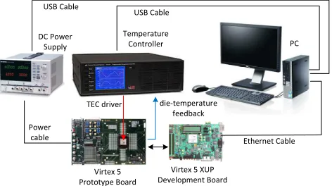
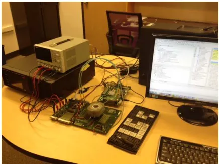
We have a population of 12 Xilinx Virtex 5 (LX110) FPGAs at our disposal. The FPGAs are mounted on a ball-grid array socket available on Xilinx FF676 Prototype board only. Since the prototype board is stripped of any communication interface, we create a synchronous serial commu-nication protocol to send/receive the data to/from XUP-V5 development board. From the XUP-V5 board, the data is sent to the PC through the Ethernet communication interface at a very high speed by using SIRC API. SIRC (Simple Interface for Reconfigurable Computing) is an open sourced software/hardware API developed at Microsoft Research that enables data transfer at full Ethernet speed of 1GB/s between the FPGA and PC [Eguro 2010]. Additionally, to perform measurements under various temperature points, we use PTC10 temperature controller from Stanford Research Systems. The temperature controller drives a TEC (Thermo-electric coupler) Peltier device. TEC is attached on the top of the FPGA and beneath a heat-sink. A closed-loop feedback system is es-tablished to control the FPGA temperature accurately. The temperature feedback is provided by an on-die diode junction voltage on the Virtex 5 device. This way the stable temperature would be that of the die temperature rather than the package temperature. The temperature controller is further calibrated to reliably map the junction voltage of the diode to die temperature using the tempera-ture readings obtained through ChipScope Pro on-die temperatempera-ture sensor. The measurement system connections and setup is depicted in Figure 13. Figure 14 shows the measurement system setup in the lab. The raw data, scripts and software is made available online at http://aceslab.org/node/1012.
Virtex 5 XUP Development Board Virtex 5
Prototype Board
Ethernet Cable USB Cable
USB Cable
DC Power Supply
Temperature
Controller PC
die-temperature feedback TEC driver
Power cable
Fig. 14. Lab setup.
8.4. Tuning the PUF
Before using the PUF, in order to see any changes in the responses it must be tuned to remove the delay bias resulting from routing asymmetry. In the first experiment, we look at all 16 responses to find out at what tuning level their responses to a set of random challenges are 50% zeros and 50% ones. To be able to find the best tuning level, we feed the PUF with a set of 64,000 random challenges while for each challenge, we sweep the tuning level from -10 to 40. In each sweep point (each tuning level), we collect 64,000 responses from each PUF row (64,000×16 total for each FPGA). Then, we look at the percentage of ones and zeros in each response set across different tuning levels and find the set that is properly balanced.
We refer totuning levelas the difference in the number of ‘1’s in the top and bottom PDL selector bits. The tuning level can be either positive or negative indicating insertion of delays to the top and bottom path respectively. Note that when the tuning level is set to 40, for example, then it means that 40 of the PDL blocks out of 64 blocks are dedicated to tuning and only 24 bits of the inputs serve as the input challenge.
The response to a given challenge at each tuning level is repeated 128 times, and a majority vote on the responses is performed to resolve the repeated readings to a single response value. Figure 15 shows the ratios of ones in each response set (y-axis) as a function of tuning level (x-axis) for FPGA number 6. Since each PUF on each FPGA produces 16 response bits, there are 16 lines on each subplot. There are 9 subplots in each plot. Each subplot corresponds to the measurement taken under a different operating condition. The center subplot refers to the normal operating condition (i.e. supply voltageVDD= 1 V and room temperature of 30oC). Note that the plot is only for one
FPGA (FPGA number 6). We have repeated the same experiment on all 12 FPGAs in the lab and the results are available online at http://aceslab.org/node/1012.
Figure 16 shows the distribution of the center of the transition points across all PUFs on all FPGAs.
8.5. Majority voting
-100 0 10 20 30 40 0.2 0.4 0.6 0.8 1 Temp=5C VDD=0.95V Tuning Level Prob{O=1}
-100 0 10 20 30 40
0.2 0.4 0.6 0.8 1 Temp=5C VDD=1V Tuning Level Prob{O=1}
-100 0 10 20 30 40
0.2 0.4 0.6 0.8 1 Temp=5C VDD=1.05V Tuning Level Prob{O=1}
-100 0 10 20 30 40
0.2 0.4 0.6 0.8 1 Temp=35C VDD=0.95V Tuning Level Prob{O=1}
-100 0 10 20 30 40
0.2 0.4 0.6 0.8 1 Temp=35C VDD=1V Tuning Level Prob{O=1}
-100 0 10 20 30 40
0.2 0.4 0.6 0.8 1 Temp=35C VDD=1.05V Tuning Level Prob{O=1}
-100 0 10 20 30 40
0.2 0.4 0.6 0.8 1 Temp=65C VDD=0.95V Tuning Level Prob{O=1}
-100 0 10 20 30 40
0.2 0.4 0.6 0.8 1 Temp=65C VDD=1V Tuning Level Prob{O=1}
-100 0 10 20 30 40
0.2 0.4 0.6 0.8 1 Temp=65C VDD=1.05V Tuning Level Prob{O=1}
Fig. 15. Number of ’1’s in responses (normalized) as a function of tuning level for the PUF on FPGA 6.
-400 -20 0 20 40 10 20 30 40 50 Temp=5C, VDD=0.95V Tuning Level Frequency
-400 -20 0 20 40 10 20 30 40 50 Temp=5C, VDD=1V Tuning Level Frequency
-400 -20 0 20 40 10 20 30 40 50 Temp=5C, VDD=1.05V Tuning Level Frequency
-400 -20 0 20 40 10 20 30 40 50 Temp=35C, VDD=0.95V Tuning Level Frequency
-400 -20 0 20 40 10 20 30 40 50 Temp=35C, VDD=1V Tuning Level Frequency
-400 -20 0 20 40 10 20 30 40 50 Temp=35C, VDD=1.05V Tuning Level Frequency
-400 -20 0 20 40 10 20 30 40 50 Temp=65C, VDD=0.95V Tuning Level Frequency
-400 -20 0 20 40 10 20 30 40 50 Temp=65C, VDD=1V Tuning Level Frequency
-400 -20 0 20 40 10 20 30 40 50 Temp=65C, VDD=1.05V Tuning Level Frequency
-200 -15 -10 -5 0 5 10 15 20 0.2
0.4 0.6 0.8 1
Delay difference (∆ in ps )
Probability of output=1
1 repetition 3 repetitions 5 repetitions 7 repetitions 9 repetitions 11 repetitions
Fig. 17. The probability of majority voting system output being equal to 1 as a function of the delay difference.
The equivalentσwhich represents the width of the metastable window (i.e., 3σ) is calculated for different number of repetitions as shown in Figure 18. The reduction in the metastable window width is logarithmic with respect to the number of repetitions. For 10 repetitions,σ= 2.5ps.
0 2 4 6 8 10 12
2 3 4 5 6 7 8
Number of repetitions
Transition slope (
σ
) in
ps
Fig. 18. The sharpness (σ) of the transition slope versus the number of repetitions for majority voting.
8.6. Robust response classification
0 10 20 0
0.5 1
Bit # 1
Bin Number
Error Rate
0 10 20
0 0.5 1
Bit # 2
Bin Number
Error Rate
0 10 20
0 0.5 1
Bit # 3
Bin Number
Error Rate
0 10 20
0 0.5 1
Bit # 4
Bin Number
Error Rate
0 10 20
0 0.5 1
Bit # 5
Bin Number
Error Rate
0 10 20
0 0.5 1
Bit # 6
Bin Number
Error Rate
0 10 20
0 0.5 1
Bit # 7
Bin Number
Error Rate
0 10 20
0 0.5 1
Bit # 8
Bin Number
Error Rate
0 10 20
0 0.5 1
Bit # 9
Bin Number
Error Rate
0 10 20
0 0.5 1
Bit # 10
Bin Number
Error Rate
0 10 20
0 0.5 1
Bit # 11
Bin Number
Error Rate
0 10 20
0 0.5 1
Bit # 12
Bin Number
Error Rate
0 10 20
0 0.5 1
Bit # 13
Bin Number
Error Rate
0 10 20
0 0.5 1
Bit # 14
Bin Number
Error Rate
0 10 20
0 0.5 1
Bit # 15
Bin Number
Error Rate
0 10 20
0 0.5 1
Bit # 16
Bin Number
Error Rate
Fig. 19. Response stability measured across different challenge partitions with reference to eight operating condition corner
cases for FPGA 6.
Case 1 2 3 4 5 6 7 8 9 10 11 12 13 14 15 16 17 18
T1 L M L L M L L M L M H H M H H M H H
T2 M H H M H H M H H L M L L M L L M L
V1 L L L M M M L L L M M M H H H H H H
V2 M M M H H H H H H L L L M M M L L L
Table 1: 18 correlation cases studies for various increments/decrements on temperature and power supply
Figure 20 shows the distribution of the error rates for each challenge partition using boxplots. Each subplot corresponds to an operating condition corner. As it can be seen, the average error rates is considerably lower at corner (lower and higher) partitions.
8.7. Robustness versus entropy
0 50 100
1 2 3 4 5 6 7 8 91011121314151617181920
Bin
Error Rate (%)
Temp = 5C, VDD = 0.95V
0 50 100
1 2 3 4 5 6 7 8 91011121314151617181920
Bin
Error Rate (%)
Temp = 5C, VDD = 1V
0 50 100
1 2 3 4 5 6 7 8 91011121314151617181920
Bin
Error Rate (%)
Temp = 5C, VDD = 1.05V
0 50 100
1 2 3 4 5 6 7 8 91011121314151617181920
Bin
Error Rate (%)
Temp = 35C, VDD = 0.95V
0 50 100
1 2 3 4 5 6 7 8 91011121314151617181920
Bin
Error Rate (%)
Temp = 35C, VDD = 1.05V
0 50 100
1 2 3 4 5 6 7 8 91011121314151617181920
Bin
Error Rate (%)
Temp = 65C, VDD = 0.95V
0 50 100
1 2 3 4 5 6 7 8 91011121314151617181920
Bin
Error Rate (%)
Temp = 65C, VDD = 1V
0 50 100
1 2 3 4 5 6 7 8 91011121314151617181920
Bin
Error Rate (%)
Temp = 65C, VDD = 1.05V
Fig. 20. Boxplot showing the distribution of error rates for a given operating condition corner and challenge partition.
investigate the Hamming distance for all 12×11 possible pairing (of course excluding similar chip parings). At each partition, a set of 3200 response vectors of size 16 bits are compared to another set. The result is 3200 integer hamming distances between 0 and 16. We take the average value as the inter-chip hamming distance and normalize it with 16. Next we need to link entropy with Hamming distance. Entropy is maximum if the average normalized inter-chip hamming distance is at 0.5. Any deviation from 0.5 lowers the entropy. In other words, both Hamming distance of 0 and 1 indicate entropy of zero. Figure shows the entropy as measured by Hamming distance for response to challenges in each partition. Each line on this figure corresponds to one paring of FPGAs.
8.8. Correlation between effects of temperature and power supply variations
Variation of temperature and/or core voltage from nominal values changes the response to chal-lenges, especially the non-robust challenges. We argue that response flips due to change in temper-ature is related to response flips due to change in core voltage. Tempertemper-ature testing is expensive; if a correlation between variation due to temperature and variation due to core voltage can be estab-lished even partially, it will help predict temperature effects from core voltage effects and thus lead to a huge cost saving.
The 64000x16 responses for each of the 12 FPGA under various experimental conditions (dif-ferent temperature and voltage) are used to quantify this argument. The response set obtained in a reference condition is compared to the response set obtained in conditionN1and the challenges for
which the response flips are noted, whereN1condition being an increment (or decrement) in core
0 5 10 15 20 0
0.05 0.1 0.15 0.2 0.25 0.3 0.35 0.4
CRP Partition Number
Inter-Chip Hamming Distance (Normalized)
Fig. 21. Entropy of the response to the challenges at each robustness partition.
Then the response set obtained in reference condition are compared to the response set obtained inN2condition only for the challenges noted inN1, whereN2condition being an increment (or
decrement) in temperature from the reference value. In other words, if the response to challenge ”C”, flips (changes from 0/1 to 1/0) as the power supply goes fromV1 toV2, how likely is it that
the response to the same challenge ”C”, flips as the temperature goes fromT1 toT2 (while the
core voltage stays atV1). Each PUF is set at a characteristic tuning level for which it has an equal
probability of 0 or 1 as an output and the response set is analyzed at that characteristic tuning level to obtain a response error correlation value. (T1,V1) and (T2,V2) comprise the conditionN1and N2 respectively. Figure 22 shows the results as boxplot for 18 different experimental conditions
tabulated in Table 8.7. The low/high values for core voltage are set assuming a practical tolerance level of 5% in power supply. Low (L), medium (M) and high (H) values for core voltage are 0.95V, 1.00V and 1.05V respectively and for temperature are 5oC, 35oC and 65oC respectively.”
Each box in Figure 22 represents the result of the corresponding case and is drawn for the set response error correlation values obtained from 12×16 PUF response sets. The lower and upper edges represent the 25th and 75th percentile respectively while the edge partitioning the box at the centre is the median correlation value from the set of 192 correlation values which is used to quantify this response error correlation. Correlation between voltage and temperature is maximized in case 16 (0.68355), while the correlation in case 7 is also comparable (0.66355). It is interesting to note that case 16 and case 7 are complementary, i.e. (T1, V1) are interchanged with (T2, V2).
9. CONCLUSION
0 0.1 0.2 0.3 0.4 0.5 0.6 0.7 0.8 0.9 1
1 2 3 4 5 6 7 8 9 10 11 12 13 14 15 16 17 18 Case
Correlation
Fig. 22. The correlation between effect of temperature and power supply variations on responses for 18 different scenarios.
Each box plot is made of response correlation values across 12x16 PUFs.
temperature variations on PUF responses were analyzed and quantified for in-field response error prediction.
REFERENCES
Y. Alkabani, F. Koushanfar, and M. Potkonjak. 2007. Remote activation of ICS for piracy prevention and digital right management. InInternational Conference on Computer Aided Design (ICCAD). 674–677.
Y. M. Alkabani and F. Koushanfar. 2007. Active hardware metering for intellectual property protection and security. In USENIX Security Symposium. 1–16.
N. Beckmann and M. Potkonjak. 2009. Hardware-based public-key cryptography with public physically unclonable func-tions. InIH. 206–220.
E. Bergeron, M. Feeley, M.-A. Daigneault, and J.P. David. 2008. Using dynamic reconfiguration to implement high-resolution programmable delays on an FPGA. InJoint 6th International IEEE Northeast Workshop on Circuits and Systems and TAISA Conference, 2008. NEWCAS-TAISA.265 –268.
Gy¨orgy Csaba, Xueming Ju, Qingqing Chen, Wolfgang Porod, J ¨urgen Schmidhuber, Ulf Schlichtmann, Paolo Lugli, and Ulrich R¨uhrmair. 2009. On-Chip Electric Waves: An Analog Circuit Approach to Physical Uncloneable Functions. Cryptology ePrint Archive(2009).
L. Daihyun, J.W. Lee, B. Gassend, G.E. Suh, M. van Dijk, and S. Devadas. 2005. Extracting secret keys from integrated circuits.IEEE Transactions on Very Large Scale Integration (VLSI) Systems13, 10 (2005), 1200 – 1205.
Ken Eguro. 2010. SIRC: An Extensible Reconfigurable Computing Communication API. InIEEE Annual International Symposium on Field-Programmable Custom Computing Machines (FCCM). 135–138.
B. Gassend, D. Clarke, M. van Dijk, and S. Devadas. 2002. Silicon physical random functions. InCCS. 148–160. J. Guajardo, S. Kumar, G. Schrijen, and P. Tuyls. 2007. FPGA intrinsic PUFs and their use for IP protection. InCHES.
63–80.
C. Jaeger, M. Algasinger, U. Ruhrmair, G. Csaba, and M. Stutzmann. 2010. Random pn-junctions for physical cryptography. Applied Physics Letters96, 17 (2010), 172103 –172103–3.
S.S. Kumar, J. Guajardo, R. Maes, G.-J. Schrijen, and P. Tuyls. 2008. The butterfly PUF protecting IP on every FPGA. In HOST. 67–70.
M. Majzoobi, E. Dyer, A. Elnably, and F. Koushanfar. 2010a. Rapid FPGA Characterzation using Clock Synthesis and Signal Sparsity. InITC.
M. Majzoobi, A. Elnably, and F. Koushanfar. 2010b. FPGA Time-bounded Unclonable Authentication. InIH.
M. Majzoobi and F. Koushanfar. 2011. Time-Bounded Authentication of FPGAs.Information Forensics and Security, IEEE Transactions on6, 3 (sept. 2011), 1123 –1135.
M. Majzoobi, F. Koushanfar, and M. Potkonjak. 2008. Testing Techniques for Hardware Security. InITC. 1–10.
M. Majzoobi, F. Koushanfar, and M. Potkonjak. 2009. Techniques for Design and Implementation of Secure Reconfigurable PUFs.TRETS2, 1 (2009), 1–33.
M. Majzoobi, M. Rostami, F. Koushanfar, D.S. Wallach, and S. Devadas. 2012. Slender PUF Protocol: A Lightweight, Robust, and Secure Authentication by Substring Matching. InIEEE Symposium on Security and Privacy Workshops (SPW). 33 – 44.
Amir Moradi, Alessandro Barenghi, Timo Kasper, and Christof Paar. 2011. On the vulnerability of FPGA bitstream en-cryption against power analysis attacks: extracting keys from xilinx Virtex-II FPGAs. InProceedings of the 18th ACM conference on Computer and communications security (CCS ’11). ACM, New York, NY, USA, 111–124.
S. Morozov, A. Maiti, and P. Schaumont. 2010.An Analysis of Delay BasedPUFImplementations onFPGA. Springer, 382–387.
R. Pappu, B. Recht, J. Taylor, and N. Gershenfeld. 2002. Physical one-way functions.Science297 (2002), 2026–2030. U. Rhrmair, F. Sehnke, J. Slter, G. Dror, S. Devadas, and J. Schmidhuber. 2010. Modeling Attacks on Physical Unclonable
Functions. InConference on Computer and Communications Security.
U. Ruhrmair. 2009. SIMPL system: on a public key variant of physical unclonable function.Cryptology ePrint Archive (2009).
G. Suh and S. Devadas. 2007. Physical Unclonable Functions for Device Authentication and Secret Key Generation. InDAC. 9–14.
G.E. Suh, C.W. O’Donnell, I. Sachdev, and S. Devadas. 2005. Design and implementation of the AEGIS single-chip secure processor using physical random functions. InISCA. 25–36.