Volume 2006, Article ID 46472, Pages1–23 DOI 10.1155/ASP/2006/46472
Rapid VLIW Processor Customization for Signal
Processing Applications Using Combinational
Hardware Functions
Raymond R. Hoare, Alex K. Jones, Dara Kusic, Joshua Fazekas, John Foster, Shenchih Tung, and Michael McCloud
Department of Electrical and Computer Engineering, University of Pittsburgh, Pittsburgh, PA 15261, USA
Received 12 October 2004; Revised 30 June 2005; Accepted 12 July 2005
This paper presents an architecture that combines VLIW (very long instruction word) processing with the capability to introduce application-specific customized instructions and highly parallel combinational hardware functions for the acceleration of signal processing applications. To support this architecture, a compilation and design automation flow is described for algorithms written in C. The key contributions of this paper are as follows: (1) a 4-way VLIW processor implemented in an FPGA, (2) large speedups through hardware functions, (3) a hardware/software interface with zero overhead, (4) a design methodology for implementing signal processing applications on this architecture, (5) tractable design automation techniques for extracting and synthesizing hardware functions. Several design tradeoffs for the architecture were examined including the number of VLIW functional units and register file size. The architecture was implemented on an Altera Stratix II FPGA. The Stratix II device was selected because it offers a large number of high-speed DSP (digital signal processing) blocks that execute multiply-accumulate operations. Using the MediaBench benchmark suite, we tested our methodology and architecture to accelerate software. Our combined VLIW processor with hardware functions was compared to that of software executing on a RISC processor, specifically the soft core embedded NIOS II processor. For software kernels converted into hardware functions, we show a hardware performance multiplier of up to 230 times that of software with an average 63 times faster. For the entire application in which only a portion of the software is converted to hardware, the performance improvement is as much as 30X times faster than the nonaccelerated application, with a 12X improvement on average.
Copyright © 2006 Hindawi Publishing Corporation. All rights reserved.
1. INTRODUCTION
In this paper, we present an architecture and design method-ology that allows the rapid creation of application-specific hardware accelerated processors for computationally inten-sive signal processing and communication codes. The tar-get technology is suitable for field programmable gate arrays (FPGAs) with embedded multipliers and for structured or standard cell application-specific integrated circuits (ASICs). The objective of this work is to increase the performance of the design and to increase the productivity of the designer, thereby enabling faster prototyping and time-to-market so-lutions with superior performance.
The design process in a signal processing or communica-tions product typically involves a top-down design approach with successively lower level implementations of a set of op-erations. At the most abstract level, the systems engineer de-signs the algorithms and control logic to be implemented in a high level programming language such as Matlab or C. This
functionality is then rendered into a piece of hardware, ei-ther by a direct VLSI implementation, typically on eiei-ther an FPGA platform or an ASIC, or by porting the system code to a microprocessor or digital signal processor (DSP). In fact, it is very common to perform a mixture of such implementa-tions for a realistically complicated system, with some func-tionality residing in a processor and some in an ASIC. It is often difficult to determine in advance how this separa-tion should be performed and the process is often wrought with errors, causing expensive extensions to the design cy-cle.
9-bit data or it can executeA∗B+Con 36-bit data in two cycles. An Altera Stratix II contains 72 such blocks as well as numerous logic cells [1]. Xilinx has released preliminary information on their largest Virtex 4 that will contain 512 multiply-accumulate ASIC cells, with 18x18-bit multiply and a 42-bit accumulate, and operate at a peak speed of 500 MHz [2]. Lattice Semiconductor has introduced a low-cost FPGA that contains 40 DSP blocks [3]. From our experiments, a floating point multiplier/adder unit can be created using 4 to 8 DSP blocks, depending on the FPGA.
Additionally, ASICs can contain more computational power than an FPGA but consume much less power. In fact, there are many companies, including the FPGA vendors themselves, that will convert an FPGA design into an equiv-alent ASIC and thereby reduce the unit cost and power con-sumption.
In spite of these attractive capabilities of FPGA architec-tures, it is often intractable to implement an entire applica-tion in hardware. Computaapplica-tionally complex porapplica-tions of the applications, or computational kernels, with generally high available parallelism are often mapped to these devices while the remaining portion of the code is executed with a sequen-tial processor.
This paper introduces an architecture and a design methodology that combines the computational power of application-specific hardware with the programmability of a software processor.
The architecture utilizes a tightly coupled general-purpose 4-way very long instruction world (VLIW) proces-sor with multiple application-specific hardware functions. The hardware functions can obtain a performance speedup of 10x to over 100x, while the VLIW can achieve a 1x to 4x speedup, depending on the available instruction level paral-lelism (ILP). To demonstrate the validity of our solution, a 4-way VLIW processor (pNIOS II) was created based on the instruction set of the Altera NIOS II processor. A high-end 90 nm FPGA, an Altera Stratix II, was selected as the target technology for our experiments.
For the design methodology, we assume that the design has been implemented in strongly typed software language, such as C, or utilizes a mechanism that statically indicate the data structure sizes, like vectorized Matlab. The software is first profiled to determine the critical loops within the pro-gram that typically consume 90% of the execution time. The control portion of each loop remains in software for execu-tion on the 4-way VLIW processor. Some control flow from loop structures is removed by loop unrolling. By using pred-ication and function inlining, the entire loop body is con-verted into a single data flow graph (DFG) and synthesized into an entirely combinationalhardware function. If the loop does not yield a sufficiently large DFG, the loop is considered for unrolling to increase the size of the DFG. The hardware functions are tightly integrated into the software processor through a shared register file so that, unlike a bus, there is no hardware/software interface overhead. The hardware func-tions are mapped into the processor’s instruction stream as if they are regular instructions except that they require mul-tiple cycles to compute. The exact timing of the hardware
functions is determined by the synthesis tool using static tim-ing analysis.
In order to demonstrate the utility of our proposed de-sign methodology, we consider several representative prob-lems that arise in the design of signal processing systems in detail. Representative problems are chosen in the areas of (1) voice compression with the G.721, GSM 06.10, and the pro-posed CCIIT ADPCM standards; (2) image coding through the inverse discrete cosine transform (IDCT) that arise in MPEG video compression; and (3) input multiple-output (MIMO) communication systems through the sphere decoder [4] employing the Fincke-Pohst algorithm [5].
The key contributions of this work are as follows. (i) A complete32-bit 4-way VLIW soft core processor in an
FPGA.Our pNIOS II processor has been tested on a Stratix II FPGA device and runs at 166 MHz.
(ii) Speedupsover conventional approaches through hard-ware kernel extraction and custom implementation in the same FPGA device.
(iii) Ahardware/software interface requiring zero cycle over-head. By allowing our hardware functions direct access to the entire register file, the hardware function can operate without the overhead of a bus or other bot-tlenecks. We show that the additional hardware cost to achieve this is minimal.
(iv) Adesign methodologythat allows standard applications written in C to map to our processor using a VLIW compiler that automatically extracts available paral-lelism.
(v) Tractable design automation techniques for mapping computational kernels into efficient custom combina-tional hardware functions.
The remainder of the paper is organized as follows: we provide some motivation for our approach and its need in signal processing inSection 2. InSection 3, we describe the related work to our architecture and design flow. Our archi-tecture is described in detail inSection 4.Section 5describes our design methodology including our method for extract-ing and synthesizextract-ing hardware functions. Our signal process-ing applications are presented inSection 6including an in depth discussion of our design automation techniques us-ing these applications as examples. We present performance results of our architecture and tool flow in Section 7. Fi-nally,Section 8describes our conclusions with planned fu-ture work.
2. MOTIVATION
the achievable performance of the hardware implementa-tion.
However, signal processing scientists work with software systems to implement and test their algorithms. In general, these applications are written in C and more commonly in Matlab. Thus, to supplement the rich amount of hardware logic in FPGAs, vendors such as Xilinx and Altera have re-leased both FPGAs containing ASIC processor cores such as the PowerPC enabled Virtex II Pro and the ARM-enabled Excalibur, respectively. Additionally, Xilinx and Altera also produce soft core processors Microblaze and NIOS, each of which can be synthesized on their respective FPGAs.
Unfortunately, these architectures have several deficien-cies that make them insufficient alone. Hardware logic is difficult to program and requires hardware engineers who understand the RTL synthesis tools, their flow, and how to design algorithms using cumbersome hardware description languages (HDLs). Soft core processors have the advantage of being customizable making it easy to integrate software and hardware solutions in the same device. However, these processors are also at the mercy of the synthesis tools and of-ten cannot achieve necessary speeds to execute the software portions of the applications efficiently. ASIC core processors provide much higher clock speeds; however, these processors are not customizable and generally only provide bus-based interfaces to the remaining FPGA device creating a large data transfer bottleneck.
Figure 1 displays application profiling results for the SpecInt, MediaBench, and NetBench suites, with a group of selected security applications [5]. The 90/10 rule tells us that on average, 90% of the execution time for an application is contained within about 10% of the overall application code. These numbers are an average of individual application pro-files to illustrate the overall tendency of the behavior of each suite of benchmarks. As seen inFigure 1, it is clear that the 10% of code referred to in the 90/10 rule refers to loop struc-tures in the benchmarks. It is also apparent that multime-dia, networking, and security applications, this includes sev-eral signal processing benchmark applications, exhibit even higher propensity for looping structures to make a large im-pact on the total execution time of the application.
Architectures that take advantage of parallel computation techniques have been explored as a means to support compu-tational density for the complex operations required by dig-ital processing of signals and multimedia data. For example, many processors contain SIMD (single instruction multiple data) functional units for vector operations often found in DSP and multimedia codes.
VLIW processing improves upon the SIMD technique by allowing each processing element parallelism to execute its instructions. VLIW processing alone is still insufficient to achieve significant performance improvements over se-quential embedded processing. When one considers a tradi-tional processing model that requires a cycle for operand-fetch, execute, and writeback, there is significant overhead that occupies what could otherwise be computation time. While pipelining typically hides much of this latency, mis-prediction of branching reduces the processor ILP. A typical
100% 80% 60% 40% 20% 0%
Ex
ecution
time
o
f
loops
Speclnt MediaBench Security NetBench Average for benchmark suite
Loop 1 Loop 4 Loop 2
Loop 5 Loop 3 Loops 6-10
Figure 1: Execution time contained within the top 10 loops in the code averaged across the SpecInt, MediaBench, and NetBench suites, as well as selected security applications [5].
software-level operation can take tens of instructions more than the alternative of a single, hardware-level operation that propagates the results from one functional unit to the next without the need for write-back, fetch, or performance-affecting data forwarding.
Our technique for extracting computational kernels in the form of loops from the original code for no overhead implementation in combinational hardware functions allows the opportunity for large speedups over traditional or VLIW processing alone. We have mapped a course-grain compu-tational structure on top of the fine-grain FPGA fabric for implementation of hardware functions. In particular, this hardware fabric is coarse-grained and takes advantage of ex-tremely low-latency DSP (multiply-accumulate) blocks im-plemented directly in silicon. Because the fabric is combi-national, no overhead from nonuniform or slow datapath stages is introduced.
For implementation, we selected an Altera Stratix II EP2S180F1508C4 in part for its high density of sophisticated DSP multiply-accumulate blocks and the FPGA’s rapidly ma-turing tool flow that eventually permits fine grain control over routing layouts of the critical paths. The FPGA is useful beyond prototyping, capably supporting deployment with a maximum internal clock speed of 420 MHz dependent on the interconnect of the design and on-chip resource utiliza-tion. For purposes of comparing performance, we compare our FPGA implementation against our implementation of the Altera NIOS II soft core processor.
3. RELATED WORK
different representations can be from hardware description languages (HDLs) or software languages such as C, C++, Java, and Matlab.
The HardwareC language is a C-like HDL used by the Olympus synthesis system at Stanford [6]. This system uses high-level synthesis to translate algorithms written in Hard-wareC into standard cell ASIC netlists. Esterel-C is a system-level synthesis language that combines C with the Esterel lan-guage for specifying concurrency, waiting, and pre-emption developed at Cadence Berkeley Laboratories [7]. The SPARK synthesis engine from the UC Irvine translates algorithms written in C into hardware descriptions emphasizing extrac-tion of parallelism in the synthesis flow [8,9]. The PACT be-havioral synthesis tool from Northwestern University trans-lates algorithms written in C into synthesizable hardware de-scriptions that are optimized for low-power as well as perfor-mance [10,11].
In industry, several tools exist which are based on be-havioral synthesis. The Bebe-havioral Compiler from Synop-sys translates applications written in SystemC into netlists targeting standard cell ASIC implementations [12,13]. Sys-temC is a set of libraries designed to provide HDL-like func-tionality within the C++ language for system level synthe-sis [14]. Synopsys cancelled its Behavioral Compiler because customers were unwilling to accept reduced quality of re-sults compared to traditional RTL synthesis [15]. Forte De-sign Systems has developed the Cynthesizer behavioral syn-thesis tool that translates hardware independent algorithm descriptions in C and C++ into synthesizable hardware de-scriptions [16]. Handel-C is a C-like design language from Celoxica for system level synthesis and hardware software co-design [17]. Accelchip provides the AccelFPGA product, which translates Matlab programs into synthesizable VHDL for synthesis on FPGAs [18]. This technology is based on the MATCH project at Northwestern [19]. Catapult C from Mentor Graphics Corporation translates a subset of untimed C++ directly into hardware [20].
The difference between these projects and our technique is that they try to solve the entire behavioral synthesis prob-lem. Our approach utilizes a 4-wide VLIW processor to ex-ecute nonkernel portions of the code (10% of the execution time) and utilizes tightly coupled hardware acceleration us-ing behavioral synthesis of kernel portions of the code (90% of the execution time). We match the available hardware re-sources to the impact on the application performance so that our processor core utilizes 10% or less of the hardware re-sources leaving 90% or more to improve the performance of the kernels.
Our synthesis flow utilizes a DFG representation that in-cludeshardware predication: a technique to convert control flow based on conditionals into multiplexer units that select from two inputs from this conditional. This technique is sim-ilar to assignment decision diagram (ADD) representation [21,22], a technique to represent functional register transfer level (RTL) circuits as an alternative to control and data flow graphs (CDFGs). ADDs read from a set of primary inputs (generally registers) and compute a set of logic functions. A conditional called an assignment decisionthen selects an
appropriate output for storage into internal storage elements. ADDs are most commonly used for automated generation of test patterns for circuit verification [23,24]. Our technique is not limited to decisions saved to internal storage, which imply sequential circuits. Rather, our technique applies hard-ware predicationat several levels within acombinational(i.e., DFG) representation.
The support of custom instructions for interface with co-processor arrays and CPU peripherals has developed into a standard feature of soft-core processors and those which are designed for DSP and multimedia applications. Coprocessor arrays have been studied for their impact on speech coders [25,26], video encoders [27,28], and general vector-based signal processing [29–31].
These coprocessor systems often assume the presence and interface to a general-purpose processor such as a bus. Ad-ditionally, processors that support custom instructions for interface to coprocessor arrays are often soft-core and run a significantly slower clock rates than hard-core processors. Our processor is fully deployed on an FPGA system with detailed post place-and-route performance characterization. Our processor does not have the performance bottleneck as-sociated with a bus interconnect but directly connects the hardware unit to the register file. There is no additional over-head associated with calling a hardware function.
Several projects have experimented with reconfigurable functional units for hardware acceleration. PipeRench [32– 36] and more recently HASTE [37] have explored imple-menting computational kernels on coarse-grained reconfig-urable fabrics for hardware acceleration. PipeRench utilizes a pipeline of subword ALUs that are combined to form 32-bit operations. The limitation of this approach is the require-ment of pipelining as more complex operations require mul-tiple stages and, thus, incur latency. In contrast, we are us-ing non-clocked hardware functions that represent numer-ous 32-bit operations. RaPid [38–42] is a coarse-grain re-configurable datapath for hardware acceleration. RaPid is a datapath-based approach and also requires pipelining. Ma-trix [43] is a coarse-grained architecture with an FPGA like interconnect. Most FPGAs offer this coarse-grain support with embedded multipliers/adders. Our approach, in con-trast, reduces the execution latency and, thus, increases the throughput of computational kernels.
Several projects have attempted to combine a reconfig-urable functional unit with a processor. The Imagine pro-cessor [44–46] combines a very wide SIMD/VLIW processor engine with a host processor. Unfortunately, it is difficult to achieve efficient parallelism through high ILP due to many types of dependencies. Our processor architecture differs as it uses a flexible combinational hardware flow for kernel ac-celeration.
of a single processor and our hardware unit connects directly to all registers in the register file for both reading and writ-ing allowwrit-ing hardware execution with no overhead. These projects also assume that the hardware resource must be re-configured to execute a hardware-accelerated kernel, which may require significant overhead. In contrast, our system configures the hardware blocks prior to runtime and uses multiplexers to select between them at runtime. Addition-ally, our system is physically implemented in a single FPGA device, while it appears that Garp and Chimaera were studied in simulation only.
In previous work, we created a 64-way and an 88-way SIMD architecture and interconnected the processing ele-ments (i.e., the ALUs) using a hypercube network [52]. This architecture was shown to have a modest degradation in per-formance as the number of processors scaled from 2 to 88. The instruction broadcasting and the communication rout-ing delay were the only components that degraded the scala-bility of the architecture. The ALUs were built using embed-ded ASIC multiply-add circuits and were extenembed-ded to include user-definable instructions that were implemented in FPGA gates. However, one limitation of a SIMD architecture is the requirement for regular instructions that can be executed in parallel, which is not the case for many signal processing ap-plications. Additionally, explicit communications operations are necessary.
Work by industry researchers [53] shows that coupling a VLIW with a reconfigurable resource offers the robustness of a parallel, general-purpose processor with the accelerat-ing power and flexibility of a reprogrammable systolic grid. For purposes of extrapolation, the cited research assumes the reconfiguration penalty of the grid to be zero and that de-sign automation tools tackle the problem of reconfiguration. Our system differs because the FPGA resource can be pro-grammed prior to execution, giving us a more realistic recon-figuration penalty of zero. We also provide a compiler and automation flow to map kernels onto the reconfigurable de-vice.
4. ARCHITECTURE
The architecture we are introducing is motivated by four fac-tors: (1) the need to accelerate applications within a single chip, (2) the need to handle real applications consisting of thousands of lines of C source code, (3) the need to achieve speedup when parallelism does not appear to be available, and (4) the size of FPGA resources continues to grow as does the complexity of fully utilizing these resources.
Given these needs, we have created a VLIW processor from the ground-up and optimized its implementation to utilize the DSP Blocks within an FPGA. A RISC instruction set from a commercial processor was selected to validate the completeness of our design and to provide a method of de-termining the efficiency of our implementation.
In order to achieve custom hardware speeds, we enable the integration of hardware and software within the same processor architecture. Rather than adding a customized co-processor to the co-processor’s I/O bus that must be addressed
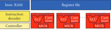
Instr. RAM
Instruction decoder Controller
Register file
ALU Cust.instr.
MUX
ALU Cust.instr.
MUX
ALU Cust.instr.
MUX · · ·
Figure2: Very long instruction word architecture.
through a memory addressing scheme, we integrated the execution of the hardware blocks as if it was a custom in-struction. However, we have termed the hardware blocks as hardware functionsbecause they perform the work of tens to hundreds of assembly instructions. To eliminate data move-ment, our hardware functions share the register file with the processor and, thus, the overhead involved in calling a hard-ware function is exactly that of an inlined softhard-ware functions. These hardware functions can be multiple cycles and are scheduled as if it were just another software instruc-tion. The hardware functions are purely combinational (i.e., not internally registered) and receive their data inputs from the register file and return computed data to the regis-ter file. They contain predication operations and are the hardware equivalent of tens to hundreds of assembly in-structions. These features enable large speedup with zero-overhead hardware/software switching. The following three subsections describe each of the architectural components in detail.
From Amdahl’s Law of speedup, we know that even if we infinitely speedup 90% of the execution time, we will have a maximum of 10X speedup if we ignore the remaining 10% of the time. Thus, we have taken a VLIW architecture as the baseline processor and sought to increase its width as much as possible within an FPGA. An in-depth analysis and perfor-mance results show the limited scalability of a VLIW proces-sor within an FPGA.
4.1. VLIW processor
To ensure that we are able to compile any C software codes, we implemented a sequential processor based on the NIOS II instruction set. Thus, our processor, pNIOS II, is binary-code-compatible to the Altera NIOS II soft-core processor. The branch prediction unit and the register windowing of the Altera NIOS II have not been implemented at the time of this publication.
In order to expand the problem domains that can be im-proved by parallel processing within a chip, we examined the scalability of a VLIW architecture for FPGAs. As shown in Figure 2, the key differences between VLIWs and SIMDs or MIMDs are the wider instruction stream and the shared reg-ister file, respectively. The ALUs (also called PEs) can be iden-tical to that of their SIMD counterpart. Rather than having a single instruction executed each clock cycle, a VLIW can executePoperations for aPprocessor VLIW.
FU FU FU FU FU FU FU FU FU FU FU FU FU FU FU FU
FU FU FU FU FU FU FU FU FU FU FU FU FU FU FU FU
FU FU FU FU FU FU FU FU FU FU FU FU FU FU FU FU
FU FU FU FU FU FU FU FU FU FU FU FU FU FU FU FU
FU FU FU FU FU FU FU FU FU FU FU FU FU FU FU FU
FU FU FU FU FU F FU FU FU FU F FU FU FU FU FU
FU FU FU FU FU F FU FU FU FU U FU FU F FU FU
FU FU FU FU
FU FU FU FU
FU FU FU FU
FU FU FU FU
FU FU FU FU FU FU FU FU FU FU FU U FU FU FU FU
FU FU FU FU FU FU FU FU FU FU FU FU FU FU FU FU
FU FU FU FU FU FU FU FU FU FU FU FU FU FU FU FU
FU FU FU FU FU FU FU FU FU FU FU FU FU FU FU FU
FU FU FU FU FU FU FU FU FU FU FU FU FU FU FU FU
FU FU FU FU FU FU FU FU FU FU FU FU FU FU FU FU
Shared register file Instr. RAM
Instruction decoder Controller
ALU Cust.instr.
MUX
ALU Cust.instr.
MUX
ALU Cust.instr.
MUX
ALU Cust.instr.
MUX
Hardware function Hardware function Hardware function
Hardware function
Hardware function
Hardware function Hardware function Hardware function
Figure3: The VLIW processor architecture with application-specific hardware functions.
then configured in a 4-wide VLIW processor using a shared register file. The shared 32-element register file has 8 read ports and 4 write ports.
There is also a 16 KB dual-ported memory accessible to 2 processing elements (PEs) in the VLIW, and a single 128-bit wide instruction ROM. An interface controller ar128-bitrates between software and hardware functions as directed by the custom instructions.
We targeted our design to the Altera Stratix II EP2-S180F1508C4 FPGA with a maximum internal clock rate of 420 MHz. The EP2S180F has 768 9-bit embedded DSP multiply-adders and 1.2 MB of available memory. The single processor was iteratively optimized to the device based on modifications to the critical path. The clock rate sustained increases to its present 4-wide VLIW rate of 166 MHz.
4.2. Zero-cycle overhead hardware/software interface
In addition to interconnecting the VLIW processors, the reg-ister file is also available to the hardware functions, as shown by an overview of the processor architecture inFigure 3and through a register file schematic inFigure 4. By enabling the compiler to schedule the hardware functions as if they were
software instructions, there is no need to provide an addi-tional hardware interface. The register file acts as the data buffer as it normally does for software instructions. Thus, when hardware function needs to be called, its parameters are stored in the register file for use by the hardware func-tion. Likewise, the return value of the hardware function is placed back into the register file.
The gains offered by a robust VLIW supporting a large instruction set come at a price to the performance and area of the design. The number of ports to the shared register file and instruction decode logic have shown in our tests to be the greatest limitations to VLIW scalability. A variable-sized register file is shown in.
InFigure 4,Pprocessing elements interface toN regis-ters. Multiplexing breadth and width pose the greatest hin-drances to clock speed in a VLIW architecture. We tested the effect of multiplexers by charting performance impact by in-creasing the number of ports on a shared register file, an ex-pression of increasing VLIW width.
O · · ·(P−1) O· · ·(P−1) O · · · (P−1)
Wr sel0 WrMUX0 Wr sel1 WrMUX1 Wr sel(N−1)WrMUX(N−1)
Reg0 Reg1 Reg(N−1)
Wr En0 Wr En1 Wr En(N−1)
RdMUX0 RdMUX1 RdMUX(P−1)
Rd Sel0 Rd Sel1 Rd Sel(P−1)
O· · ·(N−1) O· · ·(N−1) O · · ·(N−1)
Scalable register file
PE0 PE1 PE(P−1)
· · ·
· · ·
· · ·
Figure4:N-element register file supportingP-wide VLIW withPread ports andPwrite ports.
1 0.9 0.8 0.7 0.6 0.5 0.4 0.3 0.2 0.1 0
N
o
rm
aliz
ed
unit
2 4 8 16
Number of processors
two read ports, one write port per processor Area∗VLIW∗
Performance VLIW∗∗ Area VLIW + super CISC∗ Performance VLIW + super CISC∗∗ 257 MHz
226 MHz
197 MHz 249 MHz
12840 ALUT (7%)
24.228 ALUT
(16%) 23.088 ALUT (16%)
91 MHz 69 MHz 2622 ALUT
(1%)
5187 ALUT (3%)
4662 ALUT (3%)
90 MHz
11.149 ALUT (7%) 111 MHz
2593 ALUT (1%)
32-element register file performance and area
Figure 5: Scalability of a 32-element register file forP processors having 2P read andP write ports. Solid lines are for just a VLIW while dashed lines include access for SuperCISC hardware functions. (∗Area normalized as percentage of area of 16 processor register file;
∗∗performance normalized as percentage of performance of 2 processor register file.)
P write ports. As shown, the performance steadily drops and the number of processors is increased. Additionally, the routing resources and logic resources required also increa-ses.
From an analysis of the benchmarks we examined, we found an average ILP between 1 and 2 and concluded that a 4-way VLIW was more than sufficient for the 90% of the code that requires 10% of the time. We also determined that critical path within the ALU was limited to 166 MHz as seen inTable 1. The performance is limited by the ALU and not
the register file. Scaling to 8 or 16-way VLIW would decrease the clock rate of the design, as shown inFigure 5.
Table1: Performance of instructions (Altera Stratix II FPGA EP2S180F1508C4).
Post-place and route results for ALU modules on EP2S180F1508C4
ALUTs % Area Clock Latency
Adder/subtractor/comparator 96 <1 241 MHz 4 ns
32-bit integer multiplier (1 cycle) 0 + 8 DSP units <1 322 MHz 3 ns
Logical unit (AND/OR/XOR) 96 <1 422 MHz 2 ns
Variable left/right shifter 135 <1 288 MHz 4 ns
Top ALU (4 modules above) 416+ DSP units <1 166 MHz 6 ns
1 0.9 0.8 0.7 0.6 0.5 0.4 0.3 0.2 0.1 0
N
o
rm
aliz
ed
unit
4 8 16 32 64 128 256
Number (P) of 32-bit inputs for a singleP-to-1multiplexer Area∗
Performance∗∗ 422 MHz
406 MHz 340 MHz
279 MHz
211 MHz 708 ALUT (<1%) 193 MHz MHz156 171 ALUT
(<1%) 187 ALUT
(1%)
256 ALUT (<1%)
361 ALUT
(<1%) 578 ALUT (<1%)
1326 ALUT (<1%) P-to-1 multiplexer (32 bits) performance and area
Figure6: Scalability of a 32-bitP-to-1 multiplexer on an Altera Stratix II (EP2S180F1508C4). (∗Area normalized as percentage of
256-to-1 multiplexer area;∗∗performance normalized as
percent-age of 4-to-1 multiplexer performance.)
multiplexers increases to implement the read and write ports within the register file.
For anN-wide VLIW, the limiting factor will be the reg-ister file which in turn requires 2N R: 1 multiplexer as each processor reads two registers from a register file withR reg-isters. For the write ports, each of the Rregisters requires an aN : 1 multiplexer. However, as shown inFigure 5, the logic required for a 4-wide VLIW with 32 shared registers of 32-bits each, only achieved 226 MHz while the 32 : 1 multi-plexer achieved 279 MHz. What is not shown is the routing. These performance numbers should be taken as minimums and maximums for the performance of the register file. We were able to scale our VLIW with 32 shared registers up to 166 MHz 4-way.
One technique for increasing the performance of shared register files for VLIW machines is partitioned register files [54]. This technique partitions the original register file into banks of limited connectivity register files that are accessi-ble by a subset of the VLIW processing elements. Busses are used to interconnect these partitions. For a register to be ac-cessed by a processing element outside of the local partition, the data must be moved over a bus using an explicit move instruction. While we considered this technique, we did not employ register file partitioning in our processing scheme for several reasons: (1) the amount of ILP available from our
VLIW compiler was too low to warrant more than a 4-way VLIW, (2) the nonpartitioned register file approach was not the limiting factor for performance in our 4-way VLIW im-plementation, and (3) our VLIW compiler does not support partitioned register files.
4.3. Achieving speedup through hardware functions
By using multicycle hardware functions, we are able to place hundreds of machine instructions into a single hardware function. This hardware function is then converted into logic and synthesized into hardware. The architecture interfaces an arbitrary number of hardware functions to the register file while the compiler schedules the hardware functions as if they were software.
Synchronous design is by definition inefficient. The en-tire circuit must execute at the rate of the slowest component. For a processor, this means that a simple left-shift requires as much time as a multiply. For kernel codes, this effect is mag-nified.
As a point of reference, we have synthesized various arith-metic operations for a Stratix II FPGA. The objective is not the absolute speed of the operations but the relativespeed. Note that a logic operation can execute 5x faster than the entire ALU. Thus, by moving data flow graphs directly into hardware, the critical path from input to output is going to achieve large speedup. The critical path through a circuit is unlikely to contain only multipliers and is expected to be a variety of operations and, thus, will have a smaller delay than if they were executed on a sequential processor.
This methodology requires a moderate sized data flow di-agram. There are numerous methods for achieving this and will be discussed again in the following section. One method that requires hardware support is the predication operation. This operation is a conditional assignment of one register to another based on whether the contents of a third register is a “1.” This simple operation enables the removal of jumps for if-thelse statements. In compiler terms, predication en-ables the creation of large data flow diagrams that exceed the size of basic blocks.
5. COMPILATION FOR THE VLIW PROCESSOR WITH HARDWARE FUNCTIONS
C program
Behavioral synthesis
Profiling C program Trimaran IR Noise IIVLIW
backend Assembly
Noise II VLIW assembler
Machine code
Loops RTL
synthesis
HDL/DFG Bitstream
Figure7: Tool flow for the VLIW processor with hardware functions.
Shark profiling tool from Apple Computer [4] that can pro-file programs compiled with the gcc compiler. Shark is de-signed to identify the computationally intensive loops.
The computational kernels discovered by Shark are prop-agated to a synthesis flow that consists of two basic stages. First, a set of well-understood compiler transformations in-cluding function inlining, loop unrolling, and code motion are used to attempt to segregate the loop control and mem-ory accesses from the computation portion of the kernel code. The loop control and memory accesses are sent to the software flow while the computational portion is converted into hardware functions using a behavioral synthesis flow.
The behavior synthesis flow converts the computational kernel code into a CDFG representation. We use a tech-nique calledhardware predication to merge basic blocks in the CDFG to create a single, larger DFG. This DFG is di-rectly translated into equivalent VHDL code and synthesized for the Stratix II FPGA. Because control flow dependencies between basic blocks are converted into data dependencies using hardware predication, the result is an entirely combi-national hardware block.
The remainder of the code, including the loop control and memory access portions of the computational kernels, is passed through the Trimaran VLIW Compiler [55] for exe-cution on the VLIW processor core. Trimaran was extended to generate assembly for a VLIW version of the NIOS II in-struction set architecture. This code is assembled by our own assembler into machine code that directly executes on our processor architecture. Details on the VLIW NIOS II back-end and assembler are available in [56].
5.1. Performance code profiling
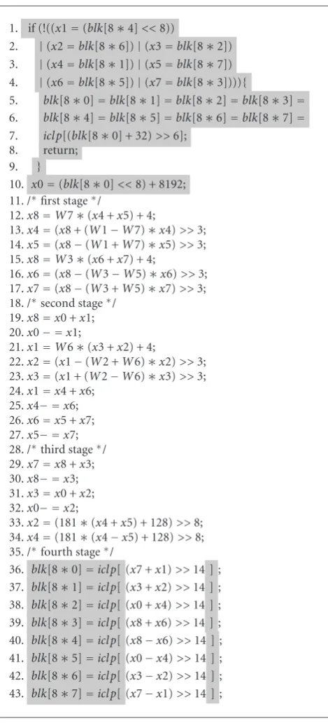
The Shark profiling tool is designed to discover the loops that contribute the most to the total program execution time. The tool returns results such as those seen inAlgorithm 2. These are the top two loops from the G.721 MediaBench bench-mark that total nearly 70% of the total program execution time.
After profiling, the C program is modified to include di-rectives within the code to signal which portions of the code had been detected to be computational kernels during the profiling. As seen inAlgorithm 1, the computational kernel portions are enclosed with the #pragma HW START and #pragma HW END directives to denote the beginning and ending of the kernel, respectively. The compiler uses these directives to identify the segments of code to implement in custom hardware.
predictor zero()
0.80% for (i=1;i <6;i++) /∗ACCUM∗/ 34.60 sezi +=fmult (state ptr−>b[i]>>2,
state ptr−>dq[i]);
-35.40%
quan()
14.20% for (i=0;i <size;i++) 18.10% if (val<∗table++)
1.80% break;
-33.60%
Algorithm1: Excerpt of profiling results for the G.721 benchmark.
1. predictor zero() 2. #pragma HW START
3. for (i=1;i <6;i++) /∗ACCUM∗/ 4. sezi +=fmult(state ptr−>b[i]>>2,
state ptr−>dq[i]); 5. #pragma HW END
6. quan()
7. #pragma HW START 8. for (i=0;i <size;i++) 9. if (val<∗table++)
10. break;
11. #pragma HW END
Algorithm 2: Code excerpt fromAlgorithm 1after insertion of directives to outline computational kernels that are candidates for custom hardware implementation.
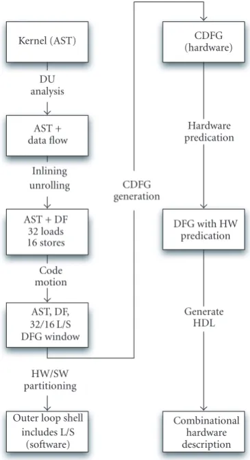
5.2. Compiler transformations for synthesis
Kernel (AST)
DU analysis
AST + data flow
Inlining unrolling
AST + DF 32 loads 16 stores Code motion AST, DF, 32/16 L/S DFG window
HW/SW partitioning
Outer loop shell includes L/S
(software)
CDFG generation
CDFG (hardware)
Hardware predication
DFG with HW predication
Generate HDL
Combinational hardware description
Figure 8: Description of the compilation and synthesis flow for portions of the code selected for custom hardware acceleration. Items on the left side are part of phase 1, which uses standard com-piler transformations to prepare the code for synthesis. Items on the right side manipulate the code further using hardware predication to create a DFG for hardware implementation.
inputs. Sequential logic, on the other hand, requires knowl-edge of timing and prior inputs to determine the output val-ues.
Our synthesis technique only relies on combinational logic synthesis and creates a tractable synthesis flow. The compiler generates data flow graphs (DFGs) that correspond to the computational kernel and, by directly translating these DFGs into a hardware description language like VHDL, these DFGs can be synthesized into entirely combinational logic for custom hardware execution using standard synthe-sis tools.
Figure 8 expands the behavioral synthesis block from Figure 7 to describe in more detail the compilation and synthesis techniques employed by our design flow to gen-erate the hardware functions. The synthesis flow is com-prised of two phases. Phase 1 utilizes standard compiler tech-niques operating on an abstract syntax tree (AST) to decou-ple loop control and memory accesses from the computa-tion required by the kernel, which is shown on the left side ofFigure 8. Phase 2 generates a CDFG representation of the
1. fmult(int an, int srn){ 2. short anmag, anexp, anmant; 3. short wanexp, wanmag, wanmant; 4. short retval;
5. anmag=(an>0) ? an: ((−an) & 0x1FFF); 6. anexp=quan(anmag, power2, 15)−6; 7. anmant=(anmag==0) ? 32:
(anexp>=0) ? anmag>>anexp: anmag<<−anexp;
8. wanexp=anexp + ((srn>>6) & 0xF)−13; 9. wanmant=(anmant∗(srn & 077)+0x30)>>4; 10. retval=(wanexp>=0) ?
((wanmant<<wanexp) & 0x7FFF): (wanmant>>−wanexp); 11. return (((anˆsrn)<0) ?−retval:
retval); 12.}
Algorithm3: Fmult function from G.721 benchmark.
computational code alone and useshardware predicationto convert this into a single DFG for combinational hardware synthesis.
5.2.1. Compiler transformations to restructure code
The kernel portion of the code is first compiled using the SUIF (Stanford University Intermediate Format) Compiler. This infrastructure provides an AST representation of the code and facilities for writing compiler transformations to operate on the AST. The code is then converted to SUIF2, which provides routines for definition-use analysis.
Definition-use (DU) analysis, shown as the first oper-ation inFigure 8, annotates the SUIF2 AST with informa-tion about how the symbol (e.g., a variable from the original code) is used. Specifically, adefinitionrefers to a symbol that is assigned a new value (i.e., a variable on the left-hand side of an assignment) and ause refers to an instance in which that symbol is used in an instruction (e.g., in an expression or on the right-hand side of an assignment). Thelifetimeof a symbol consists the time from thedefinitionuntil the final usein the code.
1. for (i=0;i <6;i++){ 2. // begin fmult
3. fmult an=state ptr−>b[i]>>2; 4. fmult srn=state ptr−>dq[i];
5. fmult anmag=(fmult an>0) ? fmult an: ((−fmult an) & 0x1FFF);
6. // begin quan
7. quan table=power2;
8. for (quani=0; quani <15; quani++) 9. if (fmult anmag<∗quan table++)
10. break;
11. fmult anexp=quani;
12. // end quan
13. fmult anmant=(fmult anmag==0) ? 32: (fmult anexp>=0) ?
fmult anmag>>fmult anexp: fmult anmag<<−fmult anexp; 14. fmult wanexp=fmult anexp +
((fmult srn>>6) & 0xF)−13; 15. fmult wanmant=(fmult anmant∗
(srn & 077)+0x30)>>4; 16. fmult retval=(fmult wanexp>=0) ?
((fmult wanmant<<fmult wanexp) & 0x7FFF): (fmult wanmant>>−fmult wanexp); 17. sezi +=(((fmult anˆfmult srn)<0) ?
−fmult retval : fmult retval);
18. // end fmult
19.}
Algorithm4: G.721 code after function inlining.
Once function inlining is completed, the inner loop is ex-amined for implementation in hardware. By unrolling this loop, it is possible to increase the amount of code that can be executed in a single iteration of the hardware function. The number of loop iterations that can be unrolled is lim-ited by the number of values that must be passed into the hardware function through the register file. In the example fromAlgorithm 4, each loop iteration requires a value loaded from memory,∗quan table, and a comparison with the sym-bol fmult anmag. Because there are 15 iterations, complete unrolling results in a total of 16 reads from the register file. The resulting unrolled loop is shown inAlgorithm 5. Once the inner loop is completely unrolled, the outer loop may be considered for unrolling. In the example, several values such as the array reads must be passed through the register file be-yond the 16 required by the inner loop, preventing the outer loop from being unrolled. However, by considering a larger register file or special registers dedicated to hardware func-tions, this loop could be unrolled as well.
After unrolling and inlining is completed, there is a max-imum of 32 values that can be read from the register file and 16 values that can be written to the register file. The next phase of the compilation flow uses code motion to move all memory loads to the beginning of the hardware function and move all memory stores to the end of the hardware function. This is done so as not to violate any data dependencies dis-covered during definition-use analysis. The loads from the
if (fmult anmag<∗quan table)
quani=0;
else if (fmult anmag<∗(quan table + 1)) quani=1;
else if (fmult anmag<∗(quan table + 2))
quani=2; . . .
else if (fmult anmag<∗(quan table + 14)
quani=14;
Algorithm5: Unrolled inner loop of inlined G.721 hardware ker-nel.
for (i=0;i <6;i++){
quan table array 0=∗quan table;
quan table array 1=∗(quan table + 1);
. . .
quan table array 14=∗(quan table + 14);
state pointerbarrayi=state ptr−>b[i]; state pointerdqarrayi=state ptr−>dq[i]; // Begin Hardware Function
fmult an=state pointerbarrayi >>2; fmult srn=state pointerdqarrayi; if (fmult anmag<quan table array 0)
quani=0;
else if (fmult anmag<quan table array 1) quani=1;
else if (fmult anmag<quan table array 2) quani=2;
. . .
else if (fmult anmag<quan table array 14) quani=14;
. . .
// End Hardware Function }
Algorithm6: G.721 benchmark after inlining, unrolling, and code motion compiler transformations. (Hardware functionality is in plain text with VLIW software highlighted with gray background.)
software while the remaining code is implemented in hard-ware. This distinction is shown inAlgorithm 6, where soft-ware code is highlighted with a gray background.
5.2.2. Synthesis of core computational code
Once hardware and software partitioning decisions are made as described inSection 5.2.1, the portion of the code for im-plementation in hardware is converted into a CDFG rep-resentation. This representation contains a series of basic blocks interconnected by control flow edges. Thus, each basic block boundary represents a conditional branch operation within the original code. Creation of a CDFG representation from a high level language is a well studied technique beyond the scope of this paper. However, details on creation of these graphs can be found in [6].
In order to implement the computation contained within the computational kernel, the control portions of the CDFG must be converted into data flow dependencies. This al-lows basic blocks, which were previously separated by con-trol flow dependency edges to be merged into larger basic blocks which larger DFGs. If all the control flow cies can be successfully converted into data flow dependen-cies, the entire computational portion of the kernel can be represented as a single DFG. As a result, the DFG can be triv-ially transformed into a combinational hardware implemen-tation, in our case using VHDL, and can be synthesized and mapped efficiently into logic within the target FPGA using existing synthesis tools.
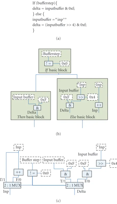
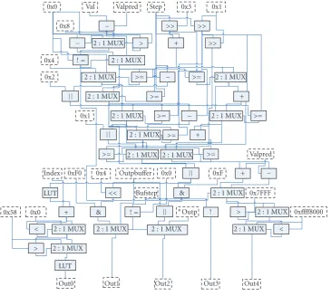
Our technique for converting these control flow depen-dencies into data flow dependepen-dencies is calledhardware pred-ication. This technique is similar to ADDs developed as an alternate behavioral representation for synthesis flows, see Section 3. Consider a traditionalif-then-elseconditional con-struct written in C code. In hardware, an if-then-else con-ditional statement can be implemented using a multiplexer acting as a binary switch to predicated output datapaths. To execute the same code in software, anif-then-elsestatement is implemented as a stream of six instructions composed of comparisons and branch statements.Figure 9shows sev-eral different representations of a segment of the kernel code from the ADPCM encoder benchmark.Figure 9(a)lists the assembly code,Figure 9(b)shows the corresponding CDFG representation of the code segment, andFigure 9(c)presents a data flow diagram for a 2 : 1 hardware predication (e.g., multiplexer) equivalent of the CDFG fromFigure 9(b).
In the example fromFigure 9, thethenpart of the code from Figure 9(a) is converted into the then basic block Figure 9(b). Likewise the statements from theelse portion in Figure 9(a) are converted in into theelse basic block in Figure 9(b). The CDFG inFigure 9(b)shows that the control flow from the if-then-else construction creates basic block boundaries with control flow edges. The hardware predica-tion technique converts these control flow dependencies into data flow dependencies allowing the CDFG in Figure 9(b) to be transformed into the DFG inFigure 9(c). Each sym-bol with a definition in either or both of the basic blocks following the conditional statement (i.e., the thenandelse blocks fromFigure 9(b)) must be predicated by inserting a
If (bufferstep){
delta=inputbuffer & 0xf; }else{
inputbuffer=∗inp++
delta=(inputbuffer>>4) & 0xf; }
(a)
Bufferstep != 0x0
Ifbasic block
Input buffer 0xF & Delta
Thenbasic block
∗Inp Inp
Input buffer 0xF >> 0x4
& ++
Delta Inp
Elsebasic block
(b)
Inp
Input buffer Buffer step
Input buffer
∗Inp
0xF 0xF >> 0x4
++ != 0x0 & &
T/1 F/0
2 : 1 MUX 2 : 1 MUX
Inp
T/1 F/0
Delta (c)
Figure9: Software code, CDFG, and DFG with predicated hard-ware example for control flow in ADPCM encoder.
multiplexer. For example, inFigure 9, the symbol delta is de-fined in both blocks and these definitions become inputs to a rightmost selection multiplexer inFigure 9(c). The symbol inp is updated in theelsebasic block only inFigure 9(b). This requires the leftmost multiplexer in Figure 9(c), where the original value from prior to the condition and the updated value from theelse block become inputs. All of the multi-plexers instantiated due to the conversion of these control flow edges into data flow edges are based on the conditional operation from theif basic block inFigure 9(b).
In many cases, this type of hardware predication works in the general case and creates efficient combinational logic for moderate performance results. However, in some spe-cial cases, control flow can be further optimized for combi-national hardware implementation. In C, switch statements, sometimes called multiway branches, can be handled spe-cially. While this construct can be interpreted in sequence to execute the C code, directly realizing this construct with multiplexing hardware containing as many inputs as cases in the original code allows entirely combinational, parallel execution. A second special case exists for the G.721 exam-ple described inSection 5.2.1. Consider the unrolled inner-most loop shown inAlgorithm 6. This code follows the con-struction if (cond), else if (cond2),. . ., else if (condN). This is similar to the behavior of a priority encoder in combina-tional hardware where each condition has a priority, such as high bit significance overriding lower bit significance. For ex-ample, in a one-hot priority encoder, if the most significant bit (MSB) is “1”, then all other bits are ignored and treated as zeros. If the MSB is “0” and the next MSB is “1”, then all other bits are assumed “0.” This continues down into the least significant bit. When this type of conditional is written in a similar style in synthesizable HDL, synthesis tools will im-plement a priority encoder, just like a case statement in HDL implements a multiplexer. Thus, for the cases where this type of code is present for either the multiplexer or the priority encoder, this structure is retained.
5.3. Interfacing hardware and software
A hardware function can be called with no additional over-head requirements versus that of executing the code directly in software. The impact of even a small hardware/software overhead can dramatically reduce the speedup that the kernel achieves. In essence, some of the speed benefit gained from acceleration is lost due to the interface overhead.
Consider (1), βis thehardware speedup defined as the ratio of software to hardware execution time. This equation only considers hardware acceleration and does not equate di-rectly tokernel speedup. In (2),αis the actual kernel speedup as this considers the portion of the kernel that cannot be translated to hardware. This is labeled as overhead (OH). This definition is actually a misnomer as it implies that there is an added overhead for running our kernel hardware. In fact, this “overhead” is actually the same loads and stores that would be run in the software only solution. No additional computation is added,
β= tsw
thw
, (1)
α= tsw tOH+thw =
β tOH/thw+ 1.
(2)
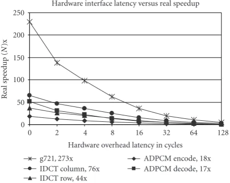
Figure 10shows the effect of adding 0 to 128 cycles of hardware/software overhead on a set of hardware accelerated kernels. We explain how these speedups are achieved later on in this paper and focus here on the impact of data movement overhead. A zero overhead is the pure speedup of the hard-ware versus the softhard-ware. Note that even 2 softhard-ware cycles of
250
200
150
100
50
0
R
eal
speed
up
(
N
)x
0 2 4 8 16 32 64 128
Hardware overhead latency in cycles g721,273x
IDCT column, 76x IDCT row, 44x
ADPCM encode, 18x ADPCM decode, 17x Hardware interface latency versus real speedup
Figure10: Real speedup of hardware benchmark functions com-pared to software execution given varying interface latencies.
Table2: Execution profile of benchmarks.
Execution time of
Benchmark Kernel 1 Kernel 2 Total
ADPCM decode 99.9% N/A 99.9%
ADPCM encode 99.9% N/A 99.9%
G.721 decode 70.5% N/A 70.5%
GSM decode 71.0% N/A 71.0%
MPEG 2 decode 21.5% 21.4% 42.9%
overhead, perhaps caused by a single I/O write and one I/O read, causes the effective kernel speedup to be cut down by a half. For a bus-based system, tens of processor cycles of la-tency dramatically diminish the benefit of hardware acceler-ation. Thus, by enabling direct data sharing through the reg-ister file, our architecture does not incur any penalty.
6. BENCHMARKS
To evaluate the effectiveness of our approach for signal pro-cessing applications, we selected a set of core signal process-ing benchmarks. We examine algorithms of interest in sig-nal processing from three categories: voice compression, im-age and video coding, and wireless communication. The fol-lowing sections describe selected benchmarks in these do-mains and specifically examine benchmark codes selected from each domain. Except for the so-called sphere decoder, the software codes examined in the following sections were taken from the MediaBench benchmark suite [57].
Table3: Instruction level parallelism (ILP) extracted using the Tri-maran compiler.
Instruction level parallelism
Benchmark Kernel 1 Kernel 2 Nonkernel Avg
ADPCM decode
4-way VLIW 1.13 N/A 1.23 1.18
Unlimited VLIW 1.13 N/A 1.23 1.18
ADPCM encode
4-way VLIW 1.28 N/A 1.38 1.33
Unlimited VLIW 1.28 N/A 1.38 1.33
G.721 decode
4-way VLIW 1.25 N/A 1.32 1.28
Unlimited VLIW 1.41 N/A 1.33 1.37
GSM decode
4-way VLIW 1.39 N/A 1.25 1.32
Unlimited VLIW 1.39 N/A 1.25 1.32
MPEG 2 decode
4-way VLIW 1.68 1.40 1.41 1.54
Unlimited VLIW 1.84 1.50 1.46 1.67
and MPEG 2 decoder requires two separate loop kernels to achieve between less than 50% of the execution times.
The ILP of the benchmarks is shown inTable 3. The ILP numbers are broken into three groups, the first being the ILP for the computational kernel of highest complexity (kernel 1), the second for the next highest kernel (kernel 2), which is only necessary for the MPEG 2 benchmark, the ILP of the nonkernel software code, and finally, a nonweighted aver-age ILP for the entire application. All numbers were reported for both a standard 4-way VLIW processor as implemented in our system and compared with numbers for a theoretical unlimited-way VLIW processor.
This limited ILP shows that VLIW processing alone can only provide a nominal performance improvement. The range of speedups possible will be of 20–60% overall, which is far below our target for these applications. To discover how speedups can be achieved through hardware functions in our system, we begin by examining our algorithms, specifically the computational kernel codes below.
6.1. Voice compression algorithms
We chose three representative voice compression algorithms as benchmarks. These were drawn from various applica-tion areas in voice compression and reflect quite different coding algorithms. In each case, the C-language implemen-tation benchmark came from the MediaBench suite. We have purposefully chosen well-established implementations to demonstrate the practical performance gains immediately available to the system designer through our approach.
The first system we examined was the International Con-sultative Committee on Telegraphy and Telephony (CCITT)
G.721 standard, which employs adaptive differential pulse code modulation (ADPCM) to compress toll quality audio signals down to 32kpbs[57]. The G.721 audio compression standard is employed in most European cordless telephones. We next consider CCITT-ADPCM, a different ADPCM implementation that is recommended by the IMA Digital Audio Technical Working Group. The algorithm takes 16 bit PCM samples and compresses them to four bit ADPCM sam-ples, generating a compression ratio of 4 : 1.
The last speech compression algorithm we consider is the GSM 06.10 standard specified for use with the global system for mobile telecommunication (GSM) wireless standard. In the GSM 06.10 standard, residual pulse excitation/long term prediction (RPELTP) is used to encode the speech signal at a compression ratio of 8 : 1. The linear prediction engine runs Schur recursions, which was argued by the package de-signer to yield some performance advantages over the usual Levinson-Durbin algorithm when parallelized [58].
One of the significant bottlenecks of increasing algorith-mic execution is control flow requirements (e.g., determin-ing the next operation to execute based on the result of pre-vious operations). Algorithms high in control flow map very well to sequential processors as these processors are highly optimized to execute these sequential codes by achieving high throughputs and clock speeds through techniques like pipelined execution.
When implementing heavily control-oriented codes in hardware, sequential structures such as finite state machines (FSMs) are often used for this purpose. Unfortunately, these FSMs do not allow significantly more parallelism than run-ning this code in a processor. To achieve a speedup using a VLIW processor it is necessary to attempt to remove the con-trol flow dependencies to allow parallel execution. In sequen-tial processors, predication is used to convert many types of control flow to data flow dependencies.
Consider the ADPCM encoder shown in Algorithm 7. The for loop in the example consumes nearly 100% of the execution time (seeTable 2). Excluding the control flow as-sociated with the for loop, this code segment contains nine (9) conditional executions. These statements are candidates for predication.
To allow predicated execution in a processor, one or more predication registers are used. Conditional branch instruc-tions are traditionally used to executeif statements. To use predication, these branch instructions are replaced by con-ditional operations followed by predicated instructions. For example, inAlgorithm 7, line 7, the subtraction operation is only executed if diff >= step. Thus, the conditional is cal-culated and the result is stored in a predication register. The subtraction instruction can be issued and the result will only be saved if the conditional is true. The same predication reg-ister can also be used for the addition operation in line 8. This type of predication allows increased ILP and reduces stalls in pipelined execution.
1. for ( ; len>0; len–){ 2. val=∗inp++;
3. delta=0;
4. vpdiff=(step>>3); 5. if (diff>=step){ 6. delta=4; 7. diff− =step; 8. vpdiff+=step; 9.}
10. step>>=1; 11. if (diff>=step){ 12. delta| =2; 13. diff− =step; 14. vpdiff+=step; 15.}
16. step>>=1; 17. if (diff>=step){ 18. delta| =1; 19. vpdiff+=step; 20.}
21. if (sign) valpred− =vpdiff; 22. else valpred +=vpdiff; 23. if (valpred>32767) 24. valpred=32767; 25. else if (valpred<−32768) 26. valpred= −32768; 27. delta| =sign;
28. index +=indexTable[delta]; 29. if (index<0) index=0; 30. if (index>88) index=88; 31. step=stepsizeTable[index]; 32. if (bufferstep){
33. outputbuffer=(delta<<4) & 0xf0; 34.}else{
35. ∗outp++= (delta & 0x0f)|outputbuffer; 36.}
37. bufferstep=!bufferstep; 38.}
Algorithm7: ADPCM encoder kernel C code. (Hardware func-tionality is in plain text with VLIW software highlighted with gray.)
For an if statement, both thethenandelseparts of the state-ment are executed and propagated down the DFG based on the result of the conditional. For example, the ADPCM en-coder fromAlgorithm 7was translated into the DFG shown inFigure 11. The blocks labelledMUXimplement the com-binational parallel execution. The conditional operation is used as the selector and the two inputs contain the result of the “predicated” operation as well as the nonmodified result. Two other standard automation techniques were used to convert the code segment into the DFG. First, the load from memory ∗inp from line 2 and the predicated store ∗outp from line 34 ofAlgorithm 7are moved to the begin-ning and end of the DFG, respectively, using code motion. This allows the loads and stores to be executed in software. All code executed in software is highlighted inAlgorithm 7. Secondly the static arrays indexTable and stepsizeTable are
converted into lookup-tables (LUTs) for implementation in ROM structures.
The computational kernel source code for the G.721 benchmark was used in the prior section to describe the var-ious design automation phases. The resulting DFG for the G.721 based on the transformations is displayed inFigure 12. It should be noted that the completely unrolled loop has been transformed into a priority encoder in the hardware imple-mentation. It can also be seen that aside from the encoder, there is only a moderate amount of computations.
6.2. The discrete cosine transform
We next consider a hardware implementation of the inverse discrete-time cosine transform (IDCT). The IDCT arises in several signal processing applications, most notably in im-age/video coding (see, e.g., the MPEG standard) and in more general time-frequency analysis. The IDCT is chosen because there has been a large amount of work on efficient algorithm design for such transforms. Our results argue that further gains are possible with relatively little additional design over-head by employing a mixed architecture.
The IDCT code from the MediaBench suite was ex-tracted from the MPEG 2 benchmark and specifically from the MPEG 2 Decoder used in a variety of applications, most notably for DVD movies. The IDCT actually appears in the JPEG benchmark; however, the implementation from MPEG 2 was selected because it has the longer runtime. The imple-mentation in MPEG 2 decomposes the IDCT into a row-wise and columnwise IDCT.
The IDCT algorithm does a two-dimesional IDCT through decomposition. It first executes a one-dimensional DCT in one dimension (row) followed a one-dimensional DCT in the other (column). The IDCT columnwise decom-position kernel with the software portions highlighted is shown inAlgorithm 8.
Like the IDCT row-wise decomposition, the DFG in Figure 13again contains a significant number of arithmetic functional units and shows a significant amount of paral-lelism.
6.3. The sphere decoder
The last application example we consider is the so-called sphere decoder, which arises in MIMO communication systems. The basic MIMO problem is the following: an M-tupleof information symbolss, drawn from the integer lat-ticeZM, is transmitted fromMtransmit antennas toN re-ceive antennas. We assume that the channel is “flat,” meaning that the fading parameter connecting transmit antennamto receive antennan,hm,n,can be modeled as a scalar, constant over the transmission. The model at the output of a bank of receiver matched filters (one per receive antenna) is simply
y=Hs+n, (3)
0x0 Val Valpred Step 0x3 0x1
0x8 − >> >>
− 2 : 1 MUX > + >> 0x4 != 2 : 1 MUX
0x2 2 : 1 MUX >= − >= 2 : 1 MUX
|| 2 : 1 MUX >= +
0x1 2 : 1 MUX >= − 2 : 1 MUX >= || 2 : 1 MUX >= +
>= 2 : 1 MUX 2 : 1 MUX >= Valpred Index 0xF0 0x4 Outpbuffer 0x0 || 0xF + −
LUT << Bufstep & 2 : 1 MUX 0x7FFF
0x58 0x0 + & != || ∗Outp ! > 2 : 1 MUX 0xffff8000
< 2 : 1 MUX 2 : 1 MUX 2 : 1 MUX 2 : 1 MUX < > 2 : 1 MUX
LUT
Out0 Out1 Out2 Out3 Out4
Figure11: Data flow graph for the ADPCM encoder.
of a real-valued channel model loses no generality since any complex model employing quadrature-amplitude modula-tion (QAM) at the transmitter can be reduced to a real model of twice the dimensions (see, e.g., [59]).
At the receiver we seek to find the inputbwhich mini-mizes the detection norm
s=arg min
s Hs−y
2, (4)
which is generally an exponentially hard problem (i.e., we must considerQMpossible signals when an alphabet of sizeQ is employed). The sphere decoder employs the Fincke-Pohst tree-based search algorithm overZMto reduce this to a de-tection rule which is roughlycubicinMfor sufficiently large
signal-to-noise ratios [60,61]. It is expected to form the core of practical receivers for future MIMO systems.
Unlike the previous algorithms, the spherical decoder was written in vectorized Matlab rather than C. Matlab is a popular language for signal processing algorithm develop-ment because of its native matrix treatdevelop-ment and its built-in mathematical functions. Vectorized Matlab has another nice feature; it is easy to use for extracting parallelism, a main feature for achieving performance improvements by direct hardware implementation.
The code from Algorithm 9 represents the computa-tional core of the spherical decoder, by executing a pointwise
vector multiplication, a vector summation, and finally a dis-tance calculation. The DFG for this function is displayed in Figure 14that includes two square functions and a square-root.
7. RESULTS
To implement our architecture including the hardware func-tions, several industry computer-aided design tools were used to accomplish the functional testing and gate-level syn-thesis tasks of the design flow. We used Mentor Graphics’ FPGA Advantage 6.1 to assist in the generation of VHDL code used to describe the core processor architecture. The processor was built up to support all of the operations de-scribed in the NIOS II instruction set.
0 an 1 0x1fff > −
& 2 : 1 MUX
==
>>
Priority encoder
0 1
−
>= −
0x30 0x4d srn 6 0xf 0xd 4 & >>
+ &
<<
2 : 1 MUX
2 : 1 MUX an srn
0 ∧
<
∗ >= −
+ >>
0
−
0x7fff << &
>>
2 : 1 MUX
−
2 : 1 MUX sezi
Figure12: Resulting DFG from transformations described in G.721 example.
x2 x3 0x0454 0000
0x0a74
0000 x0 x1
0x0b19 0000
0x0235
0000 x4 x5
0x0649 0000
0x0968
0000 x6 x7
+ + − − + + − + − + +
+ +
4 ∗ ∗ ∗ ∗ ∗ ∗ 4 ∗ ∗ ∗ 4
+
− 3 + − 3 + − 3 −
>> >> >> >> >> >>
− + + − − − + +
+ 0xe
>>
blk[7]
+ 0xe
>>
blk[0]
+ 0xb5 0x80 8
∗
+ >>
−
∗
+ >>
+ 0xe − 0xe
>> >>
blk[3] blk[4]
− − + +
>> >> >> >>
blk[6] blk[5] blk[1] blk[2]
0xe 0xe 0xe
![Figure 1: Execution time contained within the top 10 loops inthe code averaged across the SpecInt, MediaBench, and NetBenchsuites, as well as selected security applications [5].](https://thumb-us.123doks.com/thumbv2/123dok_us/1145881.1143788/3.600.319.540.71.238/execution-contained-averaged-specint-mediabench-netbenchsuites-selected-applications.webp)