Pn1 INVERSION. RECTIFICATION, AND CYCIDCONVERSION
Thesis by Khai Doan The Ngo
In Partial Fulfillment of the Requirements for the Degree of
Doctor of Philosophy
California Institute of Technology Pasadena, California
1984
©
1984ACKNOWLEDGEMENTS
,
I would like to thank my advisors, Prof es so rs S. M. Cuk and R. D. Middlebrook for welcoming me to their group at Caltech and bringing me up in Power Electronics. They have offered me the opportunity to explore an area still new and challenging to many of us. They have given me the freedom to select the research direction and to pursue it to our mutual satisfaction. I wish I could contribute more than just this small thesis to deserve their generous givings.
I am indebted to the Office of Naval Research and Naval Ocean Systems Center for their financial supports during the last few years. My special thanks go to Caltech for the Graduate Teaching Assistantships and the President's Fund that initiates research activities in the ac conversion field.
I would like to give credits to other members of the Caltech Power Electronics Group for their contributions to the content and format of this thesis. I am particularly grateful to Mr. X. L. Ma who suggests the six-stepped PWM for the buck rectifier.
ABSTRACT
Topologies and analysis techniques in switched-mode de conversion {d.c-to-dc), inversion (dc-to-ac), rectification (ac-to-dc), and cycloconversion (ac-to-ac) are unified in this thesis. The buck, boost, buck-boost, and ftyback topologies are used to demonstrate that familiar de converters can be extended into equivalent ac converters. Although some of these are presented as fast-switching circuits, they have also been found in slow-switching applications. Thus, topology is the unifying factor not only over four fields of power electronics, but also within each field itself.
Describing equations are used to characterize low-frequency components of the inputs and outputs in fast-switching networks containing filters, excited by de or balanced sinusoidal sources, and
pulse.4.!Jidth.-modulated by de or balanced sinusoidal duty ratios. They are first written in the stationary (abc) reference frame and then transformed to the rotating
(ofb) coordinates. In the ofb coordinates, all balanced ac converters with any number of phases are reduced to a set of continuous, time-invariant differential equations describing a two-phase equivalent.
the four converters are closely related. The cycloconvsrter · is thus
established as the generalized converter that degenerates to the other three under special input and output frequencies.
TABLE OF CONTENTS
ACKNOWLEDGEMENTS iv
ABSTRACT v
INTRODUCTION 1
CHAPI'ER 1 ANALYSIS OF FAST-SWlTCHJNG PWM CONVERTERS 9
1.1 Characterization of the Switch 1 O
1.2 Describing Equations of Fast-Switching PWM Converters 12
1.3 Transformation 20
1.4 Steady-State Analysis 25
1.5 Small-Signal Dynamics 28
1.6 Canonical Model 31
PART I SWITCHED-MODE INVERSION 37
CHAPI'ER 2 REVIEW OF EXISTING INVERTERS 39
2.1 Inverters Switched at Low Frequency 40 2.2 Inverters Switched at Medium Frequency 48 2.3 Inverters Switched at High Frequency 53
CHAPTER 3 FAST-SWITCillNG SINUSOIDAL PWM: INVERTERS 59
3.1 Description of Topologies 60
3.2 Steady-State Performance 74
3.3 Small-Signal Dynamics 79
CHAPTER
4-PART II 4.1 4.2
4.3
4.4
CHAPTER 5 5.1 5.2
CHAPTER 6 6.1 6.2
6.3 6.4
CHAPTER 7
PART Ill 7.1 7.2
7.3
CHAPTER B 8.1 8.2
PRACTICAL ASPECTS 'OF FAST-SWITCIDNG SINUSOIDAL PWM. INVERTERS
Three-Phase Implementation Isolation
Measurement Principle Experimental Verification
SWITCHED-MODE RECTIJi'ICATION
REVIEW OF EXISTING RECTIFIERS Rectifiers Switched at Low Frequency Rectifiers Switched at High Frequency
FAST-SWITCHING SINUSOIDAL PWM RECTIFIERS Description of Topologies
Steady-State Performance Small-Signal Dynamics Canonical Model
PRACTICAL ASPECTS OF FAST-SWITCHING SINUSOIDAL PWM RECTIFIERS
Three-Phase lmplernentation Isolation
Fast-Switching Impedance Converters
SWITCHED-MODE CYCLOCONVERSION
REVIEW OF EXISTING CYCLOCONVERTERS Cycloconverters Switched at Low Frequency Cycloconverters Switched at High Frequency
CHAPTER 9 FAST-SWITCIDNG SJNUSOIDAL PD! CYCLOCONVER'rERs 229
9.1 Description of Topologies 230
9.2 Steady-State Performance 246
9.3 Canonical Model 252
9.4 Reduction of Cycloconverters to
De Converters, Inverters, and Rectifiers 258
CHAPTER 10 PRACTICAL ASPECTS OF FAST-SWITCIDNG
SINUSOIDAL PD CYCLOCONVERTERS 263
10.1 Three-Phase Implementation 263
10.2 Isolation 271
10.3 Fast-Switching Impedance Converters 274 10.4 Experimental Flyback Cycloconverter 277
CONCLUSION
APPENDICES
APPENDIX A A.l
A.2
A.3 A.4
A.5
APPENDIX B
REFERENCES
TOPOLOGY AND ANALYSIS IN DC CONVERSION Description of Topologies
Steady-State Performance Small-Signal Dynamics Canonical Model
Relation of State-Space-Averaging to Describing Equation Technique
THE ABC-OFB TRANSFORMATION
INTRODUCTION
The four areas of switched-mode power conversion are de conversion (de-to-de), inversion (dc-to-ac). rectiff.cation (ac-to-dc). and cycloconversion (ac-to-ac). Although de converters as well as inverters, rectifiers, and cycloconverters have been coexisting for a long time, their applications and advances in semiconductor technology have led them to flourish in different directions. De converters serve delicate and low-power circuits, such as signal-processing ones, that require tight regulation, high-quality outputs, and fast dynamic responses. Owing to these high standards, de power supplies have evolved to a close-to-ideal stage. Inverters. rectifiers, and cycloconverters, on the other hand, encounter more rugged and higher power applications, such as motor drives. that can tolerate poor waveforms and slow dynamic performance. Thus. harmonic heating, torque pulsation, poor power factor, electromagnetic interference, sluggish response, and so
on, have been common problems generated by these high-power units.
converters fall in the low-power range and, hence, enjoy the advantages given by the fast bipolar junction transistor (BJT) and field-effect transistor (FET). High-power ac converters lose these benefits because they can use only the slow thyristor. The performance of medium-power converters, fortunately, has been improved recently owing to progress made in GTO fabrication.
Many advantages of fast switching are apparent from comparison of existing de and ac power processors. First, filters are used more freely because their size diminishes with increasing switching frequency. They attenuate switching harmonics and. hence, smooth out terminal waveforms. They also absorb mismatches between stiff voltage or current sources to suppress excessive current or voltage spikes.
Third, a larger number of topologies introduces a more diversift.ed list of properties that encompass a broader range of applications. Thus, the de gain does not have to be only of buck (step-down), but can also be of boost (step-up) or buck-boost type. Additional control parameters are available so that, for instance, the output amplitude can be adjusted not at the expense of input power factor. Dynamic response can be made very fast by increasing the switching frequency and, consequently, reducing the value of energy-storage components. Isolation is feasible because the isolation transformer is small and economical.
Fourth, it is possible to generate de or sinusoidal waveforms at the input and output of the power processor in an open-loop fashion using only de or sinusoidal control functions. This property is to be distinguished from the S'moothness of waveshape discussed earlier; the de or sinusoidal characteristic describes the low, useful frequency components of the spectrum while the smoothness property refers to the attenuation of switching harmonics. The high-quality output alleviates harmonic stresses at both the load and source, facilitates the understanding of the power stage, and simplifies the design of the overall system.
In the last few decades, the aforementioned attributes have been confined to de converters because a sufficiently fast switch has not been available at the power level of most ac applications. Recently. however, breakthroughs in semiconductor fabrication have improved the speed of the
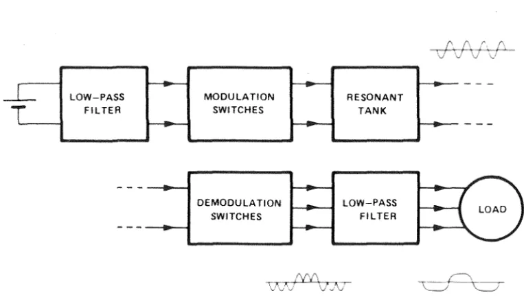
cycloconversion fields. As de conversion, ac conversion can be accomplished by either the resonance or the PWM principle. Although original steps have been reported in both directions, a great deal of fundamental works still need to be done. Since this task certainly takes more than the scope of one thesis, only the PWM area is enlightened here. It is hoped that analogous studies will be carried out for resonance conversion in the near future.
As many other new disciplines, fast-switching PWM ac conversion has started slowly. One of the first efforts parallels many de regulators to create a multiple-input or multiple-output structure [ 19 and 28]. Such an approach has not received much attention because it ignores the polyphase synergism and, hence,
thoughts are put in uses
[37] too
to
many components synthesize genuine,
inefficiently. More basic polyphase cycloconverters that require a minimal amount of switches to synthesize sinusoidal input and output waveforms. Nevertheless, reactive elements are assigned only secondary importance, and their topological /unction ignored. Because of this de-emphasis of the role of inductors and capacitors, [37] fails to discover a host of more useful ac-to-ac converters. Therefore, a. unified, complete picture that describes basic and derived PWM topologies in all four areas of switched-mode conversion, explains their performance systematically, and displays their relationship still needs to be proposed.
introduced recently in [ 1] for circuits without (or with negligible) filter components. Regrettably, it does not cover most practical cases in which filter corners, placed sufficiently low to attenuate the switching noise, do interfere with steady-state as well as dynamic performances. Therefore, a. generalized analysis technique that represents with improved accuracy the steady-state and. dynamic behaviors
o/
/a.st-switching PWM de converters, inverters, rectifiers, a.nd. cycloconverters still needs to be established.Fortunately, the describing equation technique [ 10] has been devised for slow-switching ac converters. Since this method is very general. it applies to fa.st-switching PWM de and a.c networks as well. Describing equation is thus the unified analysis technique over all areas of power electronics and all ranges of switching frequency. Accuracy depends, of course, on the switching strategy, e.g., six-stepped, PWM, or something else.
The preceding two paragraphs embody the overall objectives of this thesis. The details of these objectives are:
to revise analysis techniques for fast-switching PWM converters: to describe fa st-switching open-loop
inverter topologies that invert a de input into sinusoid.al
balanced polyphase outputs,
rectifier topologies that rectify sinusoidal balanced polyphase inputs into a de output, and
cycloconverter topologies that convert sinusoidal balanced polyphase inputs into sinusoidal balanced polyphase outputs
to establish a topalogica.l relationship among de converters, inverters. rectifiers, and cycloconverters.
Most important in the above are the open-loop and sinusoid.al control constraints imposed upon the power processors destined to generate ideal inputs and outputs. These strict criteria exclude the simplistic use of topologies with distorted outputs, for sinusoidal inputs, and then relying on feedback loops to suppress nonlinear harmonics. This thesis proposes to solve a more fundamental problem: to search for open-loop switched-mode networks that require only easy-to-synthesize sinusoidal functions to produce de or sinusoidal quantities. Closed-loop operation is reserved to regulate, not to purify, output waveforms.
Since the analysis technique is universal to all fast-switching PWM converters whose useful bandwidth is restricted sumciently below the switching frequency, it is discussed first in Chapter 1 without reference to any class of circuits. The describing equati.on method is established as the standard modeling procedure for the rest of the thesis. A procedure to derive the describing equations of a switched network is explained, and subsequent manipulations of these equations toward steady-state, dynamic, and canonical models investigated.
switch implementation, isolation, bidirectionality of power flow, impedance conversion, measurement principle, and so on, and verifies experimentally the theory predicted in the previous chapter.
CHAPfER 1
ANALYSIS OF FAST-SWITCHING PW1I CONVERTERS
This chapter consists of six sections. The first section reviews the characterization of a switch: its throws, switching functions, and duty
ratios. The second section derives the describing equations of a switched-mode converter which identify duty ratios as control parameters. The third section transforms these equations to a new coordinate system in which all balanced polyphase ac circuits are represented by their de equivalents. The last three sections then solve the transformed, time-invariant equations for their steady-state formulas. perturb them for their small-signal dynamics, and linearize them for their canonical model.
1.1 Characterization of the Switch
Unlike many de converters, which have only one double-throw switch, most polyphase ac converters contain two or more multiple-throw switches. Ac structures are thus more difficult to comprehend unless their switches are characterized in a systematic manner. Hence, this section is dedicated to the specification of a switch. To start. "switch" in this study is not used interchangeably for "transistor" as in the literature; instead. it simply refers to the device described below.
As is delineated in Fig. 1.1, an N-thraw switch consists of N throws that connect pole w to terminals 1, ... , k, ... , and N in each switching period. The operation of each throw is specified by the switching function
•
dw/t: , where asterisk (•) denotes switching function, which is one when the throw is closed and zero when the throw is open; the set of switching functions for the switch of Fig. 1.1 is illustrated in Fig. 1.2. A switch thus
satisfies two constraints: only one switching function is high, and all switching functions must add up to one at any instant. The first constraint means that the position of the pole is always determinate while that of a throw is not. In other words, the pole is always connected to one of the N throws while a throw may be attached to nowhere. Hence, the open end of an inductor, whose current must ft.ow somewhere, must be assigned to the pole, not a throw, of a switch.
•
The average of the switching function dw1t: over each period Ts is the duty ratio dw/t:. If
dw1t:
varies at a frequency sufficiently slower than the switching frequency, it can be approximated to the continuous law-frequencyF'ig. 1.1 N-throw switch connecting pole w to positions 1, .... k, ... , N.
the second constraint in the previous paragraph, all duty ratios
ot
the same switch should add up to one:N
2::
d'Wk=
1k=l ( 1.1)
Therefore, at most (N-1)
ot
the N throws can be controlled independently. In summary, a multiple-throw switch can be characterized by its s'Witching functions and duty ratios. The switching function, either one or zero, describes the on or off state of each throw. The duty ratio is the average of the switching function over a switching period; there are (N-1)independent duty ratios for an N -throw switch.
1.2 Describing Equations of Fast-Switching PW1I Converters
This section first obtains the switching equations of a general switched network, which can be of resonance, PWM, or any other type. The restriction to PWM is then invoked to derive the describing equations of fast-switching PWM converters.
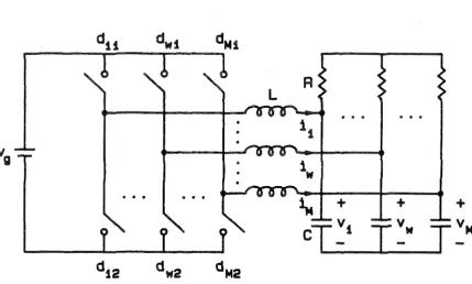
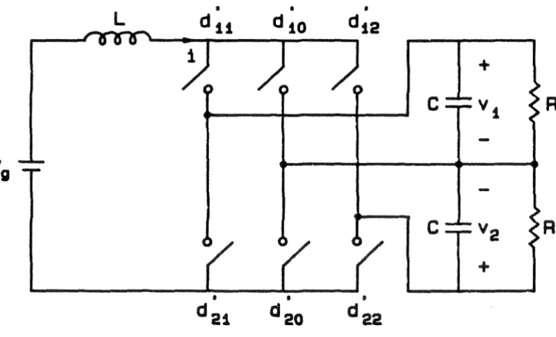
As an example, consider the M-phase boost inverter illustrated in Fig. 1.3. This circuit consists of two M -throw switches that invert the inductor current. supplied by the de source, into polyphase currents driving an M-phase RC load. Note that the switch arrangement is classified as two M-throw, not M double-throw, switches so that the current in the inductor always has some place to ft.ow to. Correct classification is essential in later assignment of modulations to the throws. States in the network are the
.• d 1 • h ()
L
d 11
••
d 1w
••
d1M
••
+
R
. .
.
.
.
.
vg
. . .
+
+
+
•
*
•
2
c1~1
r:·
r:M
••
d21
d2w
••
d2M
••
Pig. 1. 3 M-phase boost inverter with two M-throw switches
pulse4.1Jid.th-mod.ulated. by sinusoid.al functions.
Ir the common or the capacitors is selected as reference point, then the voltage at the upper pole is
and at the lower pole is
are operated.
Application of Kirchhoff's voltage law around the loop containing the source. inductor. and switches yields the following exact state-space switching equation for the inductor:
( 1.2)
••
••
where i means "the first time derivative of t ." Note that this result is
independent of the choice of reference point. The analogous equation for the capacitor is
lswsM
( 1.3}
In the above. the inductor current is switched into the capacitor via the first term, and the resistor current is drawn out by the second term.
In general, a switched-mode converter contains S switches, each of Tm throws, where 1 s m s S. The number of controllable throws Tc is
then
Tc
( 1.4)
•
If Tc independent switching functions dn (just for compactness, only one, instead of two, subscript is used to identify each switching function), where 1
s
ns
Tc. are assigned to these Tc independent throws, the exact state-space switching equation of an ideal converter can be expressed asT
. • c • •
Px
=
l:
d,.,, (Anx +Snu)where
1 ( 1.6)
•
x is the Qx 1 state vector (denoted by boldface), P is the QxQ LC matrix (denoted by boldface),
Ari.
is the QxQ constant matrix,u is the RX 1 source vector,
Bn,
is the QxR constant matrix,and the terms with subscript 0 account for the dependent throws in the topology. Equations ( 1.2) and ( 1.3) can be cast in the form or Eq. ( 1.5) if desired.
Equation ( 1.5) is exact and general in the sense that no particular
mode of control has been specified for the switching function ~ •. It is
difficult to analyze because the switching functions are only piecewise continuous. Nevertheless, it does reduce to a manipulable form for those converters of the fast-switching PWM family.
By definition, the sources and duty ratios of a fast-switching PWM
•
switching function
d.n.
can be approximated by its duty ratio '4i, ; a.nd the•
exact state vector
x
by the principal componentx
of its "Fourier series."Within a modeling bandwidth sufficiently lower than the switching frequency
and a modeling error sufficiently small, then, the useful, low-frequency
variables of the system represented by Eq. ( 1.5) are related by the following
describing equation:
Px
=
2:
Tcd.n.
(Anx+En
u)n=O (1. 7)
where asterisks have been dropped in going from the exact switching to the
low-frequency describing equation. A more compact form of Eq. ( l. 7) is
Px
=
Ax+
Bu
where
Tc
and B
( 1.8)
A=
2:
dnAn
n=O (1.9a,b)
A comparison of Eqs. ( 1.5) and ( 1. 7) reveals that they are similar in
form, the only difference being the asterisks in the former. Therefore, the
two steps are essentially one. and the describing equation can be obtained
expediently by inspection of the topology and use of basic definitions of
circuit elements, Kirchhoff's laws, principle of superposition, and so on.
Note, however, that the describing equation is continuous and, hence, more
tractable than the switching equation.
It is obvious from the describing equation that only duty· ratios, not exact switching details, infiuence the low-frequency behavior of fast-switching
duty ratio, there is no unique switching strategy to synthesize a giv.en set of outputs. Topologically independent switches in a fast-switching network are thus also functionally independent in the sense that each of them requires
simply its own duty ratios and does not have to be synchronized with the other switches. Hence, one more advantage of fast switching over slow switching is the infinite number of flexible drive policies available.
Now that the describing equation technique has been presented, it is proper to review the modeling history of switched-mode structures. Describing equation is actually a classical concept introduced to approximate the characteristics of nonlinear devices and systems. It has been applied to model slow-switching inverters [ ~ 0], rectifiers, and cycloconverters [ 24]. Recently, along with the advent of fast-switching technology, the describing equation method has been extended to and, for the first lime, justified mathematically in the frequency domain for fast-switching converters with negligible tllter values in [ 1]. The results in [ 1] are simply extended in this thesis to include the effect of reactive components difficult to ignore in most
practical designs.
The transition of the describing equation technique from slow switching to fast switching, however, has not been continuous. In between, state-space-averaging [2] has been proposed to treat de and other simple converters. 1ts derivation is based on low-frequency approximation of the transition matrix in the time domain. When state-space-averaging is used, all possible switched topologies are first enumerated and assigned topalogica.J.
duty ratios. Linear equations of these topologies are then weighted by their
de converters with only a few switched topologies repeated in every switching cycle. Because of its detailed topological description, however, it is not used here to model complex ac converters that have a large number of throws and, hence, switched networks. There are just so many of these switched circuits to enumerate and more-than-necessary topological duty ratios to consider, the number and type of which keep on varying from one switching period to another while the duty ratios are modulated. Describing equation escapes all these problems and, hence, is the proper modeling approach to reinstate.
A special case of Eq. (1.8) is the describing equations of Eqs. (1.2) and ( 1.3) for the boost inverter: the corresponding vectors and matrices are:
p
( 1.10a,b)
where
IM
is the M X M unity matrix, oJl is the Mx
1 zero vector, and1 ~ w ~
M;
r
Q-[d~]T
A=
l[tt,;,J
1/ R[11
M-0=] ' B (l.lOc,d)where Ow% is 1 when w
=
z
and is 0 otherwise; andU
=
Vg (l.10e),
.
,.
ot the switching functions d 1 w and d 2w byd~
=
d~
UI - d~UI
(1.11)The performance of the inverter depends on what is assigned to d~ or d
;w
and d~w· In this thesis, only easy-to-synthesize sinusoid.al functions are considered; in this chapter, they are restricted further to being continuous.In general, then, the duty ratio of each throw consists of a sinusoidal modulation and a de component suffi.ciently large to make the duty ratio positive. Since the two switches are topologically independent, they can be modulated by numerous sets of balanced polyphase sinusoids that have independent amplitudes and phases:
d~w
where
for
k
1 d:nk . 27T
M
+
M
cos [ ek-(w-1) M ]t
f
CJ1(T)dT+
rp~
0
1,2 and l~w~M
( 1.12)
( l.13a,b)
(1.13c,d)
Note that this kind of duty ratio assignment allows all duty ratios of one
switch to sum up to one. In the above. d~
M is the instantaneous
modulation amplitude, and c..i' the instantaneous modulation frequency. The
Out
ot
different selections or d ~tu and d~tu, the one that maximizes the effective duty ratio should be chosen. An efficient d~ results when d;tu
and
d2tu
have equal amplitudes and opposite phases and can be expressedas
where
2d~
.
2~- - cos [
e
-(w-1) - ]M
M
t
f3°
=
J
~'(T)d
7"0
and
(1.14)
( 1.15a,b)
Again, this is just one choice of d~; other interesting ones are discussed later.
To recap, low-frequency components of the inputs and outputs of a fast-switching PWM converter are related by the describing equations of the circuit. These equations identify the independent duty ratios of the switches as control variables. Therefore, the performance of the converter depends on duty ratios, not different combinations of switched networks. lf all circuit parameters vary sufficiently slower than the switching frequency.
1.3 Transformation
introduced below, the existence of the de equivalent also means that the ac converter possesses ideal (i.e., de or sinusoidal) solutions.
A variety of transformations exist to convert a set of balanced sinusoids into its de equivalent [23]. The one chosen here is the complex abc-ofb transformation (Appendix B). A complex transformation is preferred to a real one because the former allows the model of a converter using only one circuit while the latter requires two circuits coupled through dependent generators. Furthermore, the complex model is symmetrical while the real one is not. A result of real transformation frequently found in the literature is the dq equivalent circuit of an ac machine, composed of one network on the d-axis and another on the q-axis.
In general. the describing equation of a fast-switching PWM
converter in one reference frame - abc, for instance - takes the form
Under the transformation T "' ""x
x
=
Px
Ax+ Bu
( 1.16)OT (1.17a,b)
where tilde ("') denotes a transformed or complex variable, Eq. ( 1.16) becomes
""'"" """"'"""
Ax+ Bu
(l.18a)or, to highlight control parameters:
"""...:. Tr """ ...
Px
=
2:;
d7m(Ami+
Bmli)
m=O (1.18b)
:r-1p:f
p-
:r-1pT
. (l.19a,b)-
Bu
""and
dro 1 (l.19c,d)In Eq. ( 1.1 Bb ), Tr is the number of independent transformed controls drm
and is generally less than or equal to the number of independent throws
Tc.
The transformed control vector containing drm is the transformation of the-duty ratio vector containing dn by T; it is related to the transformed state
vector
i
viaAm
and the transformed source vectoru
viaBm·
As an example of complex transformation, consider again the boost inverter characterized by Eqs. ( 1.10) through ( 1.15). If the topology is ideal. its inductor current is de and its capacitor voltages sinusoidal. Therefore. the transformation takes the form
_ rl 1
T
=
OM ( 1.20)
-Note that T consists of two smaller transformations that act separately on the inductor and capacitor states. The first one is a unity transformation that passes the inductor current intact to the new frame of reference. The second one is the M-phase abc-ofb transformation, Eqs. (B.2) and (B.3), that converts the real voltage vector
[vwJ
in the stationary (abc) frame ofreference to the complex vector
Substitution of Eqs. (1.10) through (1.15) and Eq. (l.20) into
Eq. (1.19) results in
0 ( l.21a)
and
R
3~w~M-1 ( 1.21 b)The trivial relationship in Eq. (1.21a) suggests that v0 is indeterminate, i.e., all phase voltages may contain equal arbitrary de offset components. These components, however, do not deliver any power because their differentials, seen by the load, are always zero. In practical circuits, the arbitrariness can be fixed to any known voltage by pulling the outputs to a de level through large resistors. If this is not done, the leakage resistance across the capacitor forces v 0 to zero.
The 3rd through (M-1 )th capacitor states are also trivial. as is
evident from Eq. (1.21 b). Unlike v 0 . they are identically zero under all
conditions. Therefore, they, as well as v 0, are ignored in the remainder of the discussion.
The only significant capacitor voltages that remain are the backward phasor
vb,
proportional to the phasor characterizing the first capacitor voltage, and the forward phasorv
1 , complex conjugate ofvb.
The order of the balanced polyphase states thus reduces from Mth to znct I animportant simplification found whenever the states constitute a balanced polyphase set. Therefore, all converters with three or mare balanced phases
more windings on the stator or rotor are equivalent to the two-phase
machine. Owing to this reducibility of polyphase systems, only the simple two-phase circuit needs be considered in place of much more complicated
M-phase topologies, where M can go to infinity. The realization of two-phase converters to be coupled to two-phase motors or generators is treated in later chapters.
After the elimination of (M-2) capacitor states, the boost inverter becomes third-order: one for the inductor current and two for the capacitor
"'
voltages. If Tv is in-phase with the effective duty ratio d~, the reduced matrix equation can be manipulated into
where
VXi
2d:n2
M( 1.22)
( 1.23)
is the transformed duty ratio, the transformation of the effective duty ratio
d~ by "' Tv;
f
LP,
=
l~
ro
~
=
l:
0c
~·
0 -1 0 0 -1 0 0
r .
'!,f
o
~
=
l~
f
o
l~
0
0
c
0 ' 0-c
0
0
-1/ R O O -1/
R
(1.24a,b,c)
(1.24d,e.f)
In this formulation, all matrices are real even though the original
A
andBu
source, Ba.
All control parameters are placed outside the matrices so that they can be identified easily as d~,
w'.
and vg, where lower case signifies aninstantaneous value. Therefore, rotating coordinates emphasize what is not apparent in stationary axes, namely, only the amplitude and frequency of duty ratio modulations influence the outcome and, hence, are the ones to control. Analysis and design problems are thus simple because both d~ and
CJ1 are constant under steady-state condition. Note that d: is a control
factor peculiar to fast-switching PWM and does not exist in low-frequency drives.
In retrospect. polyphase converters with de or sinusoidal waveforms in the abc (or stationary) reference frame can be modeled by differential equations with constant coefficients in the ofb (or rotating) coordinate system. One method to transform from the abc to the ofb representation is the complex abc-ofb transformation. This transformation reduces the number of balanced polyphase sinusoidal states in the stationary axes from larger-than-two to just two and allows the model ot converters with an arbitrary number of balanced phases by the two-phase converter. It
1.4 Steady-State Analysis
Under steady-state condition, the inputs in Eq. (1.lBb) take on the
...
de
valuesDrm
and U, where upper case indicates a steady-state variable."'
The corresponding output vector X is also de and is computed by letting its derivative be zero in Eq. (l.18b):
... [ T7 "'
i-1 [
Tr ... ] "'X
= -
m~ODrmAm
m~ODrmBm
U ( 1.25)An application of this result is demonstrated below for the boost inverter. Steady-state results of the boost inverter are found by replacement
of d~, and
i,.
in Eq. ( 1.22) by D~, O',Vg,
and 0, respectively, and...
solving for X,. from the corresponding algebraic equation. The formula for the inductor current is
I
where
1 (,)P
=
RC(1.26)
( 1.27)
Since the transformed current is real, the actual current in the inductor is purely de. This result confirms the ideality of the topology: de input current is the only way to guarantee constant instantaneous power ft.ow and, hence, promise sinusoidal outputs.
_g_. V. [ 1 - j -O'
l
2D,
CJp ( 1.26)Unlike the inductor current, the capacitor voltage in the ofb frame is complex to signify that phase outputs in the abc axes are indeed sinusoidal. The true capacitor voltage Vw can be reconstructed from Eq. ( 1.28):
'Vw
=
Vcos[O't -<l>v-(w-1)2;;
J
(1.29)
where, from Appendix B:
Ve-H"
(1.30)
It is apparent from Eq. ( 1.30) that the output amplitude is always higher than the input de voltage: the inverter thus deserves its name. Note that unlike de converters, ac converters depend on circuit impedances even under steady-state condition - L is the only element absent from the above results since its impedance is zero. Therefore, an ac converter can be classified neither as a voltage nor as a current source. The boost topology, however, does belong to the "current-fed" family because the output is fed by a de current converted from the voltage source by the inductor.
In review, stea.d.y-sta.te solutions in the rotating coordinates are provided by homogeneous algebraic equations relating constant inputs to constant outputs. Real results correspond to de values while complex results represent balanced polyphase sinusoid.al states in the stationary reference
frame.
1.5 Small-Signal Dynamics
This section examines the dynamics introduced by filters used to attenuate the switching ripple in switched-mode converters. Because the converter is generally nonlinear (Eq. ( 1.22). for instance). dynamic study is restricted to only the small-signal sense. In other words, it predicts the responses of the system to small perturbations around a quiescent operating point. The ofb frame of reference provides a perfect medium for perturbed dynamics since the equations of the network already have constant coefficients there. Thus, there is no need to invoke the "quasi-de" approximation [28] that has limited accuracy and allows only inefficient worst-case designs.
Let the input and output in Eq. (l.lBb) consist of a steady-state and a perturbed component:
... ....
'i:
=
x
+ 'i: '
d'lm.... ... D'lm
+
d Tm , and u... ....
u+ii
(1.3la,b,c)....
i(s)
=
(sP-
....L;
Tr D~l\n)-"" 1 [L;
Tr (l\.nX+BmU)d~{s)+( .... "' ... "' -L;
Tr D~Bm)u(s)J ...-m=O m=O m=O
( 1.32) This state vector, however, is generally complex. Therefore, it is accompanied by a state-to-output equation that changes states into measurable real outputs:
y (
s )=
Ci (
s )+
Da
d (
s )+
Du
~
(
s ) (1.33)-For the boost inverter of Eq. (1.22), the perturbed state vector
'Xr
is expressed as a function of the excitationsd;,
C'J',
andv
g according to( 1.34)
where
-
r
3
(s)f
I... "'
i,.(s)
=
~! (s)x,.
=
V1v
b(s) ""vb
( l.35a,b)and
....,
~
+
n;~
Ao
=
+
jO'~ (1.35c)In the above, the current can be used directly as an output because it is already real. The voltages, however, are complex and need be converted into their real equivalents before they can be measured by conventional setups.
The real representations of a phaser are its real and imaginary components or its amplitude and phase:
( 1.36)
....
vector
Kr
(s) byy(s)
=
C~(s)
(1.37)where
r
t
(s)f
1 0 0vr(s)
"' 0 1/2 1/2
y(s)
= vi
(s) and
c
=
0 j/2 -j/2 "' "'Vm(s) 0 Vb/2Vm V1 !2Vm ( 1.38a.b)
Equations ( 1.34) and ( 1.37) are used together to compute the control-to-output and line-to-output frequency responses. For instance, if only one input is perturbed at a time,
or
where
- -
w'
-1 RC
=
2D' 1 IB
1+-s-c..lz2
K(s)
K(s)
( 1.39a)
( 1.39b)
(1.39c)
r [
O' ] 2CJ Z' 1
=
l
1+
::.;p c.Jp(l .40c,d)
and
I
0'2LC2R Ll
LC LC2RK(s)
=
1+
RC+ .2+
.
2 s+ -,
2- s2+
,
2s
32Dr; 2Dr; R D8 2Dr;
(1.41)
The denominator K(s ). common to all transfer functions, is proportional to the characteristic polynomial of
Ao.
It emerges real amid all complex variable manipulations as the original system is realizable from realL. C.
andR.
It is of third order as expected. Since the topology is nonlinear. all dynamic corners are sensitive to the quiescent operating condition.To summarize. dynamic analysis of switched-mode ac converters.
both nonlinear and time-varying in the abc coordinates, can be studied conveniently in the ofb reference frame where the describing equations have constant coefficients. The nonlinearity is still there, but the system can be linearized by restriction of all perturbations to only small-signal. Equations have been developed to predict all control-to-output and line-to-output frequency responses. Dynamic corners are generally sensitive to steady-state parameters. such as modulation amplitude and frequency.
1.6 Canonical Yodel
The combination of steady-state (Eq. ( 1.25)) and perturbed (Eq. (: .32)) equations, or the dynamic equation without second-order terms,
..., Tr ""
(sP-
2:
D11nAm)i(s)L (
Tr ~Am
X """+
Bm U) d """"' ""' ... 117i ( S )+
Tr "'
( L
D1'mBrrd u(s)
m=O m=O m=O
( 1.42) The pictorial representation of this linearized equation is the canonical
model, a powerful tool that not only predicts steady-state and dynamic
performances, but also illuminates the interaction between the input, load, filters, and switches.
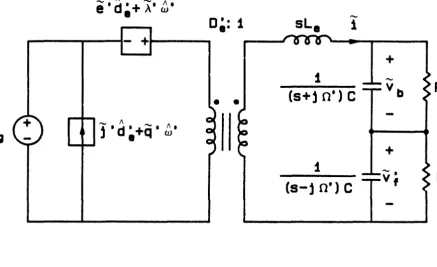
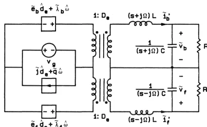
Since the rotating coordinates have been more versatile than the stationary ones in the two previous analyses, they are retained here to discuss the equivalent circuit. Again, ln the rotating frame of reference, an ideal converter is described by differential equations with constant coefficients. In particular, the complex ofb axes promise a single symmetrical model. instead of two unsymmetrical coupled circuits as the real dq axes. Therefore, the ofb coordinates are the most convenient common ground for later comparison of topologies in all four areas of power electronics.
To be "canonical", the model should identify correctly the output variable, input variable, conversion function, and filter topology. The output variable is usually the output voltage phaser, and the input variable the
source current phasor. The conversion function is the heart of the model:
"'
First, select the capacitor voltage phaser vb as the output and recall the linearized dynamic equation for this state:
(1.43)
Since no controlled generators are allowed at the output, the right-hand side of Eq. (1.43) is defined as an effective inductor current
'i'
=
n:
i+
1J,
~
-
1
cv
b &) 'so that
vb
now satisfies[
~
+
(s +j O')CJ
vb
( 1.44)
(1.45)
The above relation between
vb
and'i'
suggests that the impedance in squarebrackets is the first element of the model. as is shown in Fig. 1.4. Substitution of Eq. ( 1.44) into the linearized equation for
v
1 , the complex conjugate of Eq. ( 1.43), yields( 1.46)
Again, to push the controlled source by
CJ'
to the input side of the model requires the definition- . Vg RC2J'
=
v I - J D' e 1 +(s-jO')RC( 1.4 7)
Equation ( 1.46) then becomes
[
~ +(s-jO')C]v/
( 1.48)""'
""
The impedance in Eq. ( 1.48) relating
v
1 and 't thus becomes the second-
/\-
/\e'd;+A'w'
o;:
1
sL
8-
1
+
1
Cs+jn')C
vb
• •
-
/\ /\Vg
j 'd
~+q'
w'+
1
-
.
Cs-j n•)
c
v,
Fig. J. 4 Linearized, continuous, and time-invariant canonical model of the boost inverter.
From the previous steps. it is clear that the true inductor current i
and forward capacitor voltage
v
1 have to be sacrificed so that the physical outputvb
is preserved as the model output and all controlled generators are eliminated at the output half of the model. Therefore, care must be taken not to interpret model states, except for the output, as converter states. The true states can be retrieved from the model via Eqs. ( 1.44) and(1.47).
There still remains the linearized equation of the inductor:
(1.49)
'°" ... N
Replacement of i and v 1 in the above by i. and v 1 , respectively, and
R
'Y
manipulation of the resulting form to expose ,,, . v 1 , vb, and vg. give the following for the inductor in the model:
where
and
L
D'2 ,
e
.... , _ . lr V9 , .... s L8
l
t... -
-1
RC l+(s-jO')RC+De
vb R
( 1.50)
( 1.51a,b)
(1.51c)
Note that Eq. ( 1.50) automatically insures that the voltage source 'Ug in the
model represents truthfully the actual de supply, also vg. At this stage, no more new current or voltage states can be defined. Nonetheless. the last term in this equation may be treated as the secondary voltage of a
1 .
transformer whose turn ratio is the inversi.on ra.tio - , and whose primary
De
is fed by the source and dependent voltage generators inside the parentheses. The inductor, transformer, and voltage generators involved in Eq. (: .50) are illustrated in Fig. 1.4.
The one parameter that the procedure outlined above may not account for correctly is the source current. Actually, this current is irrelevant as long as the source is assumed to be ideal - this is why the modeling process ignores it completely in the first place. Nevertheless, the
From Fig. 1.4, the reflected current on the primary side of the
transformer is
't
.
I ,,.. ,DIi ,
=
't+
n'
Ii dejCV,,
-~- (j•
n'
Ii ( 1.52)Since the correct line current is only i, a controlled current generator must be inserted as shown in Fig. 1.4 to absorb the last two terms in the primary current. Thus,
....
,
J
n:
I and q ...,
""'
cv,,
-j
n:
( l .53a,b)The complete model thus characterizes faithfully both the output voltage and input current. It highlights the principal attributes of a power processor, namely, the control functions, conversion mechanism, and low-pass filters. Most importantly, it represents the nonlinear, switched, and time-varying converter by a linear, continuous, and time-invariant circuit.
PART I
CHAPrER 2
REVIEW OF EXISTING INVERTERS
Many industrial applications, such as motor drives and uninterruptible power supplies, require the conversion of de into ac power. This dc-to-ac power transformation is broadly called inversion, and the corresponding power processor the inverter. Although an inverter can have single-phase or balanced polyphase ac output, only the later type is considered in this thesis in accordance with the restriction of constant instantaneous power flow set forth in the Introduction. The terms "balanced
polyphase" thus describe a set of two or more sinusoidal quantities that have the same amplitude and are displaced in phase by ±90°, for a
two-360°
phase (or semi-four-phase) system, or ± M , for an M (~3)-phase system.
The "fast-switching" group. surveyed in Section 2.3. consists of inverters switched above two decades of the output frequency. Although most of these topologies suppress the switching ripple easily by small tilters. they are not genuinely balanced polyphase and. hence, generate nonlinear distortion as troublesome as the switching noise in the slow-switching family.
2.1 Inverters Switched at Low Frequency
This section deals with inverters whose switching frequency is of the
same order as, and often equal to, the output frequency. A great deal of operation fundamentals, harmonic analysis techniques, and design procedures for these inverters can be found in [6] and [26]. Recent advances in the inversion field on both theoretical and practical grounds have been edited in [7]. A survey of these and other documents in the literature suggests that the voltage-source, current-source. and, to a lesser extent, step-synthesis inverters are typical of the slow-switching category.
2.1.1 Voltage-Source Inverter
The voltage-source inverter [8] has been widely used as a variable-voltage, variable-frequency drive for ac machines. A three-phase topology simply consists of three double-throw switches permanently attached to the load, as is shown in Fig. 2.1 a. In a practical circuit, each throw is realized by a pair of anti-parallel thyristor and diode ; and the variable voltage source, a phase-controlled rectifier followed by an LC filter.
The three independent switching functions associated with the switches are sketched in Fig. 2 .1 b. Recall that according to the convention
•
a)
b)
c)
•
d11
1 ...
- - - 1 - - - + - - - - #2
- - - t i o - - - t+
v12-
3 ---'"'
•
d21:J
_____________
~~~~~..._
______ _
v12
~
v2s
L
I
r.-r
L
of the second pole (switch), which brings the second phase of the load to the positive end of the source. Although the switches are functionally independent. their timing must follow the six-stepped schedule in Fig. 2. lb and cannot be arbitrary because three-phase symmetry needs be preserved. The resulting line-to-line. or line. voltages are illustrated in Fig. 2.lc. The frequency of these voltages is controlled by the switching frequency as the
two are equal. Their amplitude, however, cannot be changed via the switches in the topology and. hence, must be adjusted via the de supply which, therefore, is either a phase-controlled rectifier or a chopper.
The voltage-source inverter has been famous for its simplicity in drive and control. It. however, generates a fair amount of harmonics that cause additional heating and torque pulsation in motor loads. The use of phase control to regulate the amplitude draws current harmonics from the main and degrades the input power factor, generally lagging. These drawbacks have led to the gradual substitution of the six-stepped by the PWM drive in medium-power applications.
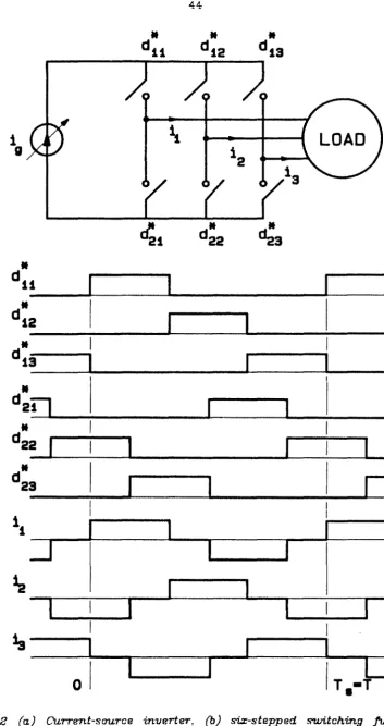
2.1.2 Current-Source Inverter
The current-source inverter [9] has gained considerable attention in the last several years. As is described in Fig. 2.2a, it consists of two triple-throw switches, instead of three double-triple-throw switches as in the voltage-source inverter, permanently attached to a variable current voltage-source. In a practical circuit, each throw is realized by a thyristor; and the current source, a phase-controlled rectifier in series with a large inductor.
Although they are topologically independent, the two switches must be synchronized as in Fig. 2.2b to ensure three-phase symmetry. Whenever a phase of the load is contacted by a throw, it receives a current identical in form to the switching function of that throw. Therefore, each net phase current is simply the scaled difference between the switching functions associated with that phase, as is illustrated in Fig. 2.2c. Control of the output frequency is exercised via the switching frequency because the two are identical; adjustment of the amplitude is provided by the de input.
a)
b)
c)
1
g
11
1c!
r=
~---~----~--~-ol
I
T •T
L
•
because of phase control. Besides the harmonic drawback, the current-source inverter requires a bulky and expensive 60 Hz inductor. The size of the inductor, in turn, results in a very sluggish drive with poor dynamic performance. The inductive current source also induces large voltage spikes across the switches if it is fed directly into an inductive load, such as an induction motor.
As the voltage-source inverter, the current-source inverter is an ideal topology capable of synthesizing very clean power if it is switched at sufficiently high frequency and driven by PWM, instead of six-stepped, waveforms. Surprisingly, although the PWM voltage-source inverter has been proposed for a long time, the dual PWM current-source inverter still has not been reported. The major difficulty probably lies in the correct identification of the switches: if the switches in Fig. 2.2a were mistakenly represented as three double-throw switches, used for voltage-fed inverters, instead of two triple-throw switches, used for current-fed inverters, the synthesis of a PWM strategy would be impossible. PWM techniques for voltage- and current- fed dc-to-ac converters are studied in the next chapter and applied to the topologies in Figs. 2.la and 2.2a to make them ideal.
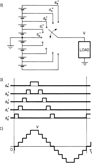
2.1.3 Step-Synthesis Inverter
The inverter is composed of a multiple-throw switch attached to the load, as. is seen in Fig. 2.3a. The throws connect the load to different voltage levels created by the bank of power supplies, realized by an autotransformer with the required amount of taps in practice [ 11]. In each cycle, the top five throws are activated according to the timing waveforms in Fig. 2.3b; the bottom four throws are controlled by functions 180° out-of-phase with those of the top four. The duty ratios are programmed to minimize the distortion in the "quantized" sine wave of Fig. 2.3c. Voltage control can be achieved through the source as in the previous two cases. Alternatively, two sinusoids like that in Fig. 2.3c can be synthesized and added to provide one output; their phases are then adjusted to vary the summed amplitude [ 12].
In principle, the quality of the output improves with a higher number of steps. This improvement, however, is at the expense of an excessive amount of switches and complex control circuitry. The step-synthesis inverter is thus justified only for high-power applications that require sinusoidal waveforms.
v
LOAD
b)
d*~ ____ ....__._ __ ._.._ ________________ ..,._
3
d; ... __ ... _.. ______
L-.1 _ _ _ _ _ _ _ _ _ _ _ _ _ _ _ _ . . . , _d; ... _.. ________ ...
'--111 _ _ _ _ _ _ _ _ _ _ _ _ _ _ . . . , _d* .... 1...11 _ _ _ _ _ _ _ _ _ _ _ _ . . . _ . _ _ _ _ _ _ _ _ _ _ _ _ _ _ _ _
0
c)
v
0
2.2 Inverters Switched at Medium Frequency
In the medium switching frequency range, "PWM inverter" refers generically to a voltage-source inverter (Fig. 2.1a) whose duty ratio varies from one switching cycle to the next. Even the switching frequency does not have to be constant. In 60
Hz
applications, for instance, the practical switching speed may be anywhere from 60Hz
to 1kHz,
the upper bound being imposed by the slow speed of high-power semiconductor devices and the heat loss at high switching frequency [13 and 14]. Because of this medium switching frequency, it is impractical to separate the switching noise from the desired frequency component unless bulky inductors and capacitors can be tolerated. Therefore, ever since the introduction of the "sinusoidal PWM" (also called "triangulation method" or "subharmonic control") [ 13], a variety of other PWM schemes have been born mainly to optimize the harmonic figure. These ramifications include the "multimode" [14], "optimal" [15], "selective-harmonic-elimination" [16], "current-controlled" [17], and so on PWM strategies. The sinusoidal PWM is deferred until the next chapter where it is studied in depth (although the switching frequency there is much higher, the basic principle is still the same). The other kinds of PWM are reviewed below.2.2.1 Multimode PD
the converter is highly sensitive to the pulse number and the synchronization between the carrier and modulation signals. Without any synchronization, the difference between the switching and inversion frequencies accumulates into a slow beat frequency that modulates the output waveform. The resulting beat power gives rise to the troublesome fluctuation in the steady-state torque and speed of ac machines. Even if the two frequencies are perfectly synchronized, the purity of a PWM spectrum deteriorates to that of a six-stepped spectrum as the modulation frequency approaches the carrier frequency. Under this circumstance, the six-stepped
drive is preferred to PWM drive because the former provides higher amplitude.
The multimode approach thus tries to select the best wav~form tor each range of amplitude and frequency. It starts at the sinusoidal PWM and gradually phases out all modulations until it reaches the six-stepped style. Needless to say, it demands a great deal of complicated circuitry to implement each mode, decide when to switch mode, and ensure smooth transitions.
2.2.2 Optimal PWlI
In the optimal PW M [ 15], the number and positions of the pulses or notches within each switching cycle are selected so that the corresponding spectrum optimizes some performance index of the system. The performance index can be any function that depends on the modulation policy; examples are the harmonic loss, torque pulsation, or load currents. In [15], the rms (root-mean-squared) value of current harmonics is chosen as the index and calculated as a function of the number of commutation pulses and the commutation angles. The proper placement of the commutation angles then minimizes the influence of harmonics on the load.
Since the functions involved are generally complicated and load-dependent, they can only be solved numerically. Thus, computation power from a microprocessor is needed to synthesize the correct switching
2.2.3 Selective-Harmonic-Elimination PWM:
Unlike the optimal PWM, the selective-harmonic-elimination technique [ 16] attacks the harmonics more directly by suppressing an arbitrary number of them in the output spectrum. The problem is formulated around a waveform that is chopped M times and possesses odd quarter-wave symmetry. Such a waveshape is characterized by M angles describing where the pulses start or end. Consequently, all harmonics can be computed in terms of these M pulse angles, and any M harmonics can be nullified by solution of the corresponding M simultaneous transcendental equations.
Closed-form solution of these equations, however, poses a formidable task, especially as the number of harmonics to be eliminated increases. Therefore. a computer is essential for numerical solution. If high performance is desired, a considerable amount of digital integrated circuits are involved to translate the mathematical results into the switching functions for the inverter.
2.2.4 Current-Controlled PWM
Instead of optimizing some performance index or eliminating some harmonics. the current-controlled PWM [17] cleans up the output currents directly by closed-loop regulation. In this scheme, the currents with
Three independent regulators are closed around the inverter in [ 1 7] to control three line currents; each has its own switching frequency related to its output. During some intervals, however, only two loops actually work while the third stays idle at zero switching frequency: the three loops are not all needed as the regulated quantities always sum up to zero (assuming no neutral-return path).
It is shown in the next chapters that at high switching frequency, the feedback problem can be formulated and solved differently. Describing equation can be used to predict the effects of energy-storage elements on closed-loop performance. The circuit implementation is much simpler since the principle requires only one regulator loop with one switching frequency.
2.3 Inverters Switched at High Frequency
This section consists of two parts. The first reviews the
switched-mode power amplifier. an earlier effort in PWM dc-to-polyphase conversion.
The second examines the resonant inverter, an example of energy inversion
with a resonance link.
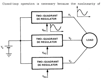
2.3.1 Switched-Mode Power Amplifier
As is illustrated in Fig. 2.4. a three-phase switched-mode power a:mplifier [ 19] is composed of three de regulators that amplify three-phase
reference signals into three-phase power for the load. Each block labeled
"Two-Quadrant De Regulator" actually consists of any de topology and a
feedback loop designed to match the output to the reference with very little
error. Closed-loop operation is necessary because the nonlinearity of de
TWO-QUADRANT V1
&
DC REGULATOR
TWO-QUADRANT V2
DC REGULATOR
vg
l
VR2TWO-QUADRANT V3
DC REGULATOR
Fig. 2. 4 Switched-mode amplifier with sinusoidal phase voltage ridi:ng on
power stages prevents sinusoidal outputs for open-loop sinusoidal duty ratio
modulation [20]. Note that the amplifier as a whole is four-quadrant even though each de block is current two-quadrant. Current bidirectionality is realized by two-quadrant-in-current switches in the individual topology; and voltage bidirectionality, the back-to-back arrangement of all three topologies.
If the loop is closed properly, the feedback complexity is compensated by clean output waveforms. The overall system is rugged in the presence of unbalanced load because the regulators essentially operate independently from each other. Since each block is quadrant, only two-quadrant switches are required. The switch simplicity, however, is at the expense of many power stages and reactive elements, a result of the simplistic conglomeration of many smaller units without taking advantage of the topological simplification offered by polyphase synergism. Additional circuitry is also needed in the feedback loops to correct the nonideality of the de topologies.
I