TECHNICAL REFERENCE MANUAL
Xerox Professional Computer
Reprint permission granted by Zilog, Inc. for Zilog Reprint on pages 49-108.
Reprint permission granted by Shugart Associates for SA 14030 Controller Reprint on pages 253-278.
Reprint permission granted by Western Digital for Western Digital Reprint on pages 279-302.
Zilog, Z80G!>, and Z80-A are trademarks of Zilog, Inc., with whom the publisher is not associated.
8086 is a trademark of Intel Corporation.
IBM,IBM PC, and IBM PCXT are trademarks of International Business Machines.
XeroxG!>,
820'·,820-11'·,
and 1618'· are trademarks of Xerox Corporation.CPIMG!>, CP/MG!>-80, and CP/M-86G!> are registered trademarks of Digital Research, Inc.. MS'· is a trademark of Microsoft Corporation.
WARNING: This equipment has been certified to comply with the limits for a Class B
computing device, pursuant to Subpart J of part 15 of FCC Rules. Only peripherals
(computer input/output devICes, terminals, printers, etc.) certified to comply with the Class B limits may be attached to this computer. Operating with non-certified peripherals IS likely to result in interference to radio and TV reception.
WARNING: This equipment generates and uses radio frequency energy and if not installed and used properly, that IS, in StrICt accordance with the manufacturer's instructions, may cause Interference to radio and television reception. It has been type tested and found to comply with the limits for a Class B computing device in accordance
with the specifications in Subpart J of part 15 of FCC Rules, which are designed to provide reasonable protection against such Interference in a residential installation. However, there is no guarantee that interference will not occur in a particular installation. If this equipment does cause Interference to radio or television reception, which can be determined by turning the equipment off and on, the user is encouraged to try to correct the Interference by one or more of the following measures:
Reorient the receiving antenna.
Relocate the com puter with respect to the receiver. Move the computer away from the receiver.
Plug the computer into a different outlet so that computer and receiver are on different branch CIrCUitS.
If necessary, the user should consult the dealer or an experienced radio/teleVision technician for additional suggestions. The user may find the following booklet prepared by the Federal Communications Commission helpful. This booklet is available from the U.s GOVERNMENT PRINTING OFFICE, WASHINGTON, D.C. 20402, STOCK NO. 004-000-00345-4.
"HOW TO IDENTIFY AND RESOLVE RADIO-TV PROBLEMS"
THIS PAGE
INTENTIONALLY BLANK.
Table of Contents
Introduction
Introduction
&
Miscellaneous Information
• Hardware Description
• Configurations and Product Codes
• Functional Description
• Hardware Interface
• Operating Systems:
CP/M-80
CP/M-86
MS-DOS
Hardware
Miscellaneous Hardware Information
• Dimensions
• Electrical Requirements
• Operating Environment
• Disk Drive Storage
• Disk Drive Format
• Display Specification, Functional Description,
and General Information
• System Bus Expansion Slot - Electrical
&
Environmental Requirements
• Hardware Interface - Connectors:
J 1 (Disk), J2 (Keyboard).
J3
(Pri nter), J4 (Comm)
J1 Illustration
J8 Illustration
J5, J6 (Power Supplies), J7 (Video Connector)
J8 (Parallel Connector)
Parallel Connector Illustration
J9 (COMM Port Strapping Options)
J9 (COMM Port Strapping Options) (Etch 2 CPU)
J 13 (System Bus)
J 12 (Disk Access)
J1 (Floppy Disk)
J 1 (Rigid Disk)
2
3,4
4,5·
5,6
6-9
9,10
10,11
13
13
13
14
14
15-17
18
Hardware
continued
Theory of Operation
• CPU
• ROM and RAM Memory
• 6 - 8k ROM Memory
• 64k RAM
• Counter Timer Circuit
• Serial
110 Controller
• Serial
liD Ports
• Parallel
liD Controller
• Parallel Port
• CRT Controller
• CRT RAM Memory Allocation
• Scroll Register
• Speaker
• Disk Drive Daughter Board
• Rigid Disk Drive Caution
• System Bus
• Keyboard Interface
Zilog Reprint (SID, Pia, CTC,
& CPU Data sheets)
Schematics:
vi
#1
Etch 1 CPU - Power Distribution
#2
Etch 1 CPU - CRT Controller
#3
Etch 1 CPU - CRT Controller
#4
Etch 1 CPU - U 16, U26, U28, U32, U37-U41, U54,
U57, U58
#5
Etch 1 CPU - U41, U54-U58, U66-U73
#6
Etch 1 CPU - RAM
#7
Etch 1 CPU - CTC
#8
Etch 1 CPU - GP, PIO,
510
#9
Etch 2 CPU - Power Distribution
# 1 0
Etch 2 CPU - CRT Controller
#11
Etch 2 CPU - CRT Controller
#12
Etch 2 CPU - U16, U26, U28, U32, U37-U41, U54,
U57, U58
# 13
Etch 2 CPU - U41, U54-U58, U66-U73
#14
Etch 2 CPU - RAM
# 15
Etch 2 CPU - CTC, Keyboard, PIO
#16
Etch 2 CPU - GP, PIO, SID
Hardware
continued
#17
Floppy Controller - Power Distribution
#lS
Floppy Controller
#19
Rigid Controller
#20
SOS6 Processor - Power Distribution
&
Connectors
#21
SOS6 Processor - U21-U24, U29-U32
#22
SOS6 Processor - U27, U33-U42
#23
SOS6 Processor - U l-U 16, U lS-U20, U25, U26, U28
#24
Memory Expansion PWB - 8086
Software
Device Initialization
• How the ROM works
Counter Ti mer Circuit
System PIO Controller
General Purpose PIO Controller
510 Controller
Channels A & B Baud Rate Generator
• Monitor Commands - Summary Table
Display Memory, Modify Memory
Xtended Memory, Fill Memory
Copy Memory, Verify Memory Block, Go To
Input, Output
Load From Disk
Read Disk Sector, Write Disk Sector
Baud Rate, Typewriter, Host Terminal Mode
Host Terminal Options
Host Terminal Command Set
Protocol
Operating System Interface
• Accessing BIOS
• Logical/Physical Device Mapping
• 1/0 Port Assignments
• ROM Operating System Interface
• CRT Entries
• Execute Physical Driver Entries
• Printer Entries
• Communications Entries
Software continued
• Keyboard Entries
• 10BYTE Directed I/O
• ,Programmable Functions
Sample Code Sequence
• Miscellaneous Functions - Cold, Warm, Getsel,
Daytim, Config, Start Screen Print
CRT Control & Interface
• Modes of Operation
• Text Character Set
• Graphics Character Set
• Display Manipulation
• Control Sequences
• Escape Sequences
Peripherals
Keyboards
• ASCII
• Low Profile (LPK)
Disk Drive Specifications
Disk Parameter Headers
Disk Formats
20
&
40
CPS Pri nters
• 20 CPS Operating Switches
• 20 CPS Command Codes
• 20 CPS Command/Control/Hex Code Chart
• 20 CPS Specifications
• 20 CPS Cabling Requirements
• 40 CPS - HPR05 Board
• 40 CPS Operating Switches
• 40 CPS Command Codes
• 40 CPS Command/Control/Hex Code Chart
• 40 CPS Electrical Interface
viii
166
167-169
170-176
177-179
177-182
183
184
185
186
186-188
189-193
195-199
200-206
207-212
213-218
219-226
,
Peripherals continued
",
• 40 CPS Specifications
251-252
• 40 CPS Cabling Requirements
252
SA1403D
Manual Reprint
253-278
Western Digital Reprint
279-302
Appendices
A.
BIOS
Entry Vector Table
A1-A6
B. Monitor Entry Vector Table
B1-B2
C. Documented System Storage & Structures
• Z80-A Mode 2 Interrupt Vectors
C1, C2
• Keyboard Interface
C1
• Logical to Physical Drive Mapping Table
C2
• Physical Driver Address Table & Request Block
C3
• Time-of-Day and Timer Variables
C4
D. Program Samples
• How to make Monitor Calls with BASIC
D1-D3
• Bank Program & Switching
D4
E. ROM Listings
E1-E 11 0
• CBIOS
E7-E 12
F.
Macros & Symbols
F1-F24
G.
Cold Start Loader
G1-G6
H. BIOS Jump Table
H1-H18
I.
Banked Physical Driver
11-112
J.
Position-Encoded Keyboard Handler
J1-J38
Appendices
continued
K.
Code Charts
• Baud Rates
• Decimal to ASCII to Hex
L.
Additional References
M. Contacts/reference:
• Diablo
• Digital Research
• Microsoft
• Shugart
N.
Abbreviations
x
Kl
K2
L1-L2
Ml-M2
Introduction
The purpose of this manual is to provide technical reference material for
the Xerox 820-11 and
16/8
Professional Computers for programmers and
engineers involved in hardware, software, and interface design. It is also
intended for interested persons who have a desire to know how the
Xerox 820-11 and
16/8
operate and how to access their many features.
A list of the abbreviations and naming conventions used in this manual
can be found in Appendix N.
SYSTEM OVERVIEW
Overview of Xerox Personal Computers
Xerox Personal Computers are comprised of four components:
display/processor, disk drives, keyboard, and optional printers. Both the
820-11 and 16/8 use the CP/M®-80 2.2 Operating System from Digital
Research, Inc. Additionally, the 16/8 PC includes CP/M-86® 1.1 and MS '"_
DOS Version 2.0 as standard operating systems.
HARDWARE DESCRIPTION
System Board
The system board uses a Zilog Z80-A®-based microprocessor operating on
a 4 megahertz clock with 64k RAM and 8k ROM. It is a single-board
computer and uses a daughter board to interface with the disk drives.
The 820-11 is equipped with three user-accessible I/O ports. Two of the
ports are located on the back of the display/processor; the third is
located on the CPU board. On the back are the printer and the
communications ports (both RS232C). The port inside the display is a
dual parallel port (most printers and other devices that follow a standard
Centronics 36-pin interface can be successfully attached).
The 16/8 has all of the above features as well as an InteI8086®-based
microprocessor operating with a 4.772 megahertz clock. The 8086 is
equipped with 128k of RAM which is expandable to 256k total by
adding a 128k daughter board to the 8086 board.
The 820-11 and 16/8 are capable of having up to 8k of read only memory
(four 2k ROMs): the 820-11 has 6k of this 8k occupied; the 16/8 uses the
full 8K. The last 2k on the 16/8 is used for decoding the position-encoded
Low Profile Keyboard. The firmware contained in the ROM is capable of
doing such things as executing a one-sector loader from disk; i.e.,
loading CP/M, emulating a terminal, operating in typewriter mode, etc.
The monitor also has other commands that are useful for debugging
hardware and software. The mother board also contains a speaker as
well as an expansion slot (used by the 16/8 for the 8086 board). There are
two types of daughter boards: one interfaces the display/processor to
floppy disks and the other interfaces the display/processor to a rigid disk
controller.
Display
The display/processor houses the video display, the CPU mother board,
the disk drive daughter board, and the 8086 processor board if so
configured. The video display is a standard 241ine by 80 characters. It
uses a 7 x 10 dot matrix for each character in all text modes and displays
white characters on a black screen. For graphics characters, it uses a 4 x 4
pixel resolution. The display attributes can be changed to display either
in blink, highlightllowlight, inverse, or graphics characters.
820-11 Display/processor for floppy disks
820-11 Display/processor for rigid disk
16/8 Display/processor for floppy disks
16/8 Display/processor for rigid disk
Keyboards
Product Code #U03
Product Code #UOS
Product Code #H69
Product Code #H70
The 820-11 and 16/8 use either a standard 96-character ASCII or Low
Profile keyboards. Both keyboards include additional keys to the right
of the keyboard, a 1 O-key numeric key pad and a set of keys for software
control of the cursor. The low profile keyboard also includes 12 function
keys that can be software-enabled and other keys such as Accept,
Delete, Next, Previous, Home, and Undo.
ASCII Keyboard
Low Profile Keyboard
Disk Drives
Product Code #X928
Product Code #G2S
Five disk drive options are offered for the 820-11:
Dual St" single-sided floppy disk drives
Product Code #X929
Dual St" double-sided floppy disk drives
Product Code #T66
Dual 8" single-sided floppy disk drives
Product Code #X973
Dual8" double-sided floppy disk drives
Product Code #F10
One 10mb rigid disk drive with
Product Code #U07
an 8" double-sided disk drive
Three disk drive options are offered for the 16/8:
Dual 8" single sided floppy disk drives
Product Code #X973
Dual8" double sided floppy disk drives
Product Code #F10
One 10mb rigid disk drive with
Product Code #U07
Printers
40 CPS Pri nter and 20 CPS Printer
As their names imply, the printers have a printing speed of 20 and 40
characters per second (CPS) respectfully. Both printers have a wide range
of print styles available. The 20 CPS Printer supports 10, 12, and 15 pitch
as well as Proportional Spacing (PS), while the 40 CPS Printer supports
either metal or plastic printwheels in 10, 12, 15, and P5. More detailed
information on these printers can be found in the Printer section under
Peripherals.
The standard R5232C printer connector and dual parallel port are
available to interface with many types of serial and parallel printers.
40 CPS Printer
20 CPS Printer
FUNCTIONAL DESCRIPTION
Product Code
#
080
Product Code
#
U01
The 820-11 and
16/8
systems are a collection of four components working
in unison -- the display, keyboard, disk drives, and printer. The
computer itself is housed in the display.
System Monitor -
ROM
The system monitor contained within the 8k ROM controls the essential
functions of initializing and controlling all system input/output
resources, and also provides a number of monitor commands that can
be used to assist in programming.
Ports
Three ports are standard on the 820-11 and 16/8: two serial ports located
at the back of the display unit and an additional dual parallel port inside
the display unit. These allow printers, communication devices, and
other peripheral equipment to be interfaced with the system.
Operating Systems
The 820-11 uses Digital Research's 2.2 CP/M-80 Operating System. The
16/8 can use Digital Research's 2.2 CP/M Operating System, as well as
their CP/M-86 1.1 Operating System and Microsoft's MS-DOS 2.0
Operating System. These operating systems provide the user with a
general environment for program construction, storage, and editing,
along with assembly and program checkout facilities.
CP/M-80 operating system software as implemented on the 820-11 and
the 16/8 is logically divided into four parts:
ROSR
BIOS
BDOS
CCP
ROM Operating System Routines (hardware dependent)
Basic
110
System (hardware dependent)*
Basic Disk Operating System*
Console Command Processor*
*Disk resident portions of CP/M-80
ROSR provides code in ROM that can be executed without the presence
of the CP/M system disk and provides the primitive operations necessary
to access the disk drives and to interface with peripherals.
BIOS provides the interface between BDOS and ROSR.
BDOS provides disk management by controlling one or more disk drives
containing independent file directories.
CCP provides symbolic interface between the user's console and the
remai nder of the CP/M system.
HARDWARE INTERFACE
The 820-11 and 16/8 are equipped with six input/output connectors. Four
are on the back of the display unit and two are inside the display.
Disk Drive
Used for connection of either the 8" or the 5{" Dual Floppy Drives, or
the 8" Rigid Disk Drive. This is determined by the type of disk daughter
board installed in the display processor.
Keyboard
Used for connection of either the ASCII or Low Profile keyboard.
Printer
A serial printer can be attached to this RS-232-C connector.
COMM
Parallel Port
A dual parallel port inside the display cabinet is also provided.
Expansion Slot
The expansion slot inside the display cabinet provides all of the ZSO-A
microprocessor control signals for connection to custom devices for
future expansion. This slot is used for the SOS6 co-processor if you have
a
16/S.
CP/M-SO
The CP/M-80 2.2-C disk for the 820-11 contains the standard Digital
Research software development and checkout programs. Xerox issues
additional utility programs that are unique to the 820-11. A description of
each program is listed below:
Digital Research Files
ASM.COM
The Assembler allows you to create a program
DDT.COM
DUMP.COM
ED.COM
LSO.COM
LOAD.COM
M80.COM
MOVCPM.COM
PIP.COM
STAT. COM
SUBMIT.COM
6
which can be read and executed by the S20-11.
The Dynamic Debugging Tool is used to debug a
ZSO-A assembly language program.
Allows binary command files that are not displayed
on screen to be displayed showing the hexadecimal
value for each byte.
A line-oriented screen editor.
Reads an .REL file created with the Macro-SO
Assembler Program and outputs a command file.
Reads a .HEX file and creates a command file.
Converts a program written in Assembly Language
to a relocatable (.REL) file and (optionally) a printer
listing file (.PRN).
Lets you modify and move the CP/M system image to
allocate a specific lesser memory size.
Allows you to selectively copy a file or files from one
disk to another or on the same disk.
The status utility is a frequently-used transient
command for all system housekeeping; i.e.,
checking the amount of space available on a disk.
Used to submit a file of commands for batch
processing.
SYSGEN.COM
XSUB.COM
Xerox Files
BACKUP. COM
CONFIGUR.COM
Used to generate a CP/M-80 system image and copy
the operating system to another disk.
Same as Submit.com, but has the facility to include
line input to programs as well as the console
command processor.
A multi-option utility that allows you to archive and
retrieve files, delete files, list directories of any
drive, and to verify data integrity of a floppy or rigid
disk.
Using Configur.com, you can select seven different
options:
1. Record Restart Command - lets you enter a
one-line command which will automatically load a
program. For example, you could enter DIR as
the restart command and every time you boot
the system, it will automatically display the
directory for you. Or you could enter the name
of your application software package and it
would automatically load that application
package for you. This command is recorded on
the disk and you can have a different one for
each disk.
2. Select Printer Port Options - allows you to
determine printer protocol. This option allows
configuration for alternate printers without
modifying the BIOS.
3. Select Communications Port Options - a
convenient method for setting up the
communications port on the 820-11 or 16/8; that
is, baud rate, protocol, stop bits, etc.
4. Select I/O Device Assignments - lets you select
alternative input/output device assignments;
i.e., set up the system so that everything
displayed on the screen automatically prints on
the pri nter.
5. Select Keyboard Data Format - lets you choose
7-bit or 8-bit mode for the keyboard.
COPY.COM
FMT.COM
HELP.COM
INIT.COM
KILLESC.COM
SET.COM
SWAP.COM
TlME.COM
WHATSA.COM
8
7. If you have a floppy disk system, Select Floppy
Disk Head Step Rate will appear as selection 7. If
you have a rigid disk system, Configure Rigid
Disk will appear (program must be loaded from
floppy or the first partition of the rigid).
a.
Select Floppy Disk Head Step Rate - lets you
adjust the floppy head step rate for
optimum performance.
b.
Configure Rigid Disk - lets you divide the
eight megabyte rigid disk into sections
(e.g., 4 Mb, 2 Mb, 1 Mb, 1 Mb).
Makes an exact copy of a disk, track for track.
Allows you to format (initialize) a rigid disk.
Verification of the rigid disk is performed using the
Backup.com utility.
A guide for CP/M-80 users that contains basic
information about CP/M-80 commands; also
cross-references to additional information in the CP/M-80
reference manual, Reorder #9R80448.
Prepares new (or used) disks for storing
information. It will also alert the user to any flawed
sectors on the disk.
Turns off the <CTRL>
+
<ESC> feature to enable
use of <CTRL>
+
<ESC> for other purposes; for
example, setting margins and tabs on a 40 CPS
printer uses a <CTRL>
+
< ESC> sequence.
A convenient method to temporarily change
communication and printer port options in RAM.
A utility that allows the user to swap drive names.
For example, "A" and "E" for a rigid disk drive. By
designating an alternate drive as the" A
Rdrive, you
can load software directly from that drive. Many
CP/M-80 application packages have been written to
be executed from the
RAH disk drive only. Using
Swap.com allows you to place your application
software on any disk drive and load.
Displays the time and date on screen. Since there is
no battery backup, however, you must re-enter the
time and date each time you reload the system.
This utility lists the logical and physical names for
each disk drive, as well as the density, number of
sides, and types of disks logged into the system,
(e.g., double density, single-sided S" floppy).
CP/M-86
The CP/M-SO 2.2 and CP/M-S6 1.1-F disks for the 16/S contain the
standard Digital Research software development and checkout
programs. These disks contain the same files as described in the CP/M-SO
section as well as the following files.
Digital Research Files
ASMS6.CMD
The Assembler allows you to create a program
DDT86 .. CMD
ED.CMD
GENCMD.CMD
GENCMDCOM
GENDEF.CMD
GENDEF.COM
HELP.CMD
LMCMD.CMD
LMCMD.COM
PIP.CMD
which can be read and executed by the SOS6.
The Dynamic Debugging Tool is used to debug a
SOS6 assembly language program.
A line-oriented screen editor.
Uses the hex output of ASM-86 and other language
processors to produce a .CMD file.
Uses the hex output of ASM-86 and other language
processors to produce a .COM file.
Reads a 16-bit file containing the disk definition
statements, and produces a 16-bit output file
containing assembly language statements which
define the tables necessary to support a particular
drive configuration.
Reads a 16-bit file containing the disk definition
statements, and produces an 8-bit output file
containing assembly language statements which
define the tables necessary to support a particular
drive configuration.
Provides summarized information for all of the
CP/M-S6 commands described in the Digital
Research Users manual.
Operates in exactly the same manner as
Gencmd.cmd, except Lmcmd also accepts an Intel
L-module file as input.
Operates in exactly the same manner as
Gencmd.com except Lmcmd also accepts an Intel
L-module file as input.
STAT.CMD
SUBMIT.CMD
TOD.CMD
Xerox Files
CPM86.COM
86CON.COM
GOBACK.CMD
LOAD86.COM
REBOOT.COM
SOFTKEYS.COM
The status utility is a frequently-used transient
command for all system housekeeping, i.e.,
checking the amount of space available on a disk.
Used to submit a file of commands for batch
processing.
Time of day.
Used by Load86.com to boot the 8086.
Switches from Z80-A console to the 8086 console.
Switches from 8086 console to the Z80-A console.
Loads the 8086 for concurrent processing.
From the concurrent mode, reboots the system as a
Z80-A standalone.
Used to set up the 10-key pad with programmable
functions
«
CTRL> + one of the 1 O-key pad keys).
MS-DOS
The MS-DOS 2.0 disk for the
16/8
contains the standard Microsoft
software development and checkout programs.
Microsoft Files
ANSI.SYS
COMMAND.COM
CONFIG.SYS
CHKDSK.COM
CREF.EXE
DEBUG.COM
DISKCOPY.COM
EDLlN.COM
EXE2BIN.EXE
FC.EXE
FIND.EXE
FORMAT.COM
L1NK.EXE
MORE.COM
10
Allows programs that use the standard ANSI driver
to be executed.
This is the MS-DOS command processor. It is
recommended that this file be placed on every
application program disk.
Configures system at boot.
Checks disk.
Assists in debugging assembly language programs.
Debugger supplied with MS-DOS.
Copies a disk.
Line-oriented screen editor.
Converts .EXE files to binary format.
Compares two files for similarity.
Findsa string in a list of files or standard input.
Formats an 8" floppy or a rigid disk.
Linker.
Used to display text in 23-line segments.
MASM.EXE
PRINT.COM
RDCPM.COM
RECOVER.COM
SORT.EXE
Xerox Files
SAMPLE.TXT
Macro Assembler for MS-DOS.
Print spooler.
Reads a CP/M-80 file and converts data to
MS-DOS-readable file.
Recovers bad or damaged disks.
Used to sort text.
Notes
Specifications
This section details the following specifications: dimensions, electrical
requirements, operating environment, and disk drive capacities of the
Xerox 820-11 and 16/8 PCs.
Dimensions
Equipment
Height
Depth
Width
Weight
820-11-16/8 Display
12.20"
14.75"
15.00"
301bs.
ASCII keyboard
3.75"
9.50"
20.00"
101bs.
Low profile keyboard
1.60"
8.25"
19.90"
5lbs.
5t" Floppy disk drives
7.00"
10.20"
7.00"
101bs.
8" Floppy disk drives
10.50"
17.50"
14.50"
481bs.
8" Rigid disk drive
10.50"
17.50"
15.50"
541bs.
40 CPS pri nter
10.00"
17.50"
15.50"
561bs.
20 CPS printer
9.25"
17.50"
24.00"
451bs.
Electrical Requirements
All Xerox products listed below require voltage of 115 VAC, a frequency
of 60 Hz, and a two-pole, three-wire grounded duplex receptical.
Equipment
820-11-16/8 Display
8" Floppy disk drives
8" Rigid disk drive
40 CPS printer
20 CPS printer
Operating Environment
Current
1.1 Amps
2.0Amps
2.2 Amps
2.0 Amps
1.0Amp
Disk Drive Storage
5i"
Ss/sD
5rSS/DD
5i"
DSISD
5i" DS/DD
8" SS/SD
8" SSIDD
8"Ds/sD
8" DS/DD
8" Rigid (DS/DD)
Disk Drive Format
Equipment
5i" SS/SD
5i"
SSlDD*
Si"
DSISD
5t" DS/DD*
8" SS/SS
8" SS/DD**
8" DSISD
8" DS/DD**
8" Rigid DS/DD
Unformatted
Tracks
40
40
80
80
77
77
154
154
1,024
125 k
250k
250k
500k
400k
800k
800k
1.6Mb
10.67Mb
Sectors
18
17
18
17
26
26
26
26
32
Formatted
Usable
90k
81 k
168 k
155 k
180k
172k
338k
322 k
250k
241 k
497k
482k
500k
490 k
997 k
980k
8.4Mb
8.192Mb
Bytes
per
Number
of
Sector
128
256
128
256
128
256
128
256
256
Heads
1
1
2
2
1
1
2
2
4
*Track 0 of 5t" double density disks has 18 sectors of 128 bytes.
**Track 0 of 8" double density disks has 26 sectors of 128 bytes.
For more specific information on disk formats, see the Disk Drive
Specifications section.
DISPLAY SPECIFICATION
SIZE:
TYPE:
RESOLUTION:
CHARACTER CELL:
BUSINESS GRAPHICS:
CHARACTER SET:
CHARACTER LINES:
CHARACTERS/LINE:
VOLTAGE:
RIPPLE:
VIDEO BIT RATE:
BITS/HORZ LINE:
HORZ SYNC PULSE:
TOTAL BITS/LINE:
HORZ RATE:
LINES/FIELD:
VERT BLANKING LINES:
VERT SYNC PU LSE:
VERT RETRACE (lines):
TOTAL LINES/FIELD:
FIELD RATE:
REFRESH RATE:
VIDEO RATE:
12 inch,landscape mode
Aluminized
P4
Fluorescence
White (W)
Phosphorescence White (W)
Persistence
Short
• 240 active line raster adjusted to 8.5 x S.3
inch usable area
• Brightness level 30 (± 2) foot-Iamberts
• Resolution at centers (within 1" diameter
circle) -100 lines/inch minimum
7x10
4x4 Pixel Resolution
4 sets of 128:
(1 U.S. font, 1 Graphics
font) (1 U.S. font, Inverse
Video font)
24
80
+
12 (± 5.0%) VDCat2.0A DC maximum
50 MV
pop
synchronous or nonsynchronous
with refresh or power frequency.
10.694 MBPS
(93.51 nanoseconds)
560
126
(11.78 microseconds)
686
15.59 KHz
(64.14 microseconds)
240
20
20(1.28 milliseconds)
8TYP
260
59.95 Hz
(16.68 milliseconds)
FUNCTIONAL DESCRIPTION, XEROX DISPLAY
The display has the following functional characteristics:
•
24 line display
•
80 characters per line
•
7x10 dot matrix per character
•
White characters on black
•
Software-selectible character attributes
Inverse Video
Blink
Low Intensity
Graphics with 4 x 4 pixel resolution
•
Brightness adjust
DISPLA Y CONTROLLER
The Display Controller is based on displaying characters within a 7x10 cell
(7 dots horizontally by 10 scan lines vertically). To guarantee spaces
between characters, one dot on each side of the cell is blanked by
hardware. Also, to guarantee spaces between character lines, the top
two scan lines are blanked by hardware. This gives an actual active
character size of 5 dots horizontally by 8 scan lines vertically.
For Business Graphics, the hardware is configured to eliminate the
automatic blanking and allow continuous lines both horizontally and
vertically. However, the Display Controller is still based on displaying a
character within a 7 xl 0 cell. The controller design and available refresh
memory allows one byte per character. The maximum number of unique
characters that can be defined by any 8 bits is 256. Since the standard
text font set contains 128 characters, the limit on unique characters for
graphics that can be displayed together with text is 128.
The character set for Business Graphics divides the cell into blocks of 4
dots horizontally by 4 scan lines vertically. Since the total number of scan
lines per character is 10, the character set actually consists of two sub-sets
of 4-4-2 and 2-4-4.
Each subset divides the cell into 6 parts requiring 64 possible
combinations or unique characters. Therefore, the total number of
unique characters for the complete graphics set is 128. With this
character set, any combination of adjacent 4 x 4 blocks can be chosen.
Also, at the character cell boundary, the 4 x 4 blocks can be set vertically
by 2 scan lines. Since the total number of horizontal dots per cell is 7,
there will be an overlap of one horizontal dot in the center of the cell for
diagonal blocks within the cell.
SYSTEM BUS EXPANSION SLOT
ELECTRICAL
The
DC
system power available at the expansion slot is as follows:
PIN
50
PIN 45
+5VDC
+ 12V DC #1
5t"
system
1.2A
0.3A
8" or Rigid system
2.1 A
1.75A
ENVIRONMENTAL
The following temperature, humidity and altitude environmental
requirements are specified:
Operating
Non-operati ng
Temp.
(OCelsius)
10 to 32
-77
to
66
Rel.Hum.
(%)
20t080
15
to
90
Altitude
(miles)
1830
7620
Any optional or additional electronic assembly using the expansion slot
must be capable of performing to design specification when the host is
subjected to the environmental range, above. Furthermore, the
presence of such an assembly in the expansion slot must not degrade
performance with regard to the above environmental requirements.
MONITOR
~'
T I
T
..!..
HARDWARE INTERFACE
'r
MAIN PWA'~ Il~~GINDII!~~~
T
=±I
~
:
fRANDA!A
+
..l..!:ETEN..!..
±~
+
~
I':' VERT DR
'71
: HQflZ DR :
1
: VIDEO:
l
I I
I I
I I
I I
I I
I :
I I
I I
I I
+
20 DATA TERMINAL READY: 20I I
KEYBOARD
~, ::c:~: i
.0,
'2
"
:
.J.. 13 I
.J.. 14 :
±g
.L.
±
~O
.Ls
±:
.L.
.L.
+~
I 2 7 -'- 28
PM
pB1
OU
OM
pBS
DBI
DB?NSTROB
,-'-M~ I :
1
'::1
i
i :
±:
I:'III~~:
_~gy@i
':
~
±
~
GARRIER DETECTI
I I
I
I
9 T I I
22 - I TRAN SIG EL TIMING: 15
I t : :
REC S" EbT'MINGi
'7~ DATA TERMINAL READYI 20
SERIAL PRINTER
J1 illustration
20
PI Jl
IW WITCH 112 •
SEEK COM L 1 : + o SIDED : 1~+ lilT'
1 ,3 •
1'41
,'5
1HEAD E O. 1'71
lSi"
I DEX , ' 9 .
1 20 ,
READY t 21,
I ~;:r:
DAIV El 1 I 26+
1 27 •
1 28i"
DAIV L 129!
1 30T" DIVE EL4:;~~
EL ,33T ,34.
,35,
,36T WR e DATA I ~:I
: 39
r-,40,
1 41 , ,421
T1 43 • DATA
:iE
'471.
TOSA10Q4DRIV£@LV
JlO DAISY CHAIN
CONNfCTOR
TW IDEO: ~1+
~mm:=*125.L.
r-
7+
126~
HEAD LOAD I a
+
INO X I ~2:r:
as.!..
R ADY :
17t-, 17t-,
,5.
~
iD:' ~E:gf:
EL3 124123i-1 6 (
, ,
EL
:~+
STEP 1 28,lOr
r
WRITE DATA I ~r:130.!..
WRITE TE:
12f-TRACK 0 : -~~F W ITEP E T 32 ,
,'4,
I ~~r.J8 illustration
820·11
PARALLELJ8 P8 PRINTER
-30 PB2 PAD DATA STROBE 1
DATA BIT 0
- 6 l5ii 1 DATA BIT 1 2
-- 8 I5A2
DATA BIT 2 3
--10
PA3 DATA BIT 3 4
--12
PA4 DATA BIT 4 5
--14 PA5 DATA BIT 5 6
--16
"'A6 DATA BIT 6 7
--18 !Sii7
ISATA BIT 7 8
--20 PB7 ACKN~WLEDGE 9
--40
PB4 BUSY 1 0
--34
PB6 ON LINE
11--38 !S~O AUTO LF 1 3
--26 GND.
14--37
GND. 1 6
-- 1 " GND. 1 9
-- 5
GND.
20-- 7 GND.
21-- 9
GND.
22--11
GND. 2 3
--13
GND.
24--15
GND.
25-- 1 7
GND.
26--19
GND.
27--21"
GND.
28-- 3
GND.
29--35 GND.
30--39
GND.
36-22
POWER SUPPLY
Power Supplies. and Video Connectors
MAIN PWA
P5 J5
-12VDC , 1"'j'"
+ 12VDC CPU: 2+ +12VDC DIS I 3.l.
DCRET ;4+
DC RET • 5..1.. DC RET: 6+ + 12VDC CR I 7+
+5VDC aJ.. +5VOC 91.
MDNITOf! PW> Jl Pl
j7T
" '
;==='iIT
;::::=:::>':
I'1°
r
,BRIGHTNESS ' . : CONTROL I I
, I
Jl Pl : ~
8 '-,-,',
I 2.L--.!.. 3":'"' I I I 3-'_'4..!...
Parallel Port Connector (J8)
39
00000000000000000000
00000000000000000000
40
2
J8
Pin
Value
2
Port A Strobe
4
PortA Ready
6
PortA Bit 0
8
PortA Bit 1
10
PortA Bit 2
12
PortA Bit 3
14
PortA Bit 4
16
PortA Bit
5
18
PortA Bit 6
20
PortA Bit
7
22
Port BReady
24
Port B Strobe
26
Port B Bit 0
28
Port B Bit 1
30
Port B Bit 2
32
Port B Bit 3
34
Port B Bit4
36
Port B Bit
5
38
Port B Bit 6
40
Port B Bit
7
Parallel connector picture
GROlA'I> WIRE
24
/ ' J8 PRINTER PORT
INSIDE 820
FIRST PLUG
(not used)
PLUG
COMM Port Strapping Options
39
00000000000000000000
00000000000000000000
40
Pin
5--6
7--8
9--10
11--12
13--14
15--16
17--18
19--20
21--22
23··24
25--26
27··28
29--30
31··32
33--34
35··36
37--38
39--40
J9
Value
(M) TXD to Pin
3
(T) TXD to Pin 2
(M) RXD from Pin
2
(T) RXD from Pin
3
(M) RTS to Pin
5
(T) RTS to Pin
4
(M) CTS from Pin
4
(T) CTS from Pin
5
(M) DTR to Pin
8
(T)
DTR to Pin 20
(M) DCD from Pin
20
(T) DCD from Pi n
8
2
Clock supplied to Modem as RX Clock
Clock supplied to
510
with RX Clock
Modem supplies
510
with RX Clock
Clock supplied to
510
with TX Clock
Modem supplies
510
with TX Clock
Clock supplied to Modem with TX Clock
The filled-in pins indicate the options as they are jumpered on an 820-11
or 16/8.
29
30
J9
(Etch 2 CPU)
000000000000000
000000000000000
Pin
3--4
5--6
7··8
(M) TXD to Pin 3
(T) TXD to Pin 2
(M) RXD from Pin 2
(T)
RXD from Pin 3
(M) RTS to Pin 5
(T)
RTS to Pin 4
(M) CTS from Pin 4
(T) CTS from Pin 5
(M) DTR to Pin 8
(T) DTR to Pin 20
(M) DCD from Pin 20
(T) DCD from Pin 8
2
9--10
11··12
13--14
15··16
17--18
19··20
21--22
23··24
25--26
27··28
29--30
Clock supplied to Modem as RX Clock
The filled-in pins indicate the options as they are jumpered on an 820-11
or 16/8.
Note: To change from ASYNC to SYNC on the Etch 2 CPU requires a
modification to the operating system rather than moving jumpers.
Note:
26
(M) indicates modem (data communications equipment)
function. (T) indicates terminal data equipment) function.
For instance, exercising the (M) strap option will allow
communication with a modem; exercising the (T) strap
option will allow communication with a terminal.
The above shows factory settings for (T).
System Bus Connector
J13
Dl
1
2
IRD
DO
3
4
IMEMRQ
D7
S
6
IIORQ
D2
7
8
IWR
D6
9
10
IREFRESH
D5
11
12
IMl
D3
13
14
AD
D4
15
16
Al
SYSRESET
17
18
A2
A4
19
20
A3
A6
21
22
AS
A15
23
24
A7
A13
25
26
A14
A12
27
28
Al0
A9
29
30
All
A8
31
32
IBUSRQ
WAITRQ
33
34
IBUSAK
PC!
35
36
IINTRQ
37
38
IHALT
39
40
ICLOCK
SPKR
41
42
IMEM8
43
44
IMEM4
+12V
45
46
+12V
47
48
GND
Pin
Pin
Symbol
t!..
Name
Meaning
DO
3
Data bus
Data Bus (Tri-state, input/output,
Dl
1
Data bus
active high) constitutes an 8-bit
D2
7
Data bus
bi-directional data exchange
D3
13
Data bus
with memory and I/O devices.
D4
15
Data bus
D5
11
Data bus
D6
9
Data bus
D7
5
Data bus
AO
14
Address bus
Address Bus (Tri-state, output,
Al
16
Address bus
active high) makes up a 16-bit
A2
18
Address bus
address for up to 65k bytes of
A3
20
Address bus
memory for
1/0
devices data
A4
19
Address bus
exchange. I/O addressing uses
AS
22
Address bus
the lower 8 bits for direct
A6
21
Address bus
selection of up to 256 output
A7
24
Address bus
ports. AO is the least significant
A8
31
Address bus
address bit. During refresh time,
A9
29
Address bus
the lower 7 bits contain a valid
Al0
28
Address bus
refresh address for dynamic
All
30
Address bus
memories.
A12
27
Address bus
A13
25
Address bus
A14
26
Address bus
A15
23
Address bus
IWR
8
Write
Write (Tri-state, output, active
low) indicates that the CPU data
bus holds valid data to be stored
in the addressed memory or
1/0
device.
IRD
2
Read
Read (Tri-state, output, active
high) indicates that the CPU
wants to read data from memory
or an
1/0
device. The addressed
1/0
device or memory should use
this signal to gate data onto the
CPU data bus.
IIORQ
6
1/0
Request
Input/Output Request (Tri-state,
output, active low) signal
indicates that the lower half of
IHALT
39
IMEMRO
4
IRE FRESH
10
IM1
12
Halt
Memory
Request
Refresh
Machine
Cycle One
the address bus holds a valid
1/0
address for an
1/0
read or write
operation. This signal is also
generated with a
"/M1"
signal
when an interrupt is being
acknowledged to indicate that an
interrupt response vector can be
placed on the data bus. Interrupt
Acknowledge operations occur
during
"1M
1" time, while
1/0
operations never 6ccur during
"/M1"
time.
Halt (Output, active low) signal
indicates that the CPU has
executed a Halt Software
instruction and is awaiting either
a non-maskable or maskable
interrupt before operation can
resume.
Memory Request (Tri-state,
output, active low) signal
indicates that the address bus
holds a valid address for a
memory read or memory write
operation.
Refresh (Tri-state, output, active
low) indicates that the lower 7
bits of the address contain a
refresh address for dynamic
memories and the "/MEMRO"
signal should be used to perform
a refresh cycle for all dynamic
RAMs in the system. During the
refresh cycle" AT' is a logic zero
and the upper 8 bits of the
address bus contain the "I"
register.
that during the execution of
two-byte op-codes,
"1M
1 " wi II be
generated as each op-code is
fetched. These two-byte
op-codes always begin with a CB, DO,
ED, or FD.
"/M1"
also occurs with
"/IORQ" to indicate an interrupt
acknowledge cycle.
IBUSAK
34
Bus
Bus Acknowledge (Output,
Acknowledge
active low) is used to indicate to
the requesting device that the
CPU address bus, data bus, and
control bus signals have been set
to their high impedance states
and the external device can now
control the bus.
IBUSRQ
32
Bus Request
Bus Request (Input, active low)
signal is used to request the CPU
address bus, data bus, and control
signal bus to go to a high
impedance state so that other
devices can control those buses.
When "/BUSRQ" is activated, the
CPU will set these buses to a high
impedance state as soon as the
current CPU machine cycle is
finished and the "/BUSAK" signal
is activated.
IINTRQ
37
Interrupt
Interrupt Request (Input,
Request
active low) signal is generated by
1/0
devices. A request will be
honored at the end of the current
instruction if the internal
software controlled interrupt
enable flip flop (IFF) is enabled
and if the "/BUSRQ" signal is not
active.
IWAITRQ
33
Wait Request
Wait Request (Input, active low)
indicates to the CPU that the
addressed memory or
1/0
device is
not ready for a data transfer. The
CPU continues to enter wait states
for as long as this signal is active.
This signal allows memory or I/O
devices of any speed to be
synchronized to the CPU. Use of
this signal postpones refresh as
long as it is held active.
ISYSREST
17
System Reset
System Reset (Output, active low)
indicates that a reset has been
generated either from push
button reset or the power on
reset circuit. The system reset will
occur only once per reset and will
be approximately 10
microseconds in duration.
ICLOCK
40
Processor
Processor Clock (Output, active
Clock
low) is a single-phase system clock
of4 MHz.
PCI
35
Priority
Priority Chain In (Input, active
Chain In
high) is used to form a
priority-interrupt daisy chain when more
than one interrupt-driven device
is being used. A high level on this
pin indicates that no other
devices of higher priority are
being serviced by a CPU interrupt
service routine.
IMEM4
44
Memory
Memory Expansion
Expansion
(Output, active low) signal is low
during "/MEMRQ" for a block of
addresses from "4000 thru 7FFF"
if the Bank Switch is set for the
ROM side of memory.
IMEM8
42
Memory
Memory Expansion
Expansion
(Output, active low) signal is low
during "/MEMRQ" for a block of
addresses from "8000 thru BFFF"
if the Bank Switch is set for the
ROM side of memory.
+5VDC
50
GND
49,48
+ 12VDC 47,45
36
38
43
46
32
DC Power
Ground
DC Power
Not Used
Not Used
Not Used
Not Used
driver (75451). This output is
normally connected thru the
speaker and parallel 100 ohm
resistor to a + 12 VDC, but can be
disconnected by jumper option.
+ 5VDC system power.
Ground-System is signal ground
and DC return.
+ 12VDC system power.
Disk Access Connector
J12
01
1
2
IRO
00
3
4
IMREQ
07
5
6
IIORQ
02
7
8
IWR
06
9
10
IBU5AK
05
11
12
IMl
03
13
14
AO
04
15
16
Al
RST
17
18
A2
A4
19
20
A3
A6
21
22
AS
A15
23
24
A7
A13
25
26
A14
A12
27
28
Al0
A9
29
30
All
A8
31
32
IBUSRQ
16 MHz Clock
33
34
IBUSAKl
IHALT
35
36
11797CS
INT
37
38
PRIO
PP5
39
40
4MHz Clock
PP2
41
42
PP4
PPl
43
44
PPO
+12V
45
46
NMl
GNO
47
48
GNO
OSKWAT
49
50
+5V
51
52
+ 5V
J 1-19
53
54
J 1-1 0
J 1-18
55
56
J 1-9
J 1-17
57
58
Jl-8
J 1-16
59
60
Jl-2
J 1-15
61
62
Jl-3
J 1-14
63
64
Jl-4
J 1-13
65
66
Jl-5
J 1-12
67
68
Jl-6
J 1-11
69
70
Jl-7
Pin
Pin
Svmbol
It
Name
Meaning
DO
3
Data bus
Data Bus (Tri-state, input/output,
01
1
Data bus
active high) constitutes an 8-bit
02
7
Data bus
bi-directional data exchange with
03
13
Data bus
memory and I/O devices.
04
15
Data bus
05
11
Data bus
06
9
Data bus
07
5
Data bus
AO
14
Address Bus
Address bus AO-A 15
Al
16
Address Bus
provides addresses for 65k
A2
18
Address Bus
bytes of memory. Bit AO and
A3
20
Address Bus
A 1 while under fRO and IWR
A4
19
Address Bus
control select the register
AS
22
Address Bus
to receive transfer of data
A6
21
Address Bus
on 00-07:
A7
24
Address Bus
Al AO
fRO
IWR
A8
31
Address Bus
0
o
Status REG Command REG
A9
29
Address Bus
0
1 Track REG
Track REG
2Al0
8
Address Bus
1
o
Sector REG
Sector REG
All
30
Address Bus
1
1 Data REG
Data REG
2A12
7
Address Bus
AS while under fRO and IWR
A13
25
Address Bus
Control Select Density:
A14
26
Address Bus
o
=
double density
A15
23
Address Bus
1
=
single density
PPO
44
SYS-PIO PortA PortA bit 0
PPl
43
SYS-PIO Port A
PortA bit 1
PP2
41
SYS-PIO Port A
PortA bit 2
PP4
42
SYS-PIO Port A
PortA bit 4
PP5
39
SYS-PIO Port A
PortA bit 5
PRIO
38
SYS-PIO
fDSKWAT
49
Disk Wait
Generates Wait signal to CPU.
fRO
2
Read
Controls input on the data
registers 00-07.
fMREQ
4
Memory
fMREQ indicates that the address
Request
bus holds a valid address for a
memory read or memory write
operation.
IIORQ
6
1/0
Request
IIORQ indicates that the lower
half of the address bus holds a
valid
1/0
address for an
1/0
read or
write operation. IIORQ is also
generated concurrently with
1M
1
during an interrupt acknowledge
cycle to indicate that an interrupt
response vector can be placed on
the data bus.
IWR
8
Write
Controls output on the data
registers 00-07.
IBUSACK
10
Bus
IBUSACk indicates to the
Acknowledge
requesting device that the CPU
address bus, data bus, and control
signals IMREQ, 1I0RQ,
IRD,
IWR
have entered the high impedance
states. The external circuitry can
now control these lines.
IM1
12
Machine
1M
1, together with
1M
REQ
Cycle 1
indicates that the current
machine cycle is the op-code fetch
cycle of an instruction execution.
1M
1, together with 1I0RQ,
indicates an interrupt
acknowledge cycle.
IBUSREQ
32
Bus Request
IBUSREQ has the highest priority
and is always recognized at the
end ofthe current machine cycle.
IBUSREQ forces the CPU address
bus, data bus, and control signals
IMREQ, 1I0RQ,
IRD,
and IWR to
go to a high impedance state so
that other devices can control
these lines.
IBUSAK1
34
Bus
IBUSAK 1 is daisy-chained Bus
external circuitry can now control
these lines.
11797C5
36
Chip5elect
11797C5 logic low selects the
Floppy Disk Controller chip and
enables computer communication
with the device.
INT
37
Interrupt
INT is generated by
1/0
devices.
Request
The CPU honors a request at the
end of the current instruction if
the internal software controlled
interrupt enable flip-flop (IFF) is
enabled.
NMI
46
Non-Maskable NMI is always recognized at the
Interrupt
end of the current instruction,
independent of the status of the
interrupt enable flip-flop and
automatically forces the CPU to
restart at location 0066h.
IHAlT
35
Halt
IHAlT indicates that the CPU has
executed a Halt instruction and is
awaiting either a non-maskable
or a maskable interrupt (with the
mask enabled) before operation
can resume. While halted, the
CPU executes NOPs to maintain
memory refresh.
16MHz
33
Clock
16 MHz clock.
ClK
40
Clock
4 MHz clock.
Jl-2
60
Device I/O
All interface lines use
Interface
negative logic.
Jl-3
62
Device
1/0
Interface
Jl-4
64
Device
1/0
Interface
Jl-5
66
Device
1/0
Interface
Jl-6
68
Device I/O Interface
Jl-7
70
Device I/O Interface
Jl-8
58
Device
1/0
Interface
Jl-9
56
Device
1/0
Interface
J1-10
54
Device I/O Interface
J
1-11
69
Device
1/0
Interface
Jl-12
67
Device I/O Interface
Jl-13
65
Device I/O Interface
Jl-14
63
Device
1/0
Interface
J
1-15
Jl-16
J1-17
Jl-18
Jl-19
+ 12VDC
GND
GND
+5VDC
+5VDC
RST
61
59
57
55
53
45
47
48
50
52
17
Device I/O Interface
Device 1/0 Interface
Device 1/0 Interface
Device 1/0 Interface
Device 1/0 Interface
DC Voltage
+ 12 Volts DC
Ground
Ground and DC Return
Ground
Ground and DC Return
DC Voltage
+ 5 Volts DC
DC Voltage
+ 5 Volts DC
Reset
Reset indicates that a System
Reset has been generated either
from push button reset or power
on reset.
51
Not Used
71
Not Used
38
I
DISK DRIVEL.H. 8"
J1
MAIN PWA
J1 P1 P1
_ 4 _...::.IN ... D"'E;<.:X ... _
- 22
-:D~R~IV~E~SE~L-:-1
1p L0
-- 5
3
-=
263 DRIVE SEL 2k
-24--;R~E'"":A-:::D~Y~-1 4 -
--17
M
1
--35 1
_
8
HEAD LOAD K-
---26
9
- 9
DIR SELu
7-=~6
STEP 1V8
-=~~
WRITE DATA~
=~;
WRITE GATE~
-30
2
9
0
--13 TRACK
00
Y1
-=;1
WRITE PROTECT~
-32 READ DATA 2 2 -
-- 1 5
a
3
--33 SID SEL 2
- 7 H
2 5 7
-- 3
E
-i
-- 2 1 -- -- -- -- -- 5
P1 INDEX
DRIVE SEL 1
DRIVE SEL 2
READY
HEAD LOAD
DIR SEL
STEP
WRITE DATA
WRITE GATE
TRA K
0
WRITE PROTE T
READ DATA
SID SEL
R.H.8" DISK DRIVE A J1
L 1 0
P
1 3
R
1 4 M 1 1
-
K9
u
1 7v
1 8 W 1 9 X 2 0 Y 2 1
z
2 2
a
2 3 H 7 E 5
MAIN PWA
Jl Pl Pl
_ 4 _..IlIN.:.:D~E..:;X~_
-22-~~--1
L.H.5.25"
DISK DRIVE
Jl
0 -
S
_ 5
SEkl
-23-~:-;;-
_ 6 _-,S",E .. b ... -2 _ _
4
E 5
F
--24
6
- 7
SID SEb T---25 1
_ 9
DIR SEb6
K9
-10 Il.3.2..
I~=~~
STEP b-.to
0
-=~~
WRITE DATA 1:
~~
WRITE GATE~
M -
J.l.
1
-- '--Ii
-30
1
-13 TRACK
00
P -2 -le3
-R -
:li
4
-:~~
WRITE PROTECT 1-32
1
-15 READ DATA S
-
30
=~~
t5YDC 1-37
tsy
RET
-18 t12VDC
-36
t)2
RET
-2~
- 2 0 - - - 1
5
4
3 1-~...;.
P1AR.H.5.25"
DISK DRIVE
J1 INDEX
SEb-l
3)t:1-~
SID SEb
DIR SEb
STEP
WRITE DATA
WRITE GATE
TRACK
00
0
4
E
5
F
6
T
1 6
-
K9
b
1 0
M
1 1
N
-
12P
3
R
1 4
S
1 5 -_WRlIEI'R TE T 1
READ DATA
-Notes
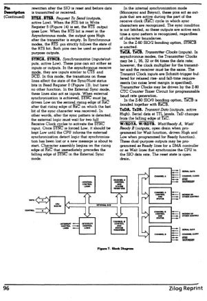
Theory of Operation
The display processor houses the system board, disk drive daughter
board, the CRT, the power supply, and one bus expansion slot.
The system board has the following:
•
Central Processing Unit (CPU)
•
6 to 8k of Read Only Memory (ROM)
•
64k of Random Access (Read/Write) Memory (RAM)
•
Counter Timer Circuit (CTC)
•
Serial Input/Output Controller
(510)
•
Parallel Input/Output Controller (PIO)
•
Two RS-232-C Serial
1/0
Ports
•
Dual 8-bit Parallel Ports
•
CRT Controller and CRT Refresh Memory
•
Speaker
•
Disk Drive Daughter Board Connector
•
Bus Expansion Connector
•
8086 Co-processor
(16/8
system)
•
Parallel Keyboard Interface
CPU
The CPU is a Zilog Z80-A operating with a clock rate of 4 Mhz. It is
initialized to use Interrupt Mode 2 by the ROSR monitor at power on.
The Z80-A also provides refresh to the 64k of dynamic memory on the
system board. Therefore, the I and R registers should not be altered by
an application program.
ROM and RAM Memory
The System Board has two banks of memory. Bank 1 has 64k of RAM.
Bank 0 has up to 8K of ROM.
location FOOOH and RAM (Bank 1) is enabled. Bank 0 is also enabled
when a character is sent to the screen.
6·8k ROM
The CPU board has provisions for 4·2k x 8 Read Only Memory devices.
The first 3 (U33, U34
&
U35) store the firmware for the ROSR monitor.
The fourth (U36) provides translation tables and related firmware for the
position-encoded low profile keyboard.
64k RAM
The 64k byte (65536 x 8) RAM provides space for a portion of the ROSR
monitor (upper 4k FOOOh - FFFFh), and 60k (OOOOh - EFFFh) is free for
programs to execute in such as an operating system and an application
program. This RAM is dynamic and refresh is provided by the Z80-A CPU.
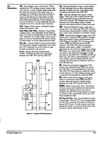
Counter Timer Circuit (CTC)
The CTC has four independently-programmable counter/timer channels,
each with a readable downcounter and a selectable 16 or 256 prescaler.
Downcounters are reloaded automatically at zero. Each channel is
programmed with two bytes. Once started, the CTC counts down,
reloads its time constant automatically, and resumes counting.
Internally, the CTC generates a unique vector for each channel.
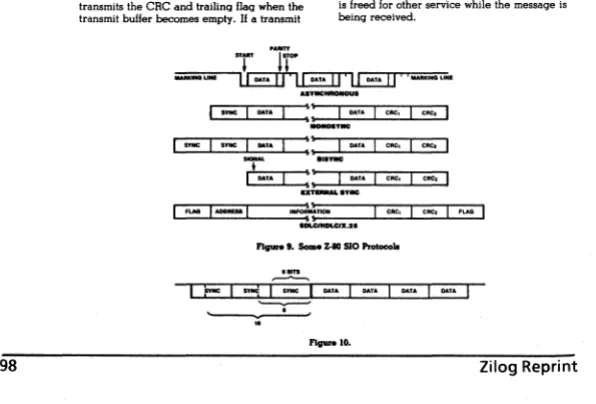
SeriallnputiOutput Controller
(510)
The Serial
110
Controller has two independent, full-duplex channels with
separate control and status lines for modems or other devices. Data rates
are from 50 to 19,200 bits/second. Channel A (modem) supports both
Asynchronous and