· ...
_
-Section 1
INTRODUCTION AND INSTALLATION
'a.e
Introduction ... ... ... ... ... ... ... ... ... ... ... ... ... ... ... ... ... 1-1
InstallaUt)n ... 1-1
Section 1
INTRODUCTION AND INSTALLATION
INTRODUCTION
This document describes the TEK6100 Series ramily or computing systems. This rirst section
provides an introduction along with installation procedures (to be provided). Each rollowing
section discusses individual major subassemblies, ror example Section 2 discusses the
com-puter board and Section 3 discusses the expansion memory board.
INST ALLA TION
This information will be provided at a later date.
Section 2
COMPUTER BOARD
Pale
IDtroductloD ... .... ... ... ... ...
2-1
Computer Board Overview ...
2-1
Board ConneuratloD ... ... ... .... ... ...
2-1
On-Board RAM Configuration Jumpers ... 2-1
Expansion RAM Jumpers ... 2-2
ROM Configuration Links ... 2-2
I(ernel Configurat.ion ... :... 2-2
LAN Interface Jumpers ... 2-2
Special Registers ... ;...
2-2
FUDctloDal Block DescrlptloD ...
2-2
System Bus Structures ... 2-3
Kernel Bus ... 2-3
Internal
Addre~sBus .... ... 2-3
Internal Address/Data Bus ... 2-3
External Bus ... :... 2-3
Kernel (1) ... ... ... ... ... ... ... 2-3
Kernel Bus ... 2-4
Kernel Timing and Control Bus .. ... ... 2-4
Central Processing lTnit ... 2-6
Slave Processor Bus Cycles ... 2-7
~lemory
Management Unit ... 2-7
~1emory
t-.1anagement ... 2-7
Floating Point Unit ... 2-8
Timing Control Unit ... 2·8
Kernel ROM (2) ... 2·8
Non-Volatile Memory (8) ... 2-8
~1ain ~1emory(14) ... 2·8
Memory Access and Refresh Timing (13) ... 2-9
~1emoryAddressing (14) ...
~...2·9
Parity Generation and Checking (14) ... 2·9
System Control Block (9) ... 2-10
Floppy Disk Interface (4, 10) ... 2·10
Erroneous ALE Detection Logic ... 2·11
Hard Disk Interface (3) ... 2·11
Disk Data Cache ... ... 2·11
Burfer Control PAL ... 2·12
Dual RS·232-C Interface (5) ... 2·12
GPIB InterCace (6) ... 2-12
Local Area Network InterCace (12) ... ... 2-13
Interrupt Control ... 2-13
External Bus InterCace ... 2·13
Bus Timeout ... 2·13
DMA Arbitration (2) ... 2-14
DMA Arbitration PAL ... 2·14
Clock Generation (7) ...
~... 2·14
Reset Pulse Stretcher ... 2·14
Time-of-Day Clock
(9) ...
2-14
TABLES
Table
No.
Pale
2-1
RA~1Configuration Jum pers .. ... .... ... ... ... ... ... .... 2.1
m
;:)
III
.
....
~
·1
~ Z ~ 0\ II: lISu W
II) ·ri
c: I- 0
I!! )(
I- W
~ II)
dl
m 0 0 uI- M
~ CQ
II:
'0
I-m ~
lIS
0
CQ ~
QJ .j.J
:J
~
u
'~---~r---J
I
/EXTERNAL 1/0 CONNECTORS
Section 2
COMPUTER BOARD
INTRODUCTION
This section describes the use and operation of the TEK6100 Series computer board. This
document does Dot discuss software interface topics relevent to the computer board. Refer to
the TEK6100 Series OEM Manual for this information.The contents of this section are
organ-ized as follows:
•
Computer Board Overview
•
Board Configuration
•
Functional Block Description
COMPUTER BOARD OVERVIEW
The TEK6100 Series computer board, is a 16032-based processor that provides the computer
resources and base I/O interfaces for t.he TEK6100 Series family of workstations. The board is
a large circuit board located at the top of the system cabinet and contains up to 1 megabyte
of main memory, with an additional 2 megabytes (maximum) available on an expansion
board.
BOARD CONFIGURATION
The board has a number of jumpers and links that must be configured at the factory if the
board is to be installed properly. Jumpers are zero ohm
re~.istorsthat are machine insertable.
Links are small shorting connectors that are installed on .025-inch diameter pins.
ON·BOARD RAM CONFIGURATION
JU~IPERSThere are six jumpers that select the density of the RAM memory chip used on the board.
These jumpers are configured for the applicable memory chip as indicated in the following
table:
Table 2·1
RAM CONFIGURATION JUMPERS
W2141
W2143
W2130
W2131
W2140
W2141
64-kbit chip
remove
install
remove
install
remove
install
256-kbit chip
install
remove
in!'tall
remove
install
remove
COMPUTER BOARD
EXPANSION RAM JUMPERS
A jumper pair is used t.o select whether or not an expansion memory board is used in the
sys-tem.
If
expansion memory is used, jumper WOl51 is installed and jumper is removed.
If
expansion is not used, jumper WOl51 is removed and jumper \\70152 is installed.
ROM CONFIGURATION LINKS
There are two links that establish the density of the ROM chips used, either 64k/128k bit or
256-kbit.
If
the system uses 64 or 128-kbit ROM parts, install links between pins 2 and 3 only
of jumpers J5290 and J5291.
If
the system uses 256-kparts, instaJllinks between pins 1 and 2
only of jumpers J5290 and J5291.
KERNEL CONFIGURATION.
There are rour links that are used to establish whether the MMU is used in the system and
one link that est.ablishes if the FPU is in the system.
If
the MMU is resident, no links are
installed in jumpers J2040-J2042, and J0243.
If
the MMU is not resident, install a link
between pins 1 and 2 of jumpers J2040-J2042, and J0243.
If
the FPU is resident in the system, no link is installed in jumper J0250.
If
the FPU is
resident, install a link between pins 1 and 2 of jumper J0250.·
LAN INTERFACE JUMPERS
Three jumpers select which serial interface chip is used for the LAN interface.
If
the Intel
82501 Serial Interface chip is used, jumpers W8050 and \V8051 are installed, and jumper
\V8052 is removed.
If
the SEEQ 8002 Serial Interface chip is used, jumpers \V8350 and W8351
are removed and jumper \V8352 is installed.
SPECIAL REGISTERS
Refer to the OEM Manual for topics such as software interface, memory maps, system and
1/0
control and status registers, etc.
FUNCTIONAL BLOCK DESCRIPTION
The computer board is divided into several major functional circuit areas or blorks, with each
block performing a general function. This section identifies and discusses the operation of
eaeh functional block. The bus st.ructures that tie the major functional blocks together are
discussed first. The number immediately following the various section titles identifies the
schematic page on which that ruentjonal block of circuitry can be found.
Figure 1·1 is a block diagram showing each of the blocks discussed.
COMPUTER BOARD
SYSTEM BUS STRUCTURES
There are four major buffered bus structures that support data transfer between each
func-tional block and throughout the computer board:
KerDel BUI
This bus supports data transfer within the kernel and is buffered from the remainder of the
system. The kernel is further defined later in this section .
. IDternal Address BUI
The Internal Address Bus (IA Bus) is the latched address portion of the multiplexed Kernel
Bus (see page 9 of te schematic diagrams). This bus provides 24-bit addressing for Kernel
ROM and main memory as well as the system I/O control decoders. Latching is performed by
thrt>e 74F373 octal latches.
IDterDal Address/Data BUI
The Internal Address/Data Bus (lA/D Bus) provides the address and data interface between
the kernel and the various system I/O devices on the compute engine. Interface between the
External Bus and the kernel is also provided by the IA/D Bus. The structure of the 1/
AD Bus
is basically the same as the Kernel Bus: a 24-bit multiplexed address/data bus with the 16-bit
data bus sharing the lower 16 lines of the 24-bit address bus (see page 9 of the schematic
diagrams). The
lAID
Bus is buffered from the Kernel Bus by three 74ALS245 octal bus
tran-sceivers.
E:lterDal BUI
The External Bus provides the interface between the compute engine and system options. Bus
connectors located on the options backplane provide electrical interface. The External Bus
primarily an extension of t.he IA/D Bus. Bidirectional interface for the address/data bus itself
is provided by six 74AS373 octal D-type latches and associated bus interface control logic.
Interface for the bus-control and protocol signals is provided by two 74F244 octal buffer
Iline
drivers (see page 11 of the schematic diagrams.
KERNEL (1)
The kernel controls, either directly or indirectly, the major functions for the entire compute
engine. As stated above, the kernel is comprised of five major components: the Central
Pro-cessing Unit (CPU), the Memory Management Unit (MMU), the Floating Point Unit (FPU),
and the Timing Control Unit (TCU), and kernel ROM. The FPU is an optional device. \Vithin
the kernel, these devices are supported by additional logic. System addressing and memory
management/protection is a task that is shared between the CPU and the MMU, while
float-ing point operations are supported by the FPU.
Data transfer wit.hin the kernel and with the remainder of the syst.em is via the Kernel Bus,
which consists of the multiplexed address and data bus. Another bus apart from the Kernel
Bus is the Kernel Timing and Control Bus, which provides the necessary timing, st.atus, and
control signals between the primary components.
Computer Board
KerDel
BUIThe Kernel Bus provides the means of data transfer within the kernel and between the kernel
and the rest of the compute engine. All signals on the Kernel Bus are high-active. The Kernel
Bus may be sampled at the CPU pinout. Refer to "Central Processing Unit" for CPU pin
assignments or page
1of the schematic diagrams.
Addrel. Bill 16-23. These lines are high-active outputs and are the most significant eight
bits of the Kernel Bus address bus. During clock period Tl, the b'lS contains the virtual
address output by the CPU. During clock period TMMU, this bus contains the translated,
physical address output by the MMU.
Address/Data Bits 00-15. These are the multiplexed, bi-directional address and data lines for
the Kernel Bus. All lines are high-active. Bit 00 is the least-significant bit. During clock
period TMMU, this bus contains the virtual address output by the CPU. During TMMU this
bus contains the physical address output by the MMU. During clock periods T2 through T4,
this bus contains data output by the CPU, MMU, memory, etc.
Kernel TlmlDg aDd CODtrol BUI
This bus is local to the kernel and is used to provide control, timing. and coordination of
kernel-level operations, including memory management, and the execution of floating point
operations. These signals may be sampled at the CPU pinout, which is provided in the
follow-ing section. Bus signals are defined below:
Phase
1,
Phase
2.
These pins provide two non-overlapping phases of a single frequency,
10-megahertz clock, although this clock may be slowed to 5 10-megahertz for big build. These
inputs are taken from the Timing Control Unit. The execution of microinstructions within
the CPU or steps in a data transfer over the Kernel Bus is synchronized and controlled with
respect to the number of Timing states or T states required to complete the execution.
A
T
state is defined as the wavelength of the Phase
1
clock input. T states are numbered
progres-sively from the beginning of a bus cycle to it's completion.
Ready-I. This is a high-active signal that is asserted by the Timing Control Unit at the end
of the bus cycle to signal the CPU that the operation is complete. The CPU then terminates
the cycle. An external device that requires additional time to finish the bus cycle can request
an extension to the TCU. The
Teu
will then insert a given number of wait states, allowing
the device to finish the cycle before asserting Ready-I.
Hold Request.O. This low-active input is asserted by another device (MMU) that is requesting
the use of the Kernel Bus.
If
the CPU complies, the CPU asserts Hold Acknowledge-O to the
MMU, thereby granting the bus to the MMU. Hold Request-O is asserted for the entire time
the MMU has the bus and Hold Acknowledge-O remains asserted by the CPU until the bus is
regained by the CPU. This handshake sequence allows the MMU to acquire the bus and place
the translated address on the bus. See the following definition.
Hold Request AckDowledge. This low-active output is asserted by the CPU to grant the bus
to another device on the Kernel Bus (MMU). This signa) is asserted after the MMU has
asserted Hold Request-O. Both signals remain asserted for the duration of the bus cycle, after
which the MMU deasserts Hold Request-O and the CPU regains control of the bus by
deassert-ing Hold Request Acknowledge-O. See the previous definition.
Com puter Board
High Byte Enable-O. This low-active output is asserted by the by the CPU to enable the high
byte of the addressed location to be placed on the bus. Memory is organized as t\'70 eight-bit
banks, with each bank receiving the 24-bit address in parallel. The low bank (bits
000-007)
responds to even byte addresses, that is when the least-significant address bit (AOO) is low.
The high memory bank (bits
008-015)
is enabled when High Byte Enable-O is asserted. This
feature permits the addressing of individual bytes even though the data bus is 16-bits wide.
Data Strobe-OlFloat-O. This is a dual-function pin, the function of which is determined by
whether or not the MMU is performing address translation or the CPU is addressing .the
Ker-nel Bus directly. For bus cycles that are not address-translated, this pin functions as a Data
Strobe-O output from the CPU. Data Strobe-O is asserted after the multiplexed address/data
bus has switched from address presentation to accepting or presellting data. The assertion of
Data Strobe-O validates the data on bus lines ADOO-ADI5. Since address translation is always
performed for every bus cycle initiated by the CPU, Data Strobe-O is never asserted.
For bus cycles that are address-translated, this pin functions as the Float-O input to the CPU.
The assertion of Float-O by the MMU causes the CPU to wait longer than the normally
allot-ted TMMU T state for the MMU to perform address translation. This function is employed
by the MMU in order for it to update its internal translation cache from page tables in
memory, or to update status bits contained within the tables. Timing states are not numbered
during a float condition, and the entire bus cycle is placed on a temporary hold. After Float-O
is de asserted, the bus cycle continues from where it was suspended. The Kernel has been
implemented such that address translation is always performed by the MMU, although the
translated physical address may be the same as the virtual address.
Reset-O/Abort-O. This is a low-active, dual-function input.
If
this signal is asserted during
TMMU or TFloat (an address-translated cycle) and held low for one clock cycle, this pin
causes an A bort of the bus cycle and the instruct.ion that executed it. The rest of the system
remains unaware of the aborted cycle, since the MMU Physical Address Valid-O address
strobe, which triggers the physical cycle, was not yet asserted.
If
this pin is held low for at least 64 clock cycles a Reset is initiated.
Address Trans:lltlon-O/Slave Processor Control-O. AT-O/SPC-O is a bidirectional, dual
func-tion signal. The AT-O porfunc-tion of this signal enables address translafunc-tion by the MMU. The
SPC-O function enables slave processor communications (ie, with the FPU).
The CPU is able to operate with or without address t.ranslation. The mode of operation is
determined by the presence of the MMU. The MMU asserts Address Translation-O during
reset and at power up. The CPU samples AT-O on the rising edge of the reset pulse.
If
the
AT
-0
is high (no
M
MU present), bus cycles are performed without address translation.
If
dur-ing reset AT -0 is low, the bus cycle includes an extra clock cycle (TMMU). At this point, the
DS-O/FLT-O signal becomes a Float-O command input to the CPU (see previous definition of
DS-O/FLT-O).
AT-O/SPC-O is also used as the data strobe in slave processor data transfers. During slave
processor data transfers, data is transferred on bus lines ADOO- AD15, but no bus control lines
other than DDIN-O (controlled by the CPU) are asserted. For example, ADS-O, HBE-O, ect,
are not used. During a slave processor bus cycle, the slave processor samples the CPU status
lines STO and STI on the leading edge of SPc-o. During a data read, SPC-O remains asserted
until data has been read from the slave processor. During a uata write, the slave processor
latches the status bits on the leading edge of SPc-o and latches data on the trailing edge of
SPc-o. In all slave processor bus cycles, SPc-o is asserted by the CPU. Refer to Slave
Proces-sor Bus Cycles.
Computer Board
User-l/Supervlsor-O. This output is taken rrom the U bit in the Processor Status Register,
which is an internal status register. Asserted high, this signal indicates that the CPU is
run-ning in the user mode. Asserted low indicates the 8upervisor. This signal is sampled by the
MMU ror mapping and protection purposes.
Address Strobe-O. Address Strobe-O (ADS-O) is asserted by the CPU when it places an
address on the Kernel address bus. Without the MMU, this signal would be used to validate
and latch the address. However, with address translation by the MMU, this signal is sent to
the MMU only, where it latches the virtual address. The MMU outputs the Physical Address
Valid-O strobe to validate the translated, physical address.
Physical Address Valld-O. This MMU output is generated during TMMU and is used as the
address strobe to latch the physical address into external memory devices. This signal is also
used during a rIoat condition to access the external page tables.
Data Direction In-O. Data Direction In-O (DDIN-O) is output by the CPU or the MMU to
specify a read operation (low) or a write operation (high). During normal bus cycle with
address translation, this signal is output by the CPU to indicate data direction. During a (loat
condit.ion, the CPU tristates DDIN-O, allowing the MMU t.o assert DDIN-O low, thus allowing
the MMU to updat.e its page tables rrom memory. The MMU also controls DDIN-O when it has
control or the Kernel Bus.
Procram Flow Status·O. This low-active pulse is asserted by the CPU to indicate the
begin-ning or an instruction cycle.
Status STO·ST3. This is a rour-bit bus cycle status code that provides status information.
The pins are interpreted as a rour-bit value, with STO as the least-signiricant bit. Only two
bits, STO and STl, are sampled by the FPU during slave processor bus cycles. Rerer to the
CPU data manual ror a derinition of each of the codes.
Interlocked Operatlon.O. This is a low-active output that is asserted during a Set Bit,
Inter-locked or Clear Bit, InterInter-locked instruction. This signal is used to reserve the bus in a
multi-processor system that shares resources, in this case, common RAM that the compute engine
shares with the display engine.
Non-Maskable Interrupt·O. The Non-Maskable Interrupt-O (NMI-O) is a low-actiye input to
the CPU.
Central Processing Unit
The NS16032 CPU (U1280) is the heart of the kernel. This device is configured in a 48-pin,
dual-in-line package. The CPU provides a I6-megabyte unirorm address space. The CPU's
internal architecture features 32-bit data paths, although the data path at the pin-out is
16-bits wide. Rerer to page 1 or the schematic diagrams.
The CPU provides 16 registers, eight or which are dedicated control/status registers, and
eight general purpose registers. The general-purpose registers are 32-bits in length and are
used ror general storage requirements, such as storing temporary variables and addresses. The
CPU clock rrequency is 10 megahertz. As stated previously, data transter within the
com-puter board is arrorded by the Kernel Bus and other bus structures. Within the Kernel
how-ever, dedicated data transrer that is transparent to the rest of the system is accomplished via
the slave processor bus cycle.
Computer Board
Slave Processor Bus
Cycles.
The slave processor bus cycle permits communication between
the CPU and the sla'\'e processors (the MMU and the FPU) without executing the Kernel Bus
protocol. This type of transfer utilizes the data bus portion (ADOO-AD15) but none of the
bus control/signals (excluding DDIN-O).
Slave processor bus cycles require only 2 clock cycles or T states (labeled Tl and T4) to finish.
At the start of a data read cycle (Tl), the CPU places the appropriate status code on lines
ST3-STO and the appropriate processor identification byte on data line ADOO-AD07 of the
Kernel Bus. The CPU then asserts SPC-O. Both the FPU and the MMU decode the ID byte
and latch the status from the CPU on the leading edge of SPC-O. The appropriate slave
pro-cessor responds by placing data on lines ADOO-AD15 at T4. The CPU
rea&~the data and
ter-minates the cycle by deasserting SPC-O.
During a data write (at TI), the CPU places the appropriate status code and processor ID on
data lines ADOO-AD07, as before. The CPU then asserts SPc-o and the appropriate processor
responds by latching the status and ID byte. The CPU then removes the ID byte from the
Kernel Bus and places data on the bus. The data is latched by the slave processor on the
trail-ing edge of SPC-O as it is de asserted (T4). At the end of a data write, the slave processor
sig-nals a successful transfer by pulsing SPC-O low.
Since ADS-O is not asserted by the CPU, none of the other nssociated bus protocol signals are .
asserted. The CPU, however asserts DDIN-O as appropriate. In both of the above cases, the
status code is set up by the CPU during the previous clock cycle.
Memory Management
Unit
The NS16082 Memory Management Unit (MMU) (UI300) provides support for demand-paged
virtual-memory management. The chip, in concert with the CPU, permits rapid address
translation and protection on individual 512-byte memory pages. The chip uses a associative
cache that stores the 32 most frequently used memory page table entries. The MMU is
pack-aged in a 48-pin, dual-in-line configuration. Refer to page 1 of the schematic diagrams.
Memory Management. For,addressing purposes, memory is divided into several 512-byte
pages. Associated with each page of memory are page tables that. the MMU and t.he operating
system maintain in physical memory. The page tables contain information pertinent to each
memory page, such as the page access permission codes, whether the page has been accessed,
and if it has been written to. Also contained in the page tables are values that are used to
arrive at the physical address. The MMU executes a translation algorithm that determines the
validity of the access and provides the physical address. Of the virtual address provided by
the CPU, the least-significant 9-bits are not modified. These 9 bits provide discrimination to
the byte level within t.he 512-byte page.
By modifying the page tables as required, the operating system controls the mapping of
vir-tual addresses to physical memory. Additionally, the operating system can control the degree
of access (read or read and write) permitted to specific pages in the supervisor and user modes
by generating translation error aborts if access permission codes are violated.
The most frequently referenced or accessed page tables are stored by the MMU in an internal
cache memory, thus saving the
M~1Ufrom having to retrieve the page table from memory for
the majority of accesses. The cache contains 32 page table entries.
Ir
during a bus cycle, the
given access is not a "hit", the MMU asserts the Float-O signal to the CPU, which
tem-porarily suspends the bus cycle while the MMU retrieves the page table rrom physical memory
via the Kernel Bus. Once the page table entry has been retrieved, the least-used entry is
removed from the cache and the newest entry is placed in the cache. The Float condition is
terminated and the bus cycle
contin~es
from where
it
was suspended.
Computer Board
All bus cycles initiated by the CPU are address-translated, however in some cases the
translated, physical address may equal the virtual address placed on the Kernel Bus by the
CPU.
Floating Point Unit
The NSl6081 Floating Point Unit (FPU) (UI260) operates as a slave processor and performs
both single precision (32-bit) and double precision (64-bit) aritbmetic. This device is
pack-aged in a 24-pin configuration. Data transfer between the CPU and the FPU is not
accom-plished using tbe normal Kernel Bus protocol, but the slave communications protocol
described previously. The FPU contains 9 32-bit registers, eight of which are general-purpose.
The ninth register is a status register. Refer to the FPU data sbeet for additional information
and pat;e I of the schematic diagrams.
Timing Control Unit
The NSl6201 Timing Control Unit (TeU) (U0320) is a 24-pin DIP that provides the
two-phase 10 megahertz clock output based on the 20 megahertz crystal frequency, as well as
several signals that support Kernel Bus logic, timing and control functions. The TCU also
provides for a ,oariety of bus cycle extensions to compensate for slower devices (compute
engine or peripheral devices). Refer to the TeU data sheet for additional information and
page I of the scbematic diagrams.
Kernel ROM (2)
Up to 128 kbytes of Kernel ROM are provided by four 256-kbit (32k x 8) EPROM chips
(U3280, 3300, 4280, and 4300). Kernel ROM is organized as two, 64-kword banks. Lesser total
capacities are 64 kbytes and 32 kbytes, depending on chip density. Addressing is provided via
the Internal Address Bus, which is the latched address portion (ADOO-ADI5) of the Kernel
Bus, while ROM data is placed directly on
the
Kernel Bus data bus. Refer to page 2 of the
schematic diagrams. Kernel ROM is discussed further in Section Five of the TEK6100 Series
OEM Manual.
NON-VOLATILE MEMORY (8)
This block consists of two 256-bit, non-volatile, sequential-access EEPROMs (UI43, UI44)
and a Non-volatile-Memory Control Register (UI08). Each memory chip is organized as 16
registers containing 16 bits each. Each register is read from serially.
MAIN MEMORY (14)
Main memory provided on the computer board consists of up to 1 megabyte of dynamic RAM
using 256-kbit parts, or 256 kbytes using 64-kbit parts. The board contains a maximum of 36
RAM chips, each of which is organized in a 256 k by I-bit or 64 k by I-bit format. On the
board, memory is organized as two rows, each containing a maximum of 18 chips. Each
memory row is two-bytes wide plus one parity bit per byte. Jumpers that select the chip
den-sity and board capacity, as well as whether or not the sytem is equipped with an expansion
memory board, are discussed in tbe a previous section of this document, titled Board
Confi-guration.
The computer board contains logic that provides support functions for the RAM. These
(unc-tions are: memory access and refresh timing, memory addressing, and parity generat.ion and
error detection.
Computer Board
Memory Access and-Refresb TimID. (13)
This logic coordinates the memory refresh cycle, which is performed every 12.5 microseconds,
and normal memory accesses. The Refresh Clock operates a 80 KHz and initiates a memory
refresh cycle on the rising edge of the clock pulse, at which time various status lines that
indi-cate an impending data transfer are sampled. U the status lines are asserted, the refresh is
postponed until the data transfer is completed. When refresh is in process, memory access are
locked out until the refresh is completed.
This logic employs a 200-nanosecond delay line to establish memory-access and refresh-cycle
timing. The data read cycle from memory requires approximately 400 nanoseconds, whereas a
data write cycle from memory can be extended beyond 400 nanoseconds.
This logic supports a distributed refresh method whereby only one memory row is refreshed
per refrt'sh cycle. The next refresh cycle increments the refresh address counter by one in
preparation for that cycle. The counter is incremented on the trailing edge of the Refresh
, Clock. After the new row address has been placed on the Memory Address Bus (MA Bus), the
Row Address Strobe (RAS-O) is pulsed, refreshing the 512 memory-bit locations in that row.
With 256 k-byte parts, 512 refresh cycles are required for a full memory refresh.
Memory Addressing (14)
This block samples the IA/D lines 18-23 to determine if the bus cycle is a memory access, in
which case the impending refresh cycle is may be postponed until the end of the data transfer.
This block also provides the multiplexing required to place the 16bit address word (lA/DOl
-IA/DI6) on the 9-bit Memory Address Bus (MAO - MA8), as well as the Row Address Strobe-O
(RAS-O) and Column Address Strobe-O (CAS-O) synchronization required to latch the address
into memory.
Parity Generation
DndCbecldnl (14)
This block utilizes two parity generators/checkers and associated logic to generate and store
an odd parity bit for each byte during a memory write operation, and to check the stored
par-ity bit during a memory read.
If
an error is detected during a read, a Parity Error signal is
generated, as well as a bit defining whether the error applies to the high or low byte. A Parity
Error Register, which is continually loaded with the current memory address, is used to
pro-vide the address of the faulty memory location. A brief description of the operation of the
parity generation and checking logic for the high byte is given below:
During a memory write, the high data byte from the IA/D Bus is input to the U25 parity
generator/checker. At this time, the octal D-type latch U140 is disabled by status signals that
are set as a function of the type of data transfer, read or write. Nand gate U139 outputs a
high at pin six, and the parity generator U25 generates even parit.y for the data byte plus t.he
additional high bit input at pin 4. This parity bit is equivalent to odd parity for the data
byte, and the parity bit is stored with the byte in memory.
During a memory read, the octal latch U140 is enabled and the stored parity bit is inverted by
nand gate V139 and input at pin four of parity generator U25. U25 generates parity for the
data byte plus the inverted parity bit.
If
the stored bit or the data byte is in error by one bit,
the parity checker generates an even-low parity bit, thus signaling a parity error.
COMPUTER BOARD
SYSTEM CONTROL BLOCK (9)
The system control block provides the system I/O enables and control signals required to
enable DMA transfers via the various I/O devices, as well as the enables for the System
Con-trol Register and the System Status Register. These enables are arranged as memory-mapped
I/O locations in the ker.nel's external memory space. This logic consists primarily of two
74F138 3-to-8-bit decoders.
This block also contains the System Control Register (octal D-type flipflop U18) and the
Sys-tem Status Register (octal D-type f1iprIop UI9), along with the enables required to drive these
registers (as given above).
The system control block also provide'S a mechanism for low-level debugging of the board.
This consists of a diagnostics switch register and a diagnostics display register. The switch
register is a 8-switch DIP that corresponds to lines ADOO-AD07. The setting of the switch is
read by enabling 74F244 octal buffer U16 (address FFF008). Diagnostic information is
displayed by a write to the same address. An 74LS273 octal D-type f1iprIop performs as the
display register. The D outputs (ADOO-AD06) correspond to segments A-G of a seven-segment
display. Bit AD07 drives the decimal point.
FLOPPY DISK INTERFACE (4, 10)
The rJoppy disk interface is composed of two major LSI components: the WDI770 Floppy
Disk Controller (U7020) and the AM9516 DMA Controller (U8290), along with supporting
logic. The \VDl770 is a rIoppy disk controller and
formatt~rand also contains digital data
separation logic and write precompensation circuitry. The \VDI770 is a 28-pin DIP. There are
six registers within the floppy disk controller that allow the Am9516 DMA controller to
exe-cute data transfer between the disk controller and the DMA controller. These registers
con-tain command and status information, various head positioning information, and 8-bit data.
Interface between the two controllers is via an 8-bit bidirectional data bus and various control
signals.
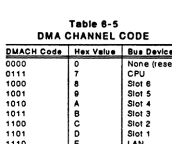
The DMA controller (page 10 of the schematic diagrams) is equipped to handle two separate
channels although only one DMA channel (channel
B)
is used. DMA operations are initiated
by the kernel by loading DMA control parameters into a control block known as the Channel
Control Table. The Channel Control Table is maintained by the kernel in main memory. The
kernel then places the starting address of the Channel Control Table in the Chain Address
Register (internal to the DMA controller) and issues a "Start Chain" command to the
con-troller. The
D~IAcontroller responds by updating its various internal control registers with
the control parameters located in the Channel Control Table. The Channel Control Table
contains such information aft what specific registers are to be updated or reloaded, the source
data
addre~s,the destination data address, e-ct.
"Chaining", allows the several DMA transfers to be performed asynchronously. This method
places the address of the next Channel Control Table in the within the previous table, so that
when a given DMA operation is completed, the DMA controller reads the new address or the
control table, updates internal control registers with the table, and executes the new
com-mand.
The DMA cont.roller also performs byte/word alignment between the 8-bit disk data bus and
the 16-bit IA/D Bus. As mentioned before, the System Control Block provides the address
decoding required to access the floppy disk interface.
Computer Board
ErroDeoul ALE DetectloD LOllc
Logic associated with the AM9SI6 DMA Controller includes erroneous ALE detection logic.
This consists of the D-type flipflops U604I, U6130 and associated logic. This logic was
impli-mented in order to detect and void or cancel the erroneous assertion of Address Latch
Enable-l by the controller. This logic differentiates between chain operations and single data
transfers. Note that this interface allows only single data transfers per
bus-request/bus-release cycle. This logic operates as follows:
The Normal/System-O output from the DMA Controller is programmed to be asserted high
w hen data is being transferred between the controller and the host. During a data transfer,
ALE is asserted by the controller to the Kernal Bus as Kernal Physical Addrss Valid-O
(KPAV-O). \Vhen data is placed on the bus, Normal is asserted by the DMA Controller, which
is clocked through U6041 as NOALE-O. NOALE-O disables AND gate U3140 and Quit ALE-1
(QALE-) de asserts KP A V-O to the Kernel Bus.
During chaining operations, System-O is asserted by the DMA Controller, which is clocked
though U60410 and U6130 as Hold Bus-O (HLDBUS-O). In this case, Bus Request has been
released and there is no data strobe. Disk Data Strobe-O is asserted as Memory Data Strobe-l
(MDS-1) in order to complete the bus cycle. Since the DMA Controller is executing reads from
memory during chaining operations, memory data is not affected.
HARD DISK INTERFACE (3)
The hard disk interface is composed primarily or the WDI010 \Vinchester Disk Controller
(U7100), an external 4-kbyte cache, a DP8460 data separator and a Hard Disk Control
Regis-ter.
The controller perrorms the normal functions or a hard disk drive controller/rormatter,
although it does not feature write precompensation and this logic (consisting of quad D-type
flipflop U47, delay line U51, and data multiplexer U52) is implimented externally.
On the drive side of the controller, the data separator receives MFM encoded data from the
disk drive and separates this data into synchonized data (SDATA) and a Read Clock (RCLK)
signal. The disk controller decodes this serial data from RCLK into 8-bit parallel data. During
a write to the disk, data is MFM-encoded by the controller.
Disk Data Cache
On the host side of the controller, the 4-kbyte cache is a serial, disk-data transrer buffer that
is accessible by the disk controller or the kernel. The buffer appears to the kernel as a
2-kword (16-bits) sequential-access bufrer. The buffer itself consists of two 2048 x 8-bit st.atic
RA.M chips,
V156
and
V157.
This burrer and octal bus transceiver
V159
also serve as a data
assembler/disassembler in that data is t.ransrerred between the kernel and the buffer in 16-bit
words, whereas data transfer between the burrer and the disk controller occurs in 8-bit bytes.
Buffer addressing is performed by two dual, four-bit binary counters,
VI55
and U99. Only
. half of
V99
is used. During a data write to the disk, the kernel clears the buffer by setting the
Manual Clear bit in the Hard Disk Control Register (octal D-type flipflop VIS8). This
gen-erates the Counter Clear (CCLR) output of the Buffer Control Programmable Array Logic
(PAL) chip U44, which clears the counter. As each 16-bit word is loaded into the burrer, the
counter is incremented by the Counter Clock (CCLK) output of PAL U44, which develops the
dock from the Data Strobe-O input. When the kernel has loaded the buCfer, the kernel writes
a Manual Ready-l signal to the controller via the PAL (input to the controller as Hard Disk
Bufrer Ready-O (HDBRDY-O)). The controller then clears the bufCer counter and transfers the
Computer Board
contents of the buffer to disk, incrementing the buffer address counter as each 16-bit word is
read. Since the buffer is organized as two 2k x 8·bit chips, each byte can be read individually
by
the controller. This is permitted by the bus transceiver UlS9, which multiplexes both the
high and the low bytes of the buffer onto Hard Disk Data lines 0-7 (HDDO-HDD7).
During a data read from the disk, the controller clears the buffer address counter and begins
loading the buffer. This time the bus transceiver operates in reverse fashion, demultiplexing
the 8-bit data from the controller into the high and low bytes prior to loading into the buffer.
CCLK is gene:ated by Burfer Chip Select-O output from the controller, via the PAL. \Vhen
the controller-to-bufrer transfer to completed, the controller signal the kernel by asserting
Hard Disk Interrupt-I. The kernel proceeds to read the contents of the bufier, by first
reset.-ting the buffer address counter and then incremenreset.-ting the counter with each word read.
Two 74LS245 bus transceivers (U45 and U46) serve to buffer or isolate the
lAID
bus (rom
disk/cache data. As given previously, the System Control Block provides the address decoding
required to enable data transfer via the hard disk interface.
Butter CODtrol PAL
The Buffer Control PAL (U8050) controls the operation the disk data buffer and the data
buffer address counter. Inputs to the PAL are rrom the disk controller and the system control
logic (address decode). Outputs drive the buffer chip enables, address counter, and Controller
Ready-O line.
DUAL RS·232·C INTERFACE (5)
The RS-232-C interface is a dual-channel, serial asynchronous DCE port that utilizes the
AM8530 Serial Communications Controller (U6340). The output driver for each port is a
DS1488 transmission line driver. The receiver for each port is DS1489 transmission line
receiver. All configuration, control, status, and data registers are internal to the controller.
Serial port enables are address-decoded by the System Control block. A 4 MHz clock
developed by the clock generator is supplies to the controller.
GPIB INTERFACE (6)
The GPIB interrace utilizes the TMS 9914 GPIB Controller and the SN75160 and SN75162
bus transceivers. This interface supports talker, listener, and controller functions. This design
does not incorporate DMA support and the transfer rate is limited by the speed of the
pro-grammed data transfer. System control or the bus is provided via a GPIB Control Register
(U36). which is a 7 4LS 174 hex D-type flipflop. The System Control Block provides the address
decoding required to enable GPIB I/O operations.
Communication between the controller and the kernel is performed via 13 memory-mapped
registers that contain status and control information, data. These registers are contained
within the controller. Three Register Select lines (RSO-RS2) address one or eight possible
locations, each of which contain one read andlor one write register. Register selection within
the addressed location is a function of the operation: read or write.
On the host side oi the controller, data interrace is 8-bits wide over lines IA/DO-IA/D7. As
stated previously, there is no DMA support for this port.
The 75162 octal bus transceiver U35 drives and receives the GPIB control bus lines, while a
751600 octal bus transceiver U34 dt:ives and receives the 8-bit port data.
Computer Board
The GPIB Control Register contains a GPIB Enable bit (bit lA/DO) that disables the GPIB
bus transceivers and also enables the bus bufrer gate U98. U98 permits the kernel to test the
GPIB protocol sequence of the TMS9914 controller by writing test bits to the control register.
LOCAL AREA NETWORK INTERFACE (12)
The Local Area Network (LAN) interface consists primarily of the 82586 LAN Controller
(8310) and the 82501 Serial Interface Chip (U9370). The primary runction of this port is to
provide an interface between system memory and the LAN link. The host initiates a transfer
over the LAN by the writing the transfer parameters to a control block residing in syst.em
memory. Once the control block is configured, t.he host toggles the Channel Attention line to
the LAN controller by writing the appropriate address to the system control decoders. This
causes the LAN controller to copy the contents of the control block inte internal memory and
execute the command. The controller signals the completion of the transfer by asserting an
interrupt to the host. The LAN controller is a bus master of the IA/D Bus and most of the
DMA t.ransfprs are execut.ed with the LAN directly accessing system memory. For this
pur-pose, 256 kbytes of system memory are reserved for the LAN. The LAN interface is tested via
the System Control Register. Refer to page 12 of the schematic diagrams.
The 82501 Serial Interface chip provides the 10 MHz transmit clock for the 82586 controller,
performs the encoding/decoding of the transmitted/received frames, and provides the
electri-cal interface for the Ethernet transceiver cable.
INTERRUPT CONTROL
The Interrupt Control Unit (ICU) and associated logic provide interrupt management for the
CPU. This logic handles up to 15 prioritized interrupt sources from t.he various intelligent I/O
devices wit.hin the system. Six interrupt lines handle computer board I/O devices, two lines
handle the MMU and FPU, and seven interrupt lines are reserved for optional devices
operat-ing on the External Bus. The ICU resolns interrupt priorities and issues a byte-wide
int.er-rupt vector to the CPU. This device is configured in a 40-pin DIP configuration. Refer to page
12 of the schematic diagrams.
EXTERNAL BUS INTERFACE
This block provides the interface between the Interal Address/Data Bus and the External
Bus. The block consists of primarily of a Bus Interface Control PAL (U6290), six octal D-type
latches used as bus buffers, Bus Timeout Logic, and associated logic. The Bus Interface
Con-trol PAL monitors various system status and conCon-trol signals and conCon-trols the direction and
enable signals required to control the bus buffers.
Bus TlL3eout
This block also handles bus timeout control. The bus timeout counter is started by the
asser-tion of System Address Strobe-} (SAS-I) and is clocked by a 400 KHz clock. The counter is
cleared by the normal execution of the bus protocol within the time required. The counter is
also cleared by a reset. The bus-timeout period is approximately 10 microseconds. The
com-plete bus-timeout cycle takes about 20 microseconds; 10 microseconds are alloted for the
faulty DMA device to release the bus after the associated Bus Grant signal has been
deassert.ed by the host.
COMPUTER BOARD
DMA ARBITRATION (2)
This block performs DMA arbitration for the six available External Bus options slots, and the
computer-board based LAN port and fJoppy disk drive interface. Each bus-request line is
weighted at a particular priority level. Simultaneous External Bus bus requests are arbitrated
according to the priority level assigned to each request line and a bus-grant signal is issued to
the arbitrated requester. This block also generates a 4-bit code (via the 74LS140 8-t0-3 line
en~oder
U70) that is loaded into the System Status Register and indicates the most recently
Uf,ed DMA channel. This code is used after a bus timeout to identify the faulty DMA device.
DMA ArbltratloD PAL
DMA arbitration is performed by a 24-pin DMA Arbitration PAL (UI230) and associated
logic. The PAL monitors the various prioritized bus-request
signa~sfrom the External Bus
option boards, the floppy disk DMA controller, and the LAN interface, and issues a bus grant
to the highest-priority requester.
CLOCK GENERATION (7)
The clock generation logic develops most of the clock pulses required by the system. The
pri-mary clock source is a 20 MHz clock taken from a crystal oscillator. Three 74LS390 4-bit
counters divide this pulse into a 10 MHz clock, a 1 MHz clock, an 80 KHz refresh cIock, and a
200 Hz ICU clock. A secondary crystal oscillator operating at 16 MHz is used to develop an 8
MHz clock and a 4 MHz clock.
Reset Pulse Stretcher
Resets are generated by any device on the External Bus, the power supply, and the Interrupt
Control Unit. All resets pulses are expanded by 2 milliseconds by the pulse-stretching logic
shown on page
7.
This logic consists binary counter U6301, quad nand gate U6270 (shown in
four locations), and inverter U6320. U6301 is employed as a flipflop that is set when Received
Reset-O (RRSET-O) is first asserted. Two milliseconds later the counter U6301 resets the
flip-flop, which des asserts External Reset-O. Reset signals from the ICU (Insane-O) and power
sup-ply (PSINIT-O) are placed on the External Reset-O path. This allows them to be input to the
clock generator block as Received Reset-O, and the Reset Pulse Stretcher operates in the same
fasion as described above.
TIM:E·OF·DA Y CLOCK (9)
This block consists of a MM58167 microprocessor-compatible real-time clock and a 32.768
KHz reference crystal oscillator. The clock contains a real-time counter, 56-bits of RAM, two
interrupts, and a comparator. The RAM is used during power-down storage and as the alarm
latch for comparison to the counter. Address interface with the CPU is via the five low-order
bits (IAO-IA5) of the latched Internal Address Bus. Data interface with the CPU is via the low
byte of the Internal Address/Data Bus. Battery back-up is provided for the clock by a 3 volt,
1200 milliampere/hour lithium battery and associated power-rail logic.
Section 3
EXPANSION MEMORY BOARD
Pale
IDtroductJoD ... ... ... ... ... ...
3-1
EJlpaDSloD l\femory Board Overview... ... ...
3-1
Board CODnguratloD ... ... ... ... ... ... ... ... ... ...
3-1
FUDctloDal Block DescrlptioD ...
3-1
External Bus Interrace Logic ... 3-2
Memory Address Decode Logic ... 3-2
Control and Status Register ... 3-2
Memory Access and Refresh Timing ... 3-3
Refresh Logic ... ... ... ... 3-4
Parity Generation and Check Logic ... 3-4
Memory Address ... 3-4
Memory Data Buffer ... 3-4
Memory ... 3-4
FII·
No.
3-1
3-2
ILLUSTRATIONS
The Control and Status Register During CSR Write
The Control and Status Register During CSR Read
TEK6100-Series Hardware Descriptions
Page
3-2
3-3
~ Generation Parity
r----
...
~ and Detection
<=)
External Bus ~-;
I . - . ,rv-
OPTION BUS A J..Interface
..
Data (Memory Dat9 Buffer
"
" Memory~ Memory
p
~
Memory AccessAddress -v and
~ DecOde Refresh
Timing
I==-
Memory~ Addressing
I
~ Memory Refresh Address
Section 3
EXPANSION MEMORY BOARD
INTRODUCTION
This section discusses the use and operation of te Expansion Memory Board ror Big Build.
This discussion does not necessarily apply to the final production product. This contents of
this section are organized as follows:
•
Expansion Memory Board Overview"
•
Board Configuration
•
Functional Block Description
EXPANSION MEMORY BOARD OVERVIEW
The Expansion Memory board is a double-wiclth option board that provides additional main
memory for the TEK6100 workstation. The amount of memory provided by the board is
dependent on the density of the memory chip used. Using 64K X 1-bit memory chips provides
256K bytes of memory in a fully populated board. Using 256K x I-bit chips provides 2
mega-bytes on a fully populated board. (The Big Build version of this board uses 64-kbit chips only)
BOARD CONFIGURATION
The Big Build version of this board will use 64-kbit chips only.
If
necessary, refer to the
schematic diagrams for jumper information. Additional configuration information will be
pro-vided at a later date.
FUNCTIONAL BLOCK DESCRIPTION
The Expansion Memory board is comprised of eight major functional blocks that are listed
below and discussed in the rollowing paragraphs:
•
External Bus Interrace Logic
•
Memory Address Decode Logic
•
Memory Access and Rerresh Timing
•
Refresh Logic
•
Parity Generation and Check Logic
•
Memory Address Logic
•
Memory Data Burrer
•
Memory
EXPANSION MEMORY BOARD
EXTERNAL BUS INTERFACE LOGIC
This block provides the electrical interrace between the Ext.ernal Bus and the Option Bus
located on the Expansion Memory board. This function is performed by a 74F373 octal D-type
flipflop (1lI02) and two 74ALS245 octal bus transceivers (U9I03 and U9104) along with
asso-ciated logic. UI02 latches bits 16-23 of the address word, while U9103 and UOI04 provide
bidirectional interface for bits ADOO - AD15 of the External Bus.
MEMORY ADDRESS DECODE LOGIC
Address decoding for the memory board is provided by a 25LS251 equal-to comparator
(U9105. which decodes the memory board CSR address) and the U9113 programmable array
logic (PAL) chip.
The comparator decodes the CSR address by comparing the predetermined Status Select
Lines SSO-SS4 with bits 11-15 of the Option Bus. A match selects the memory board CSR.
Data is latched into the CSR on the trailing edge of Data Enable (DEN-I). DEN-1 is the
inverted equivalent of External Data Enable (EDEN-O).
The PAL U9113 decodes bits 17-23 of the address word and outputs the appropriate bank
select signal to memory, as well as an additional memory-access control signal. The PO-P2
sig-nals input to the PAL define a 3-bit program code that is loaded into the CSR by the host.
This code is used to map the memory into the desired address space. The U9Il3 PAL is also
used during memory refresh in the generation of the row address strobes.
Control and Statns Register
The passing of status and control information between the host and the memory board is
per-mitted by the Control and Status Register (CSR). The CSR is a 16-bit read/write register
that consists of a 74LS273 octal D-type flipflop U9120, and two 74ALS244 octal bus
tran-sceivers (U9121 and U9122).
The contents of the CSR is dependant whether the host is writing to the CSR or reading from
it. During a CSR write, the host loads the CSR with memory mapping program bits (PO-P2)
and parity logic control bits. During a read from the CSR, bus transceivers U9121 and U9122
permit the host to read the mapping program bits, parity status information, and a code that
defines the option type.
The contents of the CSR during a CSR write is defined below:
DI5
D14-D12
Dll
DIO
D09
D08
D07-DOO
N.U.
P2-PO
N.U.
N.U.
PBAD-l
PARE-l
N.U.
Fiaure 3-1. The Control and Statui Reaister Durina CSR Write.
Expansion Memory Board
Program Blu P2·PO. This is a 3-bit code that is used by the host to map the memory board
into the desired location within addres" range of the host. There are eight possible mapping
locations.
PBAD·I. PBAD-I (Parity Bad-I) is a parity logic test bit that is set by the host to force the
generation of bad parity during a memory write. The host then reads (rom the same location
and generates valid parity, and then compares the stored parity value against the valid bit.
PARE·I. PARE-I (Parity Enable-I) is set by the host to enable the parity logic. \Vriting a
zero to this location disables parity.
The CSR contains the following information during a CSR read operation.
D15
014-012
011
010
D09
008
D07-DOO
N.V.
P2-PO
IRQ-O
N.V.
PERHI-I
PERLO-I
DEVTYPE
Fl&ure 3-1. The Control and StatUI Re&,ster Durlna CSR Read.
P2·PO. This is the mapping code that is defined above. This feature allows host to read back
this value.
IRQ·O. IRQ-O (Interrupt Request-O) is asserted by the memory board after a parity error is
detected.
PERMI·I. PERHI-I (Parity Error High-I) is set by the memory board when a parity error is
detected on the high byte (bits 08-15).
PERLO·t. PERLO-I (Parity Error Low-I) is set by the memory board when a parity error is
detected on the low byte (bits 00-07).
DEV TYPE. DEV TYPE (Device Type) bits 00-07 of the CSR register contain an 8-bit code
that is used to identify the option device type that is located at a given option slot. The
hexa-decimal value that is assigned to the double-width expansion memory board is 18 through IF.
Bit 01 of the code defines whether the board is equipped with 64K (0) or 256K chips (I).
Bit
00 defined whether the board is half-populated (1) or fully-populated (0).
MEMORY ACCESS AND REFRESH TIl\fING
This block coordinates the memory refresh cycle, which is performed approximately every
14.5 microseconds, and normal memory accesses. The refresh clock (REFCLK-l) operates at
approximately 69.5 KHz and initiates a refresh cycle on the rising edge of the clock pulse.
This block then samples RAM Select (RAMSEL-l) to insure that a memory access is not
imminent. IF RAMSEL-l is asserted, the refresh cycle is aborted until the memory access is
completed (this function is performed by V9304 at pin 4). After a refresh is in process,
memory accesses are locked out until the refresh is completed (this function is performed by
V9302
at pin 10). Refer to page 3 of the schematic diagrams.
Expansion Memory Board
This block employs a 200 nanosecond delay line to establish memory access and refresh cycle
timing. The data-read cycle from memory requires approximately 400 nanoseconds, whereas
the data-write cycle can be extended beyond 400 nanoseconds.
REFRESH LOGIC
Once a refresh cycle has been initiated by the memory access and refresh timing block, the
memory refresh logic executes the memory rerresh. This block supports a distributed refresh
method w hereby only one memory row is refreshed per refresh cycle. The next refresh cycle
increments a refresh row address counter by one in preparation for that cycle. The counter is
incremented on the trailing edge or the REFCLK-1. After the new row address has been
plat'ed on the Memory Address Bus, all four row address strobes RASI-0 through RAS4-0) are
pulsed to refresh the memory bit locations in that row.
PARITY GENERATION AND CHECK LOGIC
This block generat.es odd parity ror both the high and the low byte during memory writes and
checks parity ror both bytes during memory reads. The block uses a 74F280 parity
generator/checker ror both the high and low bytes.
Jr,
during a memory read a parity error is
detected, the parity error signal is generated that also indicates whether the error applies to
the high byte or the low byte.
MEMORY ADDRESS
Memory addressing is perrormed by two 74F37:3 octal D-type (IjprIops (see page 2 or the
schematic diagrams), which are used to demultiplex the 16-bit Option Bus address onto 8-bit
Memory Address Bus, along with associated Row Address Strobe (RAS) and Column
Addr~ssStrobe (CAS) logic. RAS and CAS signals are used to latch the memory address into memory.
See page 3 of the se hematic diagrams.
MEMORY DATA BUFFER
Two 74F373 octal D-type flipflops (U9202 and U9203) act as bufrers between the 16-bit
Memory Data Bus and the multiplexed Option Bus. See page 2 or the schematic diagrams.
!\IEMORY
The memory board is organized electronically as four banks of 18 chips each. Each bank is
organized
3l';two 8-bit bytes with parity. The board can be configured either rully populated
or haIr populated. The use of 64K x I-bit memory chips provides 256k bytes of memory on a
rully populated board, whereas a fully populated board using 2561< x I-bit chips provides 2
megabytes or memory. Board population and chip density are selected by jumper
conrigura-tion.
Section 4
HARD
COpy
INTERFACE BOARD
lDtroductJOD
o
ptlOD
0
Yrr'f'irw •...•.•.•.•••••.•••••.••.••.•••.••.•••.••••••••••••••.•••••..••••••••.•••.••.••..•••••••••••••••••••••....
OptloD Board
Conn~ur.tJClD.•...•••...•..•...•...•...••....•.••.•.•••••••••.••...
D~vir~10
Jum pt"rs ... .
Signal
T~rminatioDJumpers ...•.••.••....••..••••...•...•.•.••....•..•...•...
Option Base Addrt"ss Configuration ...•...•.•....••....•••..••...•...•..••..•...•...
Hard Copy Part Hardware Interrace ... .
Special Rtllster •...•...•...•...•...•...•.•...••...•...•...•...
Device
10
RfOgister ...•..•...•••..•...•...•••...•..•...•...
D~!AController Pointt"r Register •••.•...•...••...••..••...•••••...••...•...•...•...
D
~fA Controllt"r Arcess Register •...•.•...••..•....•.•..•...•. ; .•.•...•...
Port. 1 Data Register ...•...•...•...•..•..•...•...•••...•..••...•...•...•.•...•...
Port 1
Co~rigurationRegister ... .
Port 2 Data Re-sist.er ....•...•...••...•.••.••.••....•..•...•••..•...••...•...
Port 2 Conrigura
tion Regist er ... ..
Interrace Status Rt"gister ....•..•...•...•...•...•••...•..••••...••..•...••••••.••..•.•...•..••...
-FuZJctlonal Block Desc:rlptlcD ...•....•.... ' ...•..•.•...•...•..•....••.••..••...••....•.•••..•....
External Bus Interrace and Address Decode Logie •.•....••...•••...••.•...•...•.••..•..•...•....
Register Address Decode •..•...•...••..•...•.•.••...•.•..••...•...•.•.•...••.•..•...•.•.•..
DM." Control Blork ...•...•...••....•...••.•....•...
Interrace Stat us and Configuration Registers ... ..
Port 1 Data/Protoco! Interrare ... ..
Port 2 Data/Protorol Interrace ••...•...••...•...•.•.••...•..•.•...•..•.•..••.•.•.•.•...•...
IDterrupt
Control BJock .•.•...•...••••...•....•...•.•.•...•.•..••.••..•••...•...
FII·
No.
ILLUSTR~TJONS
P·le
4-1
4-1
4-1
4-1
4-1
4-1
4-2
4-2
4-2
4-2
4-2
4-2
4-3
4-4
4-4
4-5
"-7
..-7
4-8 4-84-9
"-9
"-9
"-10
"-1
"-2
"-3
"-4
Port 1 Con!i:;uration Registt-r ...••...••••..•••••...••.•••.•.••.•...•••.••.•..••••.•..••.•...•... 4-3
Port 2 Conriguration Register ••..•••..•.•.•••••••..•••....•.•••.•.•.••.••.••.••.•..•.•...•.... 4-4
T.ble
No.
4·1
Hard Copy Interface Status Register ... "-5
Hard Copy Option Board Block Diagram •••••••.••...•••.•.••••.••...••••.•.•••••...••.•.... 4-8
TABLES
P·c
e
Hard Copy Interface Device ID Codes •.••••••••••••••••••.•••.••.•••••.•••••••••••••.••••••.••••••... 4-2
Section 4
HARD COpy INTERFACE BOARD
INTRODUCTION
This section
d~scribtstht installation, use, and opE'ration
oC
the Hard Copy Interface Board.
The contents of t.his section are organi&ed as folio .... :
•
Opt.ion Overview
•
Option Board Configurat.ion
•
Special Registers
•
Block Level Hardware Description
OPTION OVERVIEW
The Hard Copy InterCace board is a single-width option board that provides t ... o indtpendent
Centronix-typ~
parallel int·erface ports for the TEK 6100 family of ... orkstations. Each port
pro"ides communication ... ith, and cont.rol or, peripheraJ devices via a parallel data bus and
a!lsociated control signals.
OPTION BOARD CONFIGURATION
This section describe!! the jumpers that are used to configure the option board and also
dtscribes the peripheral interCace connectors.
DEVICE ID JUA-fPERS
The device ID jumpers are configured at the ractory during manufacturing and are not
confi-gurable by the user.
SIGNAL TERMINATION JUt.fPERS
There are rour 8-bit DIP .... itches that, ... hen installed (or closed),
~onnedall inputs from the
peripheral~
to 100 ohm puJl-up resistors and remons the 33 ohm series termination resistors
on aJl outputs. These DIP switches are removed (or opened) when driving a standard
Cen-tronix peripheral, and installed when driving modified iDstruments that have iDput
termina-tiODS, BUch as the TektroDix 4691 and 4692 copiers.
OPTION BASE ADDRESS CONFIGURATION
The base addres, for the option board is determined by ... hich slot the board occupies. Rerer
to
the Installation .ection at the front of this document ror more inrormation.
HARD COpy INTERFACE BOARD
BARD COpy PORT HARDWARE INTERFACE
Eltctrical interface for each hard copy port is providtd by an AMP connector, part numbtr
102893-3. Tht connectors are attached to the rear of the board and are accessable at the rear
or the box w htn tht board il installed.
SPECIAL REGISTERS
The Hard Copy Option Board contains eight ngisten, two of which art DMA Control
regis-ters and six of which are option configuration, Itatus, and data regisregis-ters. J:ach register is
derined btlow. All registtr addrt.sses are ginn relative to the bast address or the board. The
bS!le addrtss of the board is dtpcndent on the option slot in which it. is installed. Refer to the
Installation section at front or this document for option board installation inrormation.
DEVICE ID REGISTER
This is 8-bit (00-D7) read-only register is located at relative address
o.
Thi!l register defines
one or three possible option configurations, as indicated below:
Table .·1
BARD COpy INTERFACE DEVICE ID CODES
D
E
F
Single Po.t board, no DMA support
Single Port board, wit.h DMA support
Dual Port hoard. with DMA IU
ort
DP-IA CONTROLLER POINTER REGISTER
This 6-bit
read/~riter{"gister (Do-D5) is located at relative addre!!s 02. This register contains
the address of the internal register to be accessed by the host. Valid addresses for this register
are provided in the AMD 9516 DMA Controller data manual
DlwlA CONTROLLER ACCESS REGISTER
This 16-bit read/write register (Do-DJ5) is located at relative address 04. The register
pro-vides access to all of the DMA controllcr