RECONFIGURABLE FIELD PROGRAMMABLE GATE ARRAY-BASED SOFT-CORE PROCESSOR
FOR SINGLE INSTRUCTION AND MULTIPLE DATA APPLICATIONS
MAHESWARI R
1*, PATTABIRAMAN V
1, SHARMILA P
2Keywords: System-on-chip, Reconfigurable register file, Soft-core processor, Bit-stream.
INTRODUCTION
In embedded systems, high performance is achieved by extending the reduced instruction set computer (RISC) based processor with digital signal processors (DSP) instruction set with the reconfigurable feature. The reconfigurable architecture implemented in field programmable gate array (FPGA) devices hold functional blocks with programmable interconnect. This integration ensures there is a performance improvement from 30% to 500% with a wider range of embedded applications. Media processing is majorly focused on single instruction and multiple data (SIMD) architectures where the processor executes one instruction over multiple streams of data [1]. SIMD instructions always exploit parallelism in the data stream rather than instruction stream.
FPGA and integrated environment
The FPGA has materialized as a platform of alternative for the hardware design of DSP systems with high computation. With a maximum degree of parallelism and software flexibility, it ensures high performance in the implemented system which makes the evolution of embedded devices on FPGA. Thus, FPGA becomes a trade-off to application specific integrated circuit with reconfigurable feature [2]. Merging hardware and software design components to work as a single embedded system is challenging. The advancement in FPGA technology allows the designer to create programmable system on-chip. It is an integrated environment interconnecting the logic blocks of FPGA with intellectual property (IP) cores, DSP unit, microprocessor units, and memory units along with peripheral units [3,5].
The processor-based design can be integrated together using IP Integrator tools available in the Xilinx Vivado integrated design environment (IDE). Along with Xilinx Software Development Kit, this Vivado IDE tool also supports design and debug of integrated environment (embedded application + microprocessor).
Related works
Many researches have been conducted on reconfiguration and concluded that reconfigurable computing in FPGA is used to hasten many embedded applications [6]. Most of the image processing machines exploit reconfiguration due to its parallelism feature. Horta et al. incorporate dynamic reconfiguration with plugins [7] and Kalte implements on-chip system programable with structured interconnection for dynamic reconfiguration [8]. The performance of image and video processing was evaluated by Ranganathan et al. using general purpose processor and ISA extension. They also made analysis with ISA extension in both in-order and out-of-order processors resulting in significant reduction in overall execution time. The mixture of multiple issue and out-of-order issue increases the overall performance by more than 3 times [9]. To work on extremely long data streams such as SIMD, the reconfigurable computing for a soft-core processor with out-of-order execution implemented in FPGA hardware is proposed.
RECONFIGURABLE OR1200
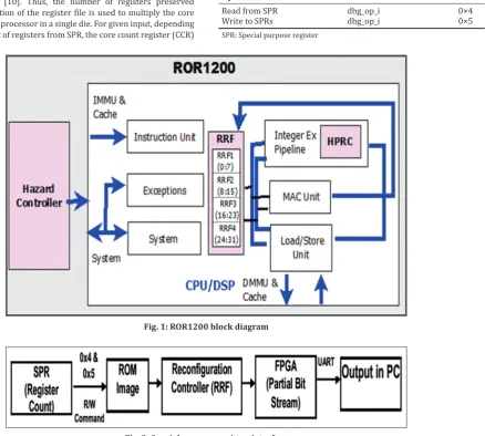
OR1200 is a 5 stage pipeline. Implements 32-bit instruction set with a processor conforming to the Harvard micro - architecture (separate memory unit for Instruction and Data). Reconfigurable computing affords high flexibility which permits designers to implement any new operation to the existing structure. The ROR1200 (Reconfigurable OpenRISC1200) is soft-core with dynamic reconfigurable units such as high-performance reconfigurable computing (HPRC) and reconfigurable register file (RRF) as shown in Fig. 1.
The register utilization is reduced in the ROR1200 by identifying the number of registers required for a specific application. ROR1200 reconfiguration explores compiler techniques to identify the number of registers essential for an application. The ROR1200 development interface is used to transfer the number of registers via commands © 2017 The Authors. Published by Innovare Academic Sciences Pvt Ltd. This is an open access article under the CC BY license (http://creativecommons. org/licenses/by/4. 0/) DOI: http://dx.doi.org/10.22159/ajpcr.2017.v10s1.19632
Full Proceeding Paper
School of Computing Science and Engineering, VIT University, Chennai, Tamil Nadu, India. 2Department of Electrical and Electronics
Engineering, Sri SaiRam Engineering College, Chennai, Tamil Nadu, India. Email: [email protected]
ABSTRACT
The prospective need of single instruction and multiple data (SIMD) applications like video and image processing in single system requires greater flexibility in computation to deliver high-quality real-time data. This paper performs an analysis of field programmable gate array
(FPGA)-based high performance reconfigurable open reduced instruction set computer 1200 (ROR) soft-core processor for SIMD. The ROR1200 ensures performance improvement by data level parallelism executing SIMD instruction simultaneously in high-performance reconfigurable computing (HPRC) at reduced resource utilization through reconfigurable register file with multiple core functionalities. This work aims at analyzing the functionality of the reconfigurable architecture, by illustrating the implementation of two different image processing operations such as image convolution and image quality improvement. The multiply-accumulate (MAC) unit of ROR1200 used to perform image convolution and execution unit with HPRC is used for image quality improvement. With parallel execution in multi-core, the proposed processor improves image quality by doubling the frame rate up to 60 fps (frames per second) with peak power consumption of 400 mWatt. Thus, the processor gives a significant computational cost of 12 m with a refresh rate of 60 Hz and 1.29 ns of MAC critical path delay. This FPGA-based processor becomes a feasible solution for portable embedded SIMD based applications which need high performance at reduced power consumptions.
images into instruction unit and the number of registers required will be communicated to the PC. Through batch files, RRF bit streams are burned in FPGA using Xilinx iMPACT. At the end of application execution, through UART the outputs are transferred to PC as shown in Fig. 2.
ROR1200 contains 32 registers each with 32-bit segregated into four blocks such as RRF1:RRF4. It also supports read and write operations through development interface. The register file is mapped through address ranging from 1024 to 1055.
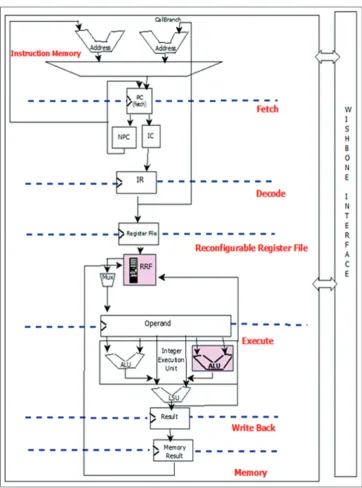
The internal design flow of ROR1200 is shown in Fig. 3. In this model, two zones are available like static and dynamic. Dynamic zones are reconfigurable region, whose partial reconfigurable bit streams were generated and placed in FPGA. Through internal configuration access port the internal HPRC (execution unit) is reconfigured in soft-core processor. Multiplying core functionality
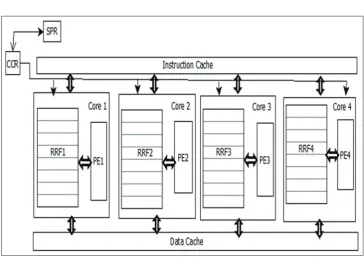
With registers the core functionality can be multiplied through C-slow retiming concepts [10]. Thus, the number of registers preserved during reconfiguration of the register file is used to multiply the core functionality of the processor in a single die. For given input, depending on the requirement of registers from SPR, the core count register (CCR)
all its operations very effectively considering their dependencies of data and flow of the program. The hardware component of those systems must be more flexible to handle different computational techniques efficiently without wasting the available hardware resources [11].
The two boarder ways to handle SIMD based system such as image and video processing systems are spatial level parallelism and data level parallelism [12]. For video processing applications, required performance level is achieved in processor architecture exploiting data-level parallelism [13]. In this work, data level parallelism is incorporated by creating a reconfigurable unit in integer execution units of the processor and resource utilization is handled through RRF.
Table 1: SPR operations and commands
Operation Command Value
Read from SPR dbg_op_i 0×4
Write to SPRs dbg_op_i 0×5
SPR: Special purpose register
Fig. 1: ROR1200 block diagram
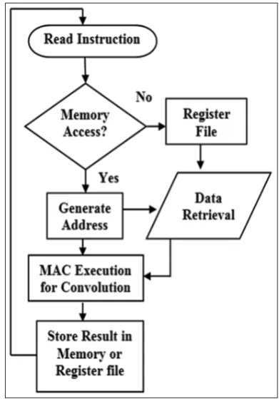
Image convolution using MAC
Image convolution is the process of performing dot operation (multiplication) of the image window with a finite impulse filter value represented in “(1).”
Convolution (x,y) = ∑(i,j)∈Region ((I(x+i), (y+j)).H(i,j)) (1)
Where I(x+i), (y+j) is an input image and H(i,j) is a kernel (filter). This image convolution helps to perform image smoothening, sharpening,
intensifying image, so on. Most of the SIMD-based applications like image and video processing need manipulation of 32-bit signed integer for efficient implementation of convolution operations. Hence, the MAC unit in the DSP of OR1200 is thus used to perform image convolution operation represented in equation 1 with fast Fourier transform computation. The MAC of OR1200 contains a multiplier cum accumulator unit integrated with an adder block supporting operation of 32×32 with resultant value of 48 bits stored in the accumulator. MAC is implemented in 5-stage pipelining technique Fig. 3: Reconfigurable register file access in ROR1200
To do hardware loops with the MAC`s, the 32-bit data have to be taken from the shared memories. The computed results can also be written to memory or to register RRF. The inputs of the data paths are 32-bit, but internally they are sign or zero extended (depending on the operation). Internally, all computations are 48-bit to provide a high precision of the result. The 48-bit results can be rounded, saturated, and truncated to get the 32-bit native length of the output [13].
The processor supports repeat instruction and a loop instruction. The repeat instruction takes two arguments as input, the number of instructions that should be repeated and the number of loops that should be performed. These results in only one repeat instruction that is as easy to use for repeating one instruction as it is to repeat multiple instructions and provide a hardware loop [13]. The data flow of the MAC is given in Fig. 5.
An image of 1024 px width is taken, in which each row of the image is split into 4 blocks of each holding 128 words. Each pixel is represented by 32-bit word. While executing each execution unit (Generic +HPRC) gets 4 px per row, which are stored consecutively in its data cache retrieved via register file. Each unit can retrieve its neighboring pixels in both directions (vertical and horizontal) directly without any network latency [15].
−
read 2M+n 1
M =
n (2)
The integer execution unit along with HPRC unit executes the same instruction simultaneously performing required row shift (left or right directions). Based, the MAC operations are needed to be performed as many times as blocks the image is split, in this case 4, to process completely a single image row. The MAC units are interfaced with a multiplexed bus macro for data transmission via bus macro controller. Based on the number of CCR, the MAC controller samples the input. Data representation in memory
The data representation of 3×3 convolution of 1024 px image is shown in Fig. 7 with mapping the registers for processing. This allows the processor to complete eight sets of 32-bit data operations per cycle when the SIMD pipeline is full.
MAC unit in each core performs an image convolution simultaneously to increase the performance of the processor.
The resultant output image after performing convolution images is given in Fig. 8a. It is the original image and Fig. 8b is smoothen image and Fig. 8c is sharpen image.
Image quality enhancement
In general, to display video without blurriness/jerkiness of the image frames, higher frame rate is required. For video applications, the frame rate can be increased by customizing the architecture with
Fig. 5: Data flow of multiply-accumulate
Fig. 6: Image convolution-matrix
Fig. 7: Data representation of image in one core Substituting values of input image and Kernel functions of Fig. 6
in equation 1. For 2D convolution:
Fig. 8: Image convolution, (a) original image, (b) smoothen image, (c) sharpen image
Fig. 9: Reconfigurable system design with high performance reconfigurable computing
c b
parallel execution of the input data set [14,16]. To perceive motion in the video, refreshing of the frames should take place very quickly. With 30 fps (frames per second), the monitor requires one 30th of frames, such as 33.3 m to display one frame as latency. This delay latency is halved when the frame rate doubles to 60 fps such as one sixtieth leading 16.6 m to display frames in monitor. The instruction fetch unit and instruction decode unit of the CPU are customized to process parallel executions of image data to increase the frame rate. Thus, data level parallelism through HPRC and integer unit with multiple core functionalities doubles the frame rate from 30 fps to 60 fps ensuring improved image quality of SIMD by increasing the processor performance by 50%.
Fig. 9 describes the reconfigurable system design with HPRC unit executing parallel instruction with RRF in out-of-order execution. Processor implementation design flow
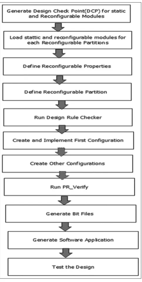
The design flow of the processor implementation is given in Fig. 10, where the Xilinx tool is used to generate design checkpoint for static and
reconfigurable modules. Then, the generated reconfigurable modules are loaded into its each partition. After defining the reconfigurable properties and partitions, run the design rule checker. Create and implement all the configurations to generate bit files and test the system design implemented on the board.
PERFORMANCE EVALUATION
To evaluate the performance, the framework of reconfigurable OR1200 is implemented in FPGA and its usability is tested with the real-time dataset. The performance result of implementation is given in Table 2.
Fig. 10: Implementation design flow
Fig. 11: Cost analysis
Fig. 12: Processing time analysis
Board implementation
The reconfigurable core is implemented in Xilinx Zynq FPGA to test the performance of the system. Using hardwired bus macros, the dynamic reconfigurable modules will be communicated with the static modules of the core [17]. The obtained results were compared with existing OR1200 with the proposed OR1200. The total number of slices available in targeted FPGA is 18796. The analysis result in an SIMD dataset is given in Table 3.
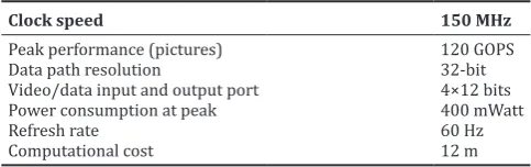
Look-up table (LUT) is used to provide synchronization with input data received from video camera to the output stream of the display monitor. The characteristics of implementation are given in Table 4.
Performance evaluation of SIMD
For 3×3 convolution, the MAC operation requires 9 cycles, whereas for 15×15 convolution it takes 12 clock cycles with frame size considered here is 1024 × 1024 px. Fig. 11 shows the cost analysis. Fig. 12 shows the processing time analysis and Fig. 13 shows the throughput analysis. Clock cycle: The first instruction takes five clock cycles for execution,
to perform the execution of N instructions it needs [5 + (N−1)] clock
cycles, if there are no branch instructions in the stream. CONCLUSION
Due to HPRC and RRF in soft-core processor, data-level parallelism is ensured using FPGA to support video processing applications at reduced power consumption. The multiple functional cores synthesized in 28 nm programmable logic Xilinx Zynq in a single die. The ROR1200 is a scalable and easily adaptable soft-core processor, providing increased throughput and performance with reduced resource utilization and power. Thus, the performance analysis of processor ensures doubled
frame rate from 30 fps to 60 fps with a significant computational cost of 12 m with a refresh rate of 60 Hz and 1.29 ns of MAC critical path delay. This FPGA-based processor becomes a feasible solution for portable embedded SIMD based applications which need high performance at reduced power consumptions.
1. Sinha P, Sinha A, Basu D. A novel architecture of a re-configurable
parallel DSP processor. Proceedings of the 3rd International IEEE
Northwest Workshop on Circuits and Systems, June 19-22, Quebec, Canada; 2005. p. 132-8.
2. Wittig RD, Chow P. One chip: An FPGA processor with reconfigurable logic. Proceedings IEEE Symposium on FPGAs for Custom Computing Machine; 1996. p. 67-74.
3. Stitt G, Vahid F. Energy advantages of microprocessor platforms with on-chip configurable logic. IEEE Des Test Comput 2002;19(6):36-43.
5. Alaraje N, DeGroat J, Jasani H. SoFPGA (System-on-FPGA) architecture: Performance analysis. IEEE International Conference on Electro, Information Technology. 2007. p. 551-6.
6. Haynes SD, Stone J, Cheung PY, Luk W. Video image processing with the sonic architecture. IEEE Comput 2000;33:50-7.
7. Horta EL, John WL, Taylor E, Parlour D. Dynamic hardware plugins in an FPGA with partial run-time reconfiguration. Design Automation Conference, USA. 2012. p. 343-8.
8. Kalte H. Dynamically reconfigurable system-on-programmable-chip. In: Euromicro Workshop on Parallel, Distributed and Network-based Processing. 2002. p. 235-42.
9. Ranganathan P, Adve S, Jouppi N. Performance of image and video processing with general-purpose processors and media ISA extensions.
To appear in the Proceedings of the 26th International Symposium on
computer Architecture. 2010. p. 78-82.
10. Nieto A, Vilarino DL, Brea VM. SIMD/MIMD dynamically-reconfigurable architecture for high-performance embedded vision
systems. IEEE 23rd International Conference on Application-Specific
Systems, Architectures and Processors. 2012. p. 96-101.
11. Kleihorst R. Camera Mote with a High-Performance Parallel Processor for Real-Time Frame-Based Video Processing. IEEE; 2007. p. 69-74. 12. Xilinx Soft Processors. Xilinx Inc. Available from: http://www.xilinx.
com/microblaze.
13. Kumar C, Azam MS. A multi-processing architecture for accelerating
Haar-based face detection on FPGA. IEEE 9th International Conference
on Industrial and Information Systems (ICIIS). 2014. p. 1-5.
14. Rana S, Mehra R. Design and simulation of RISC processor using hyper pipelining technique. IOSR J Mech Civil Eng IOSR JMCE 2014;9(3):49-57.
15. Perumall DU. An efficient reconfigurable image compression architecture. IEEE - ICSCN, MIT Campus, Anna University, Chennai, India. February 22-24, 2007. p. 265-9.
16. Diken E, O’Riordan MJ, Jordans R, Jozwiak L, Corporaal H. Mixed-length SIMD code generation for VLIW architectures with multiple native vector-widths. IEEE Conference: Application-specific Systems, Architectures and Processors (ASAP), Toronto; 2015. p. 181-8. 17. Kiefer G, Seider M, Schaeferling M. ParaNut - An open, scalable
and highly parallel processor architecture for FPGA-based system. Embedded World Conference, Nuremberg, Germany; 2015. p. 1-7.
Table 2: Performance result
Processor Application Cost (Number of cycles) Throughput (Mpx/s) Processing time (m)
ROR1200 3×3 convolution 0.876 170 1.8
15×15 convolution 0.458 90 3.6
OR1200 3×3 convolution 0.922 158 2.31
15×15 convolution 0.518 80 4.35
Table 3: ROR1200 versus OR1200 for SIMD Analyzing
parameter ROR1200 OR1200
Number of slices used 6390 9773
% of slices used 34 52
Minimum period 12.7 ns 14.1 ns
SIMD: Scottish index of multiple deprivation
Table 4: Characteristic features of FPGA
Clock speed 150 MHz
Peak performance (pictures) 120 GOPS
Data path resolution 32-bit
Video/data input and output port 4×12 bits
Power consumption at peak 400 mWatt
Refresh rate 60 Hz
Computational cost 12 m
FPGA: Field-programmable gate array
REFERENCES