R E S E A R C H
Open Access
Intensity feedback-based beam wandering
mitigation in free-space optical communication
using neural control technique
Arockia A Bazil Raj
1*, Arputha J Vijaya Selvi
2, Kumar D Durai
3and Raghavan S Singaravelu
4Abstract
Over the last two decades, free-space optical communication (FSOC) has become more and more interesting as an adjacent and/or alternative to radio frequency (RF) and optical fiber communications. The optical wave propagation in the FSOC channel is severely affected by atmospheric parameters, and it leads to the degradation of the data transmission quality and reliability. Among the various atmospheric effects, the beam wandering is the main cause of major power loss and cannot be solved without the incorporation of the beam centroid stabilization system. Therefore, designing a suitable opto-electronic assembly with a beam wandering mitigation system becomes significant to improve the performance of the FSOC system. A FSOC experimental setup is developed for the link range of 0.5 km in the college campus. A neural controller is designed for beam wandering mitigation. The neural controller processed the beam pointing (beam location) information obtained from an opto-electronic position detector (OPD) and then generated the necessary control outputs to the fast steering mirror (FSM) to steer the beam in the counter-direction to mitigate the beam wander at the receiver station. New design approach and architecture development for the implementation of the designed neural controller in the field-programmable gate array (FPGA) to mitigate the beam wandering are presented. The investigations on the performance of the neural controller in aiming a laser beam to be at a particular point on the detector plane are tested under dynamic disturbances generated at the transmitter in addition to the atmospheric effects through which the maximum correction capability of the developed neural controller is examined. Evidence of the suitability and the effectiveness of the proposed neural controller is evaluated in terms of beam centroid displacement, power spectral density (PSD), radial displacement on a 2D plane, effective scintillation index (ESI), Q-factor, and bit error rate (BER). The beam wandering range of−0.13 to +0.16 mm, maximum of 55 dB disturbance band attenuation with a frequency range of 0 Hz through 2 kHz, ESI of 0 to 0.15, Q-factor of 6, and BER of 6.45 × 10⁻⁹are achieved due to the incorporation of the developed neural controller in different real-world environmental conditions.
Keywords:Non-linearity; Intensity feedback; Neural controller; Beam wandering; Scintillation and bit error rate
1 Introduction
Recent and rapid progress in information and communica-tion technology has exceeded our expectacommunica-tions for meeting the requirements of multimedia society in the twenty-first century. Free-space optical communication (FSOC) is con-sidered to be one of the key technologies for realizing very high speed multigigabit per second (multi-Gb/s) large-capacity terrestrial and aerospace communications [1,2].
The FSOC system provides a line of sight (LoS), wireless and high-bandwidth communication between remote sites. The FSOC system offers many transmission advan-tages including freedom from electromagnetic interference (EMI) and license or tariffs, flexibility, ease in installment, no need to dig up roads, last-mile access, service acce-leration, metro network extensions, enterprise connectivity, fiber backup, backhaul, and high security [3,4]. In addition, a photonics-based approach is expected to bring such ultra-high data rate wireless technologies to potential users and to meet and explore real-world applications at the earliest opportunity as a technology driver [5]. However,
* Correspondence:[email protected] 1
Laser Communication Laboratory (LCL), Kings College of Engineering, Punalkulam, 613 303 Thanjavur, Tamil Nadu, India
Full list of author information is available at the end of the article
the propagating optical wave is influenced in the FSOC channel by random atmospheric changes (wind speed, temperature, relative humidity, and pressure) [6], thermal expansion, weak earthquakes, and typical high-rise build-ing sways which result in decreasbuild-ing the average received power, increasing the bit error rate (BER), and severely degrading the communication link quality/reliability [7-9]. These are all the general problems that require attenu-ation to be dealt with. The major effects due to the ran-dom fluctuations of the atmospheric turbulence are (i) optical scattering and observation (characterized by at-mospheric attenuation); (ii) random optical power fluc-tuation (characterized by scintillation index); (iii) beam wandering, i.e., beam surface global (temporal) tilt due to beam centroid displacement on the detector plane (characterized by effective scintillation index); and (iv) wavefront distortions, i.e., beam surface (spatial) local tilt (characterized by the Zernike polynomials) [10-12]. The conventional data coding and/or modulation tech-niques can be used to equalize/compromise the first two effects with respect to weather conditions at a given in-stant of time [13,14]. The third and fourth effects cannot be compromised without incorporating the adaptive op-tics elements [15,16]. During data transmission, the angle between the transmitter-receiver LoS and the transmitting beam axis must be kept within a fraction of the transmit-ting beamwidth which may be as small as a few microra-dians. The increase in the transmitting beam divergence angle/diameter is one way to maintain the link between the transmitter and receiver. It is clear that an overly wider beam will increase the required laser power, which increases the terminal cost and complexity. On the other hand, an overly narrow beam may result in a cutoff of the communication when there is building sway and/or beam wandering [2,3,7,8]. The existence of a perfect LoS and continuous beam alignment between the communicating optical antennas is one of the key requirements for a successful installation of an FSOC system. To ensure an uninterrupted data flow, auto-alignment transmitter and receiver modules are necessary [12,17,18]. The data loss due to weak scintillation effects can be recovered using various data coding techniques developed for wire- and fiber-based communication systems [13,14]. In contest, beam wandering and deep signal fading (wave-front distortions) represent unique and significantly more challenging problems, which cannot be resolved using con-ventional data coding techniques, and a major incentive for the incorporation of adaptive optics technology (beam wandering mitigation and wavefront corrections) into the FSOC architecture is an active prevention of long-term data loss [12,15,16]. The first and most important re-quirement for the successful installation of FSOC is beam steering (reduction of focal spot wander) that mitigates the beam wandering (temporal distortions) [1,16-18] which
is the research component and main contribution in this work.
Therefore, designing a suitable control system for beam auto-aligning, tracking, and positioning (ATP) to mitigate the beam wandering so as to significantly im-prove the beam stability on the receiver plane becomes significant. The complexities of a beam ATP controller design for the beam wandering mitigation process is in-creased due to inherent non-linearity and hysteresis of opto-electronic components involved in the beam steer-ing process, thereby maksteer-ing the control of a non-linear system non-trivial [19-21]. The Artificial Neural Network (ANN) is the most popular intelligent tool especially for non-linear function approximation and control applica-tions due to its high ability of learning from sample data and yielding better results to the new data [20-22]. A new design approach is introduced in this paper for the hardware implementation of a neural controller in a field-programmable gate array (FPGA) to operate the beam ATP process at a faster rate and also in parallel. The unipolar non-return to zero on-off keying-intensity modulation-direct detection (UNRZ-OOK-IM-DD) scheme is used for data transmission [23,24]. In order to inten-sively evaluate the performance improvement of FSOC due to the beam ATP control system, the time series plot of beam centroid displacement (wandering) on a 2D opto-electronic position detector (OPD) plane received signal power fluctuation and the demodulated data are continu-ously recorded and used to carry out on/off line analysis and compute various communication parameters. The effective scintillation index (ESI), i.e., scintillation due to beam wandering, is estimated by [4,11].
ESI¼<I2> = <I>2−1 ð1Þ
where I is the received irradiance and <…> is the
tem-poral mean (ensemble average) intensity of the optical beam at the receiver which is equal to a long time aver-age assuming the process to be ergodic and a photo-diode is a single point detector. The received data are continuously recorded in the real-time oscilloscope, and the data statistics are used to evaluate the link performance by estimating the signal to noise ratio (SNR) that includes the received signal power and system noise as [10,24]
SNR¼P2top−P2base=Xσ2topþXσ2base ð2Þ
wherePtopandPbaseare the means of most predominant
peaks of a histogram constructed for high (‘1’) and low
(‘0’) logic levels, respectively, and σtop and σbase are the
(‘0’) logic levels, respectively. The system metric Q-factor (linear) is calculated by [24]
Q¼ Ptop−Pbase
= σtopþσbase
ð3Þ
The theoretical BER is estimated using Equation 3 and complementary error function (erfc) as [10,24]
BER¼0:5erfcQ=pffiffiffi2 ð4Þ
Equations 1, 2, 3, and 4 are used to quantitatively analyze the FSOC data link performance improvements so as to understand and ensure the greatest contributions of the developed new ATP control system.
The rest of the paper is organized as follows:‘Section 2’ presents the backgrounds and related works,‘Section 3’ describes the experimental setup construction and beam spot position data processing,‘Section 4’ explains about the novel digital architecture designed to implement the neural controller and universal asynchronous receiver transmitter (UART) manager,‘Section 5’discusses the ex-perimental results and data analysis, and‘Section 6’draws some conclusions.
2 Background and related works
In the last few years, a lot of controller designs related to laser beam ATP have been remarkably carried out and can be found in literature. The publications/results closely related to our work are briefed in this section. Two optimization models are developed and simulated by Xian Liu for continuously adjusting the transmitter power, wavelength, telescope gain to mitigate the beam LoS deviations due to building sway, and atmospheric interference. The continuous adaptation of these param-eters is difficult in real-time implementation, and also, this approach increases terminal cost and complexity [3]. E. Ciaramella et al. have presented a dedicated elec-tronic control unit that effectively tracks the signal beam wandering caused by atmospheric turbulence and mech-anical vibrations in a wireless optical data link of 212 m between two buildings in Pisa, Italy. The tracking beam is coupled with the single-mode fiber (SMF). In this work, two separate optical beams, one for data transmis-sion and another for beam steering control (beacon beam), are used [4]. Hanling Wu et al. have described the disturbances (spatial coherence degradation) of the atmospheric turbulence effects in coupling the laser beam with the SMF. The incorporation of adaptive optics to mitigate these effects is addressed. The coupling efficiency is improved using the Zernike model adaptive optics and the results are numerically evaluated. Various assumptions related to the atmospheric strength are made and the re-sults are obtained for corrected polynomials in simulation [8]. Wei Liu et al. have presented the significance of beam
pointing in FSOC in terms of BER, pointing error prob-ability density function (PDF), and intensity displacement on a focal plane. The fast steering mirror (FSM) is used to correct the displacement error using the parallel
con-troller developed in FPGA. The minimum BER of 10−9
is achieved. The experiment is conducted in an indoor laboratory setup consisting of a controlled (man-made) turbulence simulation box. The digital signal processor (DSP) is jointly used with FPGA to generate the beam steering control signal [9]. F. Gago et al. have explained the tip-tilt mirror control based on the FPGA technology for adaptive optics system and reported that the FPGA is the best viable platform for the control process when a huge amount of parallel processing is needed. The experi-ment is conducted with integer and floating point calcula-tions. The results are presented and analyzed. ChipScope tools are used to avail the auxiliary modules in the FPGA. The entire control setup is assembled on the optical breadboard inside the laboratory and the experiment is conducted [12]. Digital architectures developed in the FPGA for optical wavefront correction are described by K. Kepa et al. The design of the low-cost adaptive optics control system architecture is explained and the results are presented and analyzed. Mostly, a lookup table (LUT)-based design is followed, and experimentation is carried out with some test pattern in the laboratory environ-ment [15].
The backpropagation learning algorithm is used and the neural controller is implemented in the FPGA. The ex-perimental results are investigated [22]. M.R. Suite et al. have explained the way of installing the FSM and OPD to correct the focal spot position fluctuation and thus reduce the power loss. The experiment is carried out across the bay (20-mile round-trip) at the Chesapeake Bay Detachment (CBD) of the Naval Research Laboratory (NRL). The calibration results of the OPD is given and the experimental results with and without active correction are explained. The experiment is conducted with the un-modulated optical beam, and only the performance im-provement of the beam stability on the detector plane was studied [25]. Thus, designing an intelligent controller to resolve the non-linear and hysteresis behavior of the opto-electronic devices and building a low-power and compact hardware controller to generate a beam steering control signal by processing the beam position information be-come significant. Further, incorporating the developed control system in real-world open atmospheric FSOC data link and evaluating its greatest contribution by measuring and analyzing the typical communication pa-rameters are also essential.
3 FSOC experimental test-bed configuration and control strategy description
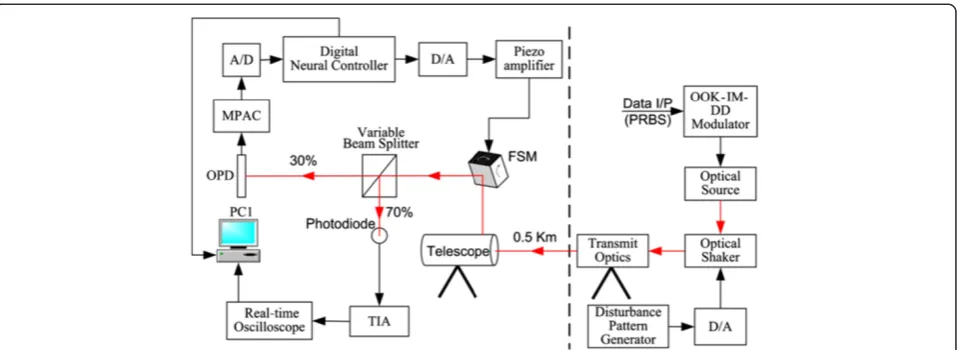
The FSOC experimental test-bed (transmitter and receiver) as shown in Figure 1 is developed for the data link range of 0.5 km at an altitude of 15.25 m with the necessary opto-electronic components. The schematic diagram of the experimental setup is shown in Figure 2 that consists of a modulatable Beta-Tx optical source, optical shaker, data and disturbance sequence generator circuit (in FPGA), digital to analog converter (D/A), and transmitting optics at the transmitter. The receiver consists of a telescope, FSM, variable beam splitter, OPD, analog to digital con-verter (A/D), and neural controller (in FPGA). All the opto-electronic devices are mounted on the vibration-damped optical breadboards [16,19]. A serial pseudoran-dom binary sequence (PRBS) generator circuit of 210-1 is
developed in the FPGA, and its bit stream output is given to the optical modulator at the asynchronous transfer mode (ATM) rate of 155 Mbps. A widely used UNRZ-OOK-IM-DD scheme, with a UNRZ signal of 0 V (low) for logic‘0’and 3.3 V (high) for logic‘1’, is used to directly modulate the optical signal [4,7,9,10,23]. The modulated light is made to fall on the optical shaker and gets reflected towards the transmitting optics. The trans-mitting optics increases the beam diameter from 3 mm (i/p beam) to 9 mm (o/p beam), and the expanded beam is transmitted to the receiver through the atmospheric tur-bulent optical channel. An arbitrary disturbance sequence (12-bit resolution) generator circuit is also developed in the FPGA at the transmitter, and its corresponding analog voltage is given to the optical shaker on which the Pure Reflection Mirror (PRM) is mounted and it acts as the secondary possible source of jitter. The OPD and PEAs are the key devices that facilitate fast and precise beam steering to mitigate the beam wandering in the FSOC sys-tem. According to the influence level of the local atmos-phere on the propagating optical wave, steering process requirements (optical feedback sensor, steering device, type/number of actuator, steering resolution, steering mir-ror aperture, control voltage, etc.) are chosen. The device identification, steady-state performance, and calibration analysis can be seen in our previous publication [19].
The telescope captures all the optical power and reflects to fall on the FSM. The FSM consists of a three-terminal PEA-based moving platform on which the beam steering mirror is mounted. The incident laser beam of the FSM gets reflected to the variable beam splitter that splits the incident light into two beams: reflecting beam and propa-gating beam.
The reflected beam is made to fall on the optical de-tector (photodiode) used for communication purposes. The photodiode generates a voltage related by a linear function with a negative slope to the intensity of light [16]. The propagating beam (passing through the beam splitter) is made to fall on the OPD. The OPD is con-structed with four separate identical silicon photodiodes
denoted by A, B, C, and D and arranged in a quad-rant geometry [19,25]. The output voltages of the OPD (VA,VB,VC, and VD) are given to the mono-pulse
arith-metic circuit (MPAC). The MPAC is constructed using operational amplifiers for accomplishing the addition and subtraction of the signal as given in Equations 5 and 6.
The beam spot (centroid) displacement errors VEx and
VEy along the x and y channels (2D plane) of the OPD
are measured as the relative output voltage changes by [19,25]
VEx¼fðVAþVCÞ−ðVBþVDÞg;
VEy¼fðVAþVBÞ−ðVCþVDÞg
ð5Þ
The reference signalVRefis measured by the algebraic
sum of all the signals from the quadrants of the OPD [19,25] as in Equation 6.
VRef ¼ðVAþVBþVCþVDÞ ð6Þ
The outputs of Equations 5 and 6 vary from −10
to +10 V and from 0 to +10 V, respectively. These signals are applied to the 12-bit parallel data-fetching A/D (AD1674 converter core) through an eight-channel analog multiplexer (ADG509A) circuit. The digitized outputs are given to the controllers via a very high density cable inter-connect (VHDCI). The information about the beam pos-ition (displacement) on the OPD (i.e., beam wandering data) are the key inputs to beam wander mitigating control system and are acquired continuously from the intensity feedback signal as shown in Figure 2. The important statistical values related to the beam displace-ment on the OPD are estimated using the following equations.
Azimuth and elevation distance are measured in mm by
xdist¼−2ðVEx=VRefÞ; ydist¼ þ2 VEy=VRef
ð7Þ
Radial distance is measured in mm by
γ¼ ffiffiffiffiffiffiffiffiffiffiffiffiffiffiffiffiffiffiffiffiffiffiffiffiffiffiffiffiffiffiffiffiffiðxdistÞ2þðydistÞ 2 q
ð8Þ
The feasible ranges of error and control parameters are taken from the manufacturer limitations. The PEA exhibits inherent non-linearities such as creep and hys-teresis [19-21,26]. The zero-friction piezo drives and flexure guidance allow sub-nanometer resolution and sub-microradian angular resolution. The hysteresis char-acteristics and step response of PEAs are generally non-linear and usually unknown [20,26]. This non-non-linear behavior limits system performance via undesirable oscillations and instability. The non-linear hysteresis behavior of PEAs is tested, and the mere inspection gives that the steering goes to the saturation, inverse and dislocated effect, and non-linear and distinctly asymmetric response [19]. The complexity in control of beam steering arises due to their geometrical configur-ation, the physical phenomena present in the PEA opera-tions, and other variables involved in its operation. The non-linear static input-output mapping of the system is not one-to-one [16]. Therefore, it is difficult to operate at an accurate trajectory using conventional controllers and a feed-forward neural network is put forward to resolve it [19-21]. Further, the conventional controllers could not be sufficient and the neural controller can be used for im-proving non-linear input-output mapping through which the beam wandering is mitigated and is the main contri-bution in this paper. The beam spot displacement error values are rescaled to lie within a range of−1 to +1. The
rescaling (normalization) is accomplished by the linear interpolation formula given in Equation 9.
σEx¼
displacement error on thexandypositions, respectively.
This normalization has the advantage of preserving exactly all relationships that do not introduce any bias. The error inputs and the corresponding control outputs are experimentally measured in the pilot survey using
the developed experimental setup shown in Figure2.
Al-though there are many parameters that affect the beam
steering process in beam stabilization, x and y
displace-ment errors contribute the greatest effect on the success of its operation. Advantageously, these parameters can easily be measured during the closed-loop feedback con-trol for beam steering operation with no additional cost
and time [27]. These parameters are considered as the
principal components in this work since they moreover directly affect beam stability and link quality. The neural controller output data (12-bit resolution) are converted to an analog signal using D/A and given to the FSM assembly through the piezo amplifier in a closed-loop feedback control. The beam position information, con-troller performance, demodulated data, and the quality metrics of data link are continuously monitored using the real-time oscilloscope and PC1.
4 Hardware architecture design and implementation of the neural controller
For on-chip training, the hardware platform suffers sev-eral disadvantages such as achieving high data precision, high hardware cost of calculations, development time, and flexibility of the platform as compared to the soft-ware [28-30]. At present, most of the neural controllers are simulated by software programs and implemented in a hardware platform due to the involvement of more computations and complicated arithmetic calculations in neuro-controller design. The FPGA or application-specific integrated circuit (ASIC) fabrication technology is more popularly being used due to the advantages of low power, compactness, huge amount of pipelined parallel data processing, and high speed computations [28,30]. Therefore, the neural controller weights and bias values are obtained from the MATLAB environment as a starting point for hardware implementation. The number of hid-den layers and neurons is determined through a trial and error method in order to accommodate the converged error within the goal. The neural network training algo-rithm, behavior of learning function, and development of
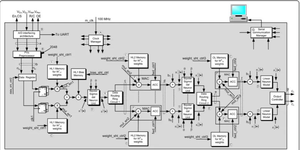
the neural controller can be seen in our previous publica-tion [19]. The 2-12-9-2 (2 neurons in the input layer (IL), 12 neurons in first hidden layer (HL1), 9 neurons in sec-ond hidden layer (HL2), and 2 neurons in the output layer (OL)) is the structure of the developed neural controller as shown in Figure 3. The fundamental mathematical equations related to the feed-forward multilayer percep-tron design with backpropagation learning algorithm can be found in section III of [22].
One of the trained patterns of the neuro-controller network structure is shown in Figure 3. A novel pipe-lined parallel architecture is developed in Xilinx FPGA and the neural controller is implemented. The ability of FPGA to perform massive parallel processing increases the obtainable control loop frequency, reduces the com-putational latency in the control system [15,22], makes the controller stand-alone, and operates at high speed [28]. The FPGA gives great flexibility in prototyping, designing, and developing complex hardware high gate density and many features necessary for neural controller implementation. The mixed design environment, very high speed integrated circuit hardware description language (VHDL) and Xilinx system generator, is used together since it simplifies the development of the neural con-troller and it is possible to model and simulate a digital system from a high level of abstraction module designs [31].
The global block diagram of intact digital architecture developed inside the FPGA is shown in Figure 4, and it consists of various main data processors and control en-gines. All the units/modules are developed to operate in parallel with the controlled data and command flow. The finite-state machine engine control information pro-vides a command signal that coordinates and executes various operations in the data processor section in order to accomplish the desired data processing task. The digital circuits act as the controller that provides a time sequence of signals for initiating the operations in the data path and also determine the next state of the control sub-system.
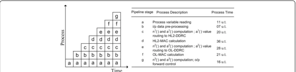
A pipelined parallel architecture is built for accom-plishing the necessary computations as per the neural controller algorithms. The pipeline level and the sched-ules of neural controller computation process flow are given in Figure 5, and the pipeline stages are marked by lowercase letters (a, b, c,…, g) in Figure 4. As can be seen in Figure 5, the operations are being performed at every moment. The feed-forward data flow is controlled by the pipeline stage control signal.
The developed novel architecture is divided into seven main blocks which are marked by uppercase letters (A,
B, C,…, G) in Figure 4, namely A) clock manager unit,
unit, and G) serial communication manager, and are described in the following sub-sections:
4.1 Clock manager unit (A)
The on-board clock frequency ‘m_clk’ in the FPGA
de-velopment board is 100 MHz. To achieve the required frequencies, the new clock signals have been synthesized by means of a digital clock manager (DCM) provided by
the FPGA. The block diagram of the clock manager module is shown in Figure 6a. The DCM output is given to the (i) internal shift controller, (ii) internal process controller, and (iii) enable signal generator. In these modules, starting from the DCM output, the required enable signals, shift control clocks, process control sig-nals, command sigsig-nals, data forward sigsig-nals, and baud rate clock etc. have been generated at the specified
Figure 3Trained pattern of the neural network.Typical backpropagation of the neural network pattern coded with weights and bias values for stand-alone linear time-invariant (LTI) controller.
synchronized frequencies for globally controlled data flow and operations.
4.2 Signal digitization and data pre-processing unit (B) This unit consists of two circuits, namely (i) A/D inter-facing architecture and (ii) process variables (PVs) pre-processor. The A/D interfacing circuit is developed in the FPGA as shown in Figure 6b. The data required to enable (En) the analog multiplexer (MSB of MUX o/p) and Channel Select (CS) address (MSB-1: LSB of MUX o/p) are stored in the channel control register. The MUX routes the content of the channel control register in accordance with the present state of the ‘ch_sel_ctrl’ finite-state machine controller. The 12-bit output of A/D corresponding to the selected channel is forced to avail-able at the input of the DMUX by asserting the Output
Enable (OE) control signal. The DMUX input is directed to the respective 12-bit wide register. The selective lines of the MUX and DMUX are synchronized for the proper operation with the finite-state machine. Once the content of all the registers are loaded, then the values are for-warded into the PVs pre-processor module. This action is
accomplished by the command ‘data_sht_ctrl1’ from
the finite-state machine. The PVs pre-processor performs the normalization operation as given in Equation 9, and the design flow graph is shown in Figure 6c. The radix-10 representation range of a 12-bit digitizer output is 0 through 4,095 with the center value of 2,048 for the 0-V input.
The VEx and VEy are compared with 2,048 (0 V) to
identify the direction of the beam displacement, i.e., left
or right on the x channel and above or below on the
Figure 5Example of pipelined process-timing diagram (brief) showing the computation process of neural controller with process description and time.
Figure 6Block diagram of the clock manager module. (a)Schematic diagram of the digital clock manager unit.(b)Eight-channel and 12-bit parallel out bidirectional (−10 to +10 V) A/D interfacing and data acquisition circuit.(c)Hardware design flow graph of the data normalization algorithm in PVs pre-processor unit. Error signalsVExandVEyvariations are normalized with respect toVRef. An error signal of 0 V is equal to 800
y channel, and the sign bit ‘s’ is concatenated with the values ofVExandVEywith respect to the decision of the
comparator. To measure the inner scale magnitude of the beam displacement on the OPD, 2,048 is subtracted from the values ofVEx,VEy, andVRefand then the results
ofVExandVEyare divided by the result ofVRef, so that
theVExandVEyare normalized with respect to theVRef.
The normalized values of PVs σEx and σEy are loaded
into the data register and forwarded to the D-FFs array through the data register. The content loading and forwarding to/from data register are performed by the control signal‘data_sht_ctrl2’as shown in Figure 4. The
Q(t +1) =Q(t) for the rising edge of the ‘clk1’and this state is maintained till accomplishing inputs and synaptic weight multiplications followed by the addition of bias for the HL1 computations in a single-precision data for-mat [32]. The next rising edge of the ‘clk1’ is applied to read and forward the subsequent inputs for HL1 computations.
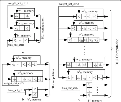
4.3 Weight and bias memory management circuit (C) The synaptic weights and bias values in the single-precision floating point format are stored in the RAM:
W1
x1, W1x2, and b1x for HL1; W21x, W22x, W23x,…W28x, W29x,
and b2x for HL2; and W31x, W32x, and b3x for OL. The
organization of weight and bias memory is shown in Figure 7, and the addresses are allocated based on the priority of data sequence forwarding for successive computations.
The RAM units are constructed as a circular data shift register, so that it forwards the chosen weight and bias values to the feed-back path as well as to the multiplier in the feed-forward path [30]. Three 12-element row vectors, nine 12-element row vectors with one 9-element column vector, and two 9-element row vectors with one 2-element column vector are the structure of the HL1, HL2, and OL memory, respectively. The input, synaptic weight, and bias value shifting are synchronized with the clock manager units that are controlled by the ‘weight_sht_ctrl1’ and ‘bias_sht_ctrl1’ signal for HL1, the ‘weight_sht_ctrl2’and ‘bias_sht_ctrl2’signal for HL2, and the ‘weight_sht_ctrl3’ and ‘bias_sht_ctrl3’ signal for OL. The weight and bias values are serially shifted to perform the input-weight multiplications, cumulative and bias addition operations to compute the net input of neuron‘n1(.)’in HL1 and the weight are serially and bias are paralleley shifted to perform the multiply and accumu-lation and bias addition operations to compute the neuron net inputs‘n21(.) to n29(.)’and ‘n31(.) and n32(.)’ in HL2 and
OL, respectively.
4.4 Neuron unit (D)
The neuron unit (activation function) is implemented to calculate the activation level of net input‘n’[28,33]. The
neurons in the HL1 and HL2 are bipolar sigmoidal acti-vation functions and in the OL are bipolar linear activa-tion funcactiva-tions. The bipolar sigmoidal activaactiva-tion funcactiva-tion is normally modeled by the hyperbolic tangent function [28,30,33] which cannot be easily implemented in the FPGA since it consists of infinite exponential series [29]. The drawback of using an alternative method of lookup table for bipolar sigmoidal activation function imple-mentation [30] is the need and utilization of a huge amount of hardware resources; therefore, it is imple-mented as a second-order non-linear function as in Equation 10 in FPGA, and various other methods of implementation of activation function can be found in literature [33].
where L and &−L are the upper and lower saturation
limits,nis net input to the neuron,βis the slope of the
model function, andθ is the gain of the model function.
The digital architecture of neuron implementation using the Xilinx system generator (Xilinx block sets) is shown
in Figure 8a. The net input ‘n’is multiplied by the gain
(θ), and the multiplier output is forwarded to another two processes that adds and subtracts to/from the slope (β). The results are given to the multiplexer which for-ward one of two inputs with respect to the selection
in-put (S1: 0 = first input, 1 = second input). The output of
the first multiplexer is multiplied by the net input ‘n’
and goes to the second multiplexer which forwards one of three inputs depending upon the selection input
(S2: 0 = first input, 1 = second input, 2 = third input). The
simulation results of real and second-order non-linear
bipolar activation functions for the input range of (−255,
255) are shown in Figure 8b, and the important
observa-tions are (i) the response of the second-order non-linear model precisely fits with the real model; (ii) the input range, slope, gain, and upper- and lower-limit parameters can be varied based on the application; and (iii) the possi-bility of Xilinx block set-based effective hardware imple-mentation. Only one neuron is implemented instead of 12 neurons in the HL1, and full activation-level computations are accomplished by the cyclic shifts of inputs, weight, and bias (W1x1, W1x2, andb1x) and the input and output of the neuron are denoted by‘n1(.)’and‘a1(.)’, respectively. In the HL2, 9 neurons are implemented and the input and output are denoted byn21(.),n22(.),…n29(.) anda21(.),a22(.),…
a2
9(.), respectively. The OL consists of 2 neurons and the
4.5 Data routing ring circuit (E)
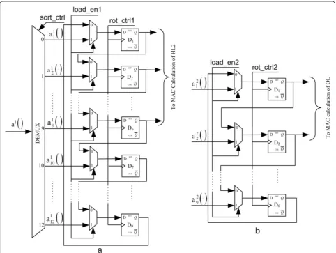
Two data routing ring circuits (DRRCs) are designed and used in such a way as to utilize the minimum amount of hardware resources to feed the data to the multiply-accumulation unit as a serial-in serial-out cir-cular shift register (SISOCSR) for the HL2 and OL con-figuration as shown in Figure 9a,b. The DRRC units are developed based on the methodology of neuron config-uration, i.e., one neuron or multiple neurons. Since one neuron is implemented in HL1, a 1 × 12 demultiplexer is used in the first DRRC to sort the input value into the corresponding second input of a 2 × 1 multiplexer, i.e.,
a1
(.) is demultiplexed to a11(.), a12(.), a13(.),…a112(.) as
shown in Figure 9a, and this sorting is accomplished by the command selection line ‘sort_ctrl’ signal. Initially, the selection line of a 1 × 2 multiplexer ‘load_en1’ is set
to ‘1’. Therefore, the sorted data are available at the input of the SISOCSR; otherwise, the 1 × 2 multiplexer output depends on the first input, i.e., the output of the previous register.
As soon as one set of sorting is over, the register clock ‘rot_ctrl1’ is applied and then the register outputs are available at the first input of 1 × 2 multiplexers. At this time, the‘load_en1’is set to‘0’, so that one circular shift is accomplished asa112(.), a11(.), a12(.), a13(.), a14(.), a15(.), a16
(.), a17(.), a18(.), a19(.), a110(.), and a111(.). These cyclic
rota-tions are continued for 12 subsequent clock inputs and then repeated with a new set of input data. The first nine register outputs are given in parallel to the HL2 multiply-accumulation computations. The outputs of the HL2 neurons a21(.), a22(.), a32(.), a24(.),…a29(.) are directly
given to the second input of the 1 × 2 multiplexer of OL
DRRC as shown in Figure 9b. The‘load_en2’is set to‘1’; therefore, the inputs are available at the input of the reg-isters. The register inputs are shifted to the next stage
when the clock ‘rot_ctrl2’ is applied and the status
becomes a29(.), a21(.), a22(.), a23(.),…a28(.), and at this time,
the‘load_en2’is set to‘0’. These cyclic rotations are con-tinued for 9 subsequent clock inputs and then repeated
with a new set of input data. The first two register outputs are given in parallel to the OL multiply-accumulation computations.
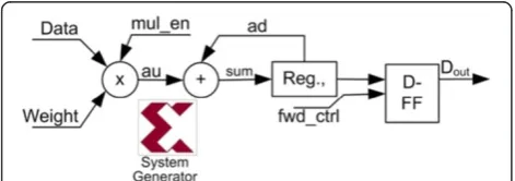
4.6 Multiply-accumulator unit (F)
The two main factors considered during the hardware implementation of Multiply-ACcumulator (MAC) units
Figure 8Digital architecture of neuron implementation using the Xilinx system generator. (a)Hardware design flow graph of the hyperbolic tangent sigmoidal (bipolar) activation function model as the second-order non-linear function and(b)plot of real and modeled neuron behaviors withσ=0.032,θ=1,β=255,n∈{−255,255}, andL= ±β/2.
are (i) need of reasonable precision and (ii) cost of more logic area associated with precision [30]. The single-precision (32-bit) floating point arithmetic standard is used for accomplishing the input and synaptic weight multiplications with bias additions and all the arithmetic operations [32]. The two modules of the MAC unit architecture are (i) multiplication and (ii) result accumu-lation. The design flow graph of the MAC circuit is shown in Figure 10. The nine MAC units for HL2 and the two MAC units for OL are developed for neuron in-putsn21(.) throughn29(.) andn31(.) andn32(.) computations.
The first MAC unit section multiplies the outputs of the first DRRC with the corresponding weights and is accu-mulated. The weight values and DRRC output shifting are controlled and synchronized by the internal shift
controller unit. The command ‘mul_en’ signal ensures
the availability of DRRC outputs and respective weight data and triggers the multiplication process. In accumu-lation, the multiplier output‘au’is added with the previ-ously accumulated value ‘ad’ and the result ‘sum’ is stored in a register for future accumulation. Once one MAC operation for one complete set of inputs is accom-plished, the final result is forwarded to the bias addition
in parallel for the rising edge of command ‘fwd-ctrl’
signal so that the final output, i.e., the inputs to the HL2 neurons n11(.) through n19(.) are ready. Similarly,
the second MAC unit section multiplies the outputs of the second DRRC with the corresponding weights, accumulates, and finally forwards to the bias addition in parallel, so that the OL neural inputs n31(.) and n32
(.) are ready. The OL neuron outputs are given to the D/A circuit.
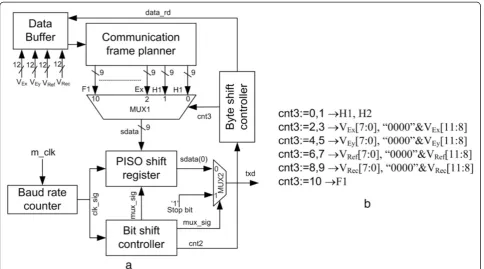
4.7 Serial communication manager (G)
The Universal Asynchronous Receiver Transmitter (UART) RS232 standard communication protocol is implemented as a separate digital architecture in the FPGA as shown in Figure 11a. The output of the MUX1 is forwarded to the parallel-in serial-out shift register (PISOSR) and sends 1 bit at a time to the MUX2 for the rising edge of the ‘clk_sig’signal. The output of the mux2‘txd’is‘sdata(0)’, i.e., LSB of PISOSR, when the selection line‘mux_sig’is set to‘0’; otherwise, the stop bit‘1’. The baud rate counter
generates the bit transmission clock, i.e., baud rate
clock ‘clk_sig’ at the rate of 9,600 from the master
clock ‘m_clk’signal.
The transmission of the measurement (M/m) data bit at the PISOSR and the stop bit are controlled by the bit shift controller in accordance with the ‘clk_sig’. Further, the bit shift controller conveys the status of the frame transmission to the byte shift controller using‘cnt2’that switches the selection line of MUX1‘cnt3’to choose the next channel (frame). Once all the frames of M/m data corresponding to one sampling cycle are transferred, then the byte shift controller enables the data buffer to
read the new set of M/m data by the command‘data_rd’
and continues. In order to avoid the occurrence of com-munication conflict among the frames, two header (H1 and H2) frames are transferred followed by the M/m data frames and one footer (F1) frame for the appropriate coordination among the data, so that a total of 11 frames need to be transferred for every data acquisition cycle as shown in Figure 11b. A computer (PC1) is used to log all the M/m data to perform the on/off line computations related to the experimental data analysis.
5 Experimental results and data analysis
The developed neural controller is installed at the FSOC receiver experimental setup as an observer-based control for beam stabilization. The beam wandering mitigation experiment using the developed neural controller is con-ducted in different local weather conditions (monsoon, rainy, winter, pre-summer, and summer) in a period of 1 year. A highly accurate weather station is built [6] and used to continuously measure the local weather changes in diurnal periods. The measurements corresponding to the weather changes are stored in the data-logging com-puter. The results presented below are corresponding to the winter session (15 December 2013 - Sunday). In this season, the weather parameter variations from 1.5 to 5.1 ms−1with the standard deviation (Std) of 0.97 ms−1 for wind speed (Ws), 23°C to 31°C with the Std of 2.65°C for temperature (T), 52% to 94% with the Std of 13% for relative humidity (RH), and 1 to 4 km with the Std of 0.87 km for visibility (V) are observed. The Std of T and RH are high while those of Ws and V are low. The different conditions of the atmosphere observed on 15 December 2013 (Sunday) are hazy, with scattered clouds, misty, foggy, and partially cloudy. The disturbances are in-troduced in the beam propagation angle for the frequency range of 0 to 2 kHz at the transmitter in addition to the turbulent channel effects to validate the maximum cap-ability of the developed closed-loop neural-control system. The performances of the developed neural controller are intensively investigated in a closed-loop control configur-ation. Some of the important data experimentally acquired in real time are presented, and from them, the potential
and feasibility of the proposed neural controller are discussed. The outstanding performance of the neural controller in mitigating the beam wandering and redu-cing the received optical signal fluctuation is analyzed. The significance of the proposed controlling scheme in improving the reliability of the FSOC data link is evalu-ated, and the results are presented in this section.
5.1 Performance study of closed-loop experiment with intensity feedback control
The maximum performance of the controller could not be arrived at in an open-loop control configuration since it depends on the following: (i) accuracy of the estima-tion of the posiestima-tion errors using the OPD, (ii) long-term behavior of opto-electronic components, (iii) greater number of PEA motion cycles, (iv) surpassed magnitude and phase response (sensitivity) of the FSM, (v) achiev-able neural controller performance in the LTI control scheme, (vi) sensor noise, and (vii) initial LoS alignment. Therefore, the intensity feedback (as observer)-based closed-loop control configuration becomes significant. In the identified system considered in this work, the
optimum values are Cx*=0.2157 V and Cy*=−0.1634 V
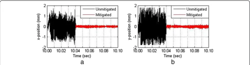
and these two values are very important in all the exper-iments. As a direct consequence of the beam wandering mitigation (disturbance rejection) in each channel, the ensemble average value of the position errors are signifi-cantly closer to (0,0)mm. The test experiments to analyze
the improvements due to the neural controller in the closed-loop control configuration to the disturbances are conducted, and samples of the results are shown in Figure 12. It can be seen that the greater perform-ance improvements are attained once the neural controller is turned on.
The obtained min-max values of beam centroid
wander-ing in the no-control condition are −1.73 to +1.71 mm,
whereas in the control condition, the values were−0.13
to +0.16 mm for both channels. The statistical results show that the neural controller in a closed loop generates the accurate control signal as required to mitigate the beam wandering.
The power spectral density (PSD) is computed for the time series data to analyze the disturbance rejection as the function of frequency and shown in Figure 13. The
disturbance to the x channel has a spectrum-wide
low-frequency content in the range 0 through 2 kHz with two narrow bands approximately at 0.48 and 1.12 kHz. The correction input to the FSM has a frequency of 2 kHz. The PSD results show that the proposed control scheme is capable of rejecting disturbances in the range 0 through 2 kHz. The PSD greatly demonstrates that the
disturbance band is attenuated in the x channel by a
maximum of 45 dB as in Figure 13. The PSD of the spot motion indicates that most of the frequency content fall in the range of 0.45 to 0.85 kHz. A similar behavior is re-ported for theychannel. In theychannel, the disturbance
band is attenuated by a maximum of 55 dB approximately. The disturbance given to both channels has a spectrum composed of narrow band disturbances. Almost the same observations are commanded for a longer period in differ-ent weather conditions; the disturbance at the frequency range 0 through 2 kHz had been effectively rejected. Fur-ther, the results show that the neural controller is capable of significantly attenuating the disturbance affecting both channels. In this case, what is interesting to notice is that the overlapping frequency bands are noticeably attenuated, however, not as much as in the cases in which the frequency bands do not overlap due to cross interference between both channels as commented in literature [16,21].
5.2 Analysis of beam spot auto-alignment and reduction of wandering
Optical beam angular deflections along the propagation path wander the beam randomly out off the LoS be-tween the optical source and detector. The instantan-eous center of the beam, i.e., the point of maximum intensity, is randomly moving on the detector plane. The performance improvement in beam stabilization through the beam steering control system is tested in controller tuned on and tuned off conditions. The beam centroid
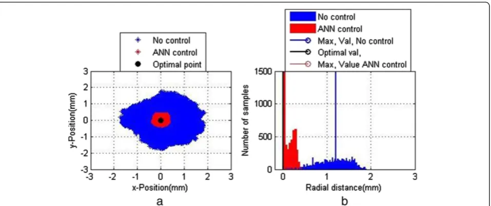
coordination on the 2D plane of the OPD is estimated using Equation 7, and a portion of data is shown in Figure 14a: with beam steering off (blue), beam steering on (red), and optimal value (black). The following are the interesting observations from Figure 14a in no control: (i) beam centroid wanders in almost all the areas of the OPD plane, (ii) centroid movements are highly random, (iii) sometimes the centroid goes out off the communication detector plane, i.e., the communication is disconnected, and (iv) the centroid shows a wide range of power fluctua-tions at the communication detector.
In the control are the following: (i) centroid movements are controlled and always around the optimal point, (ii) a very narrow range of power fluctuation is seen, and (iii) the maximum intensity of the beam (Gaussian beam) is concentrated at the center of the communication detector. The radial distance of the beam centroid on the OPD is calculated with respect to (0,0)mm using Equation 8, and the corresponding histogram plot is shown in Figure 14b: in no control (blue), in control (red), and optimal value (black) which evidences that the beam steering control system mitigates the beam wandering and stabilizes the beam almost at the center of the communication detector. The received signal magnitude is significantly improved and close to the optimal magnitudes in the presence of beam steering control, increases the reliability of the FSOC link, and maintains the stable SNR to decrease the BER. The average received signal magnitude is 0.0172 V for the 0-V (logic ‘0’) input due to sensors and circuit noise. The radial displacement distance is divided into six regions and denoted by the linguistic terms VS (0 to 0.5 mm), S (0.5 to 1 mm), M (1 to 1.5 mm), H (1.5 to 2 mm), VH (2 to 2.5 mm), and VVH (2.53 mm) where VS is very small, S is small, M is medium, H is high, VH is very high, and VVH is very very high.
5.3 Behavioral study of scintillation and communication signal quality metrics
The (0,0)V outputs from the OPD means that the beam centroid is positioned on the center of the photodiode
Figure 13Comparison of PSD of time series position data acquired with no control and control for thexchannel.
(communication detector) and its output is exactly mini-mum possible value, i.e., should coincide with the lower
bound of the photodiode outputVRec* =0.3162 V. In the
absence of sensor and circuit noise, the photodiode out-put difference at a given time (VRec(t) ~VRec*) measured
in volt is directly related to the atmospheric turbulence effects: scintillation and bam wandering. This beam wan-dering effect is mitigated using the developed beam steering system, so that the beam stability (maximum intensity) at a particular point on the photodiode is significantly improved. The power fluctuations of the received signal due to beam wandering are evaluated with and without the beam steering control system. The ensemble average of the optical power is used to esti-mate the ESI: power fluctuation due to beam centroid wandering, using Equation 1. The results corresponding to the 2,000 ensemble averages computed for control off and on conditions are shown in Figure 15a,b, respect-ively. ESI≤1 is corresponding to the VS and S and ESI >1 is corresponding to the M through VVH regions. For
lower values of ESI, the PDF distribution is nearly Gaussian centered about I0/<I> value of 1. As ESI
in-creases, the PDF is more skewed with a long tail towards the infinity and reduces peak intensity as a result of signal fading [1,4,10].
It is clearly reported from Figure 15 that the ESI fluc-tuates within broader variations (in the outer scale) from 0.014 to 1.86, i.e., 0.73% to 97.65% are seen when the steering is turned off. The variations in the inner scale with the min-max values of 0 and 0.15, i.e., 0% to 7.87%, are absorbed when the beam steering is turned on. These results exhibit the efficiency of the neural controller in steering the beam as required. Therefore, the neural controller in a closed loop improved the reliability of the FSOC data link. The ESI fluctuation, even with the beam steering turned on condition, reaches the maximum value of 0.15. This is due to a purely optical power fluctuation in the transmission path due to scintillation of the refract-ive index of the channel (Mie/Rayleigh scattering, absorp-tion and particle interacabsorp-tions with the optical beam, etc.)
Figure 14Laser beam spot centroid motion with and without beam steering control. (a)Beam wandering on a 2D-4Q plane with horizontal and vertical scales of real space.(b)Histogram of the beam centroid radial distance.
which could not be controlled by the steering system, but data coding and/or suitable modulation techniques devel-oped for modern digital communication system can be used to solve it significantly [2,4,10,13,14,23,24]. How-ever, this is the matter of separate research and out of the scope of this paper. As a direct consequence of the disturbance rejection in each channel, the average value of the photodiode output is significantly closer to the optimal value VRec*, despite the fact that {σEx(t), σEy(t)
and Cx(t), Cy(t)},∀t.
The beam is modulated by the PRBS data stream at the ATM rate of 155 Mbps. The quality of the data transmission in the FSOC link is measured in a daylong operation to study the stability and reliability of the communication system. The communication metrics such as signal power, Q-factor, SNR, and BER values are con-tinuously measured. All the measured values are stored in the data-logging computer. The Q-factor is measured as given in Equation 3 for different positions (S through VVH) of the beam centroid on the OPD; the correspond-ing theoretical BER is estimated uscorrespond-ing Equation 4 and shown in Figure 16. The Q-factor value linearly decreases and the BER increases with increasing the centroid radial displacement distance of the received beam. These re-sults exhibit the importance of the beam stabilization in the FSOC system and lead that the received beam must be stabilized regardless of its AoA. The beam steering control system turned on and turned off conditions are alternatively done in the 1-min time interval, and the dependence of the BER with the Q-factor is evaluated and the results are shown in Figure 17. The measured BER keeps close agreement with the theoretical BER. Note that the BER in Figure 17 is truncated to 6.46 × 10⁻⁹. The variation range of BER in no control is from 9.324 × 10⁻¹to 1.015 × 10⁻⁸and in control is from 6.4516 × 10⁻⁹ to 1 × 10⁻⁸which is less than 10−6. Once the control is on, the received beam is stabilized so that the value of the Q-factor is improved and hence the BER comes down to
below 10−8; otherwise, it falls in the upper regime.
Fur-thermore, the BER reaches greater than 10−6 even with
beam steering control in the beginning of measurement due to the pilot sequence synchronization scanning time, bit slip, and false detection in the real-time oscilloscope. As can be seen from Figure 17, a huge improvement com-pared to the no control experiments is demonstrated, the beam stability is improved, the outage probability is decreased, and the better BER is achieved without any forward error control (FEC) techniques.
The radial displacement distance values measured on 15 December 2013 for the diurnal period are subjected to generate the histogram plot to identify the most oc-curring sample values and their corresponding linguistic terms (S through VVH).
The most occurring sample values, linguistic terms, and minimum and maximum values of average BER are given in Table 1. The daylong measurements clearly demonstrate that the received beam centroid is retained within the VS region when the controller is turned on and the BER varies between 6.45 × 10⁻⁹and 1.04 × 10⁻⁸. The beam centroid wanders almost in all the regions when the controller is turned off, and the BER varies from 7.13 × 10⁻⁷to 1.34 × 10⁻¹. Almost the same results
Figure 16Experimental Q-factor and theoretical BER estimation against the beam centroid displacement on the OPD.
Figure 17BER as a function of Q-factor.Theoretical (black) and measured BER with the beam steering feedback turned off (blue) and on (red) alternatively for every 60-s time interval.
Table 1 Statistics of beam wandering and BER High frequency
sample (mm)
Radial distance linguistic
Average BER
Min Max
0.143 VS 6.45 × 10⁻⁹ 1.04 × 10⁻⁸
0.614 S 7.13 × 10⁻⁷ 7.81 × 10⁻⁵
1.235 M 8.51 × 10⁻⁵ 5.31 × 10⁻³
1.846 H 5.83 × 10⁻³ 1.41 × 10⁻²
2.314 VH 2.45 × 10⁻² 6.25 × 10⁻¹
have been reported in different weather conditions. Greater improvements in beam stabilization (coupling the power in the bucket to the communication detector) are achieved by the incorporation of the neural controller.
6 Conclusions
The significances of the received beam ATP system are reviewed. The most relevant literature survey results are briefed. The establishment of the 155-Mbps terrestrial FSOC data link for the range of 0.5 km at an altitude of 15.25 m with the necessary opto-electronic equipments is explained. The beam centroid displacement informa-tion is continuously obtained using the OPD and MPAC. The displacement and radial distance are estimated using the outputs of the MPAC. The optimal weights and bias (goal≤10−6) values of the designed neural con-troller structure of the 2-12-9-2 multilayer perceptron model are found in the MATLAB environment. The pilot survey experimental data are used to train and test the neural controller’s control signal prediction accuracy. A new design approach for the implementation of the neural controller in the FPGA is discussed. The architec-ture for implementing the UART RS232 standard com-munication protocol is developed as a separate digital architecture and used to transfer (store) the measure-ment/computational data to the computer (PC1) and to subsequently carry out on/off line data analysis.
The entire regions of the OPD are equally divided into six sub-regions, and the corresponding Q-factor and average BER values are measured and discussed. The FSOC performance improvements due to the beam wandering mitigation system are evaluated in control-ler turned off and on conditions. The values of the ESI are estimated and brought down to the controlled
range of 0 to 0.15. The beam wandering range of−0.13
to +0.16 mm, maximum of 55 dB disturbance band at-tenuation with a frequency range of 0 Hz through 2 kHz,
Q-factor of 6, and BER of 6.45 × 10⁻⁹are achieved due
to the incorporation of the developed neural controller in different real-world environmental conditions. The results presented in this paper are intended for setting up the FSOC transceiver. So, it is suggested that the use of the neural controller for fine steering applications is best instead of complex/complicated computational algorithms found in literature. This control scheme can also be used in various applications like beam stabili-zation, steering, focusing, beam spotting, beam coupling and real-time control system, etc. A new version of the neural controller for deformable mirror control is also being implemented in FPGA and will be finished in the near future.
Competing interests
The authors declare that they have no competing interests.
Author details 1
Laser Communication Laboratory (LCL), Kings College of Engineering, Punalkulam, 613 303 Thanjavur, Tamil Nadu, India.2Kings College of
Engineering, Punalkulam, 613 303 Thanjavur, Tamil Nadu, India.3Periyar Maniammai University, Vallam, 613 403 Thanjavur, Tamil Nadu, India.
4
Department of Electronics and Communication Engineering, National Institute of Technology, Tiruchirappalli 620 015, Tamil Nadu, India.
Received: 25 February 2014 Accepted: 23 September 2014 Published: 5 October 2014
References
1. PT Dat, CB Naila, P Liu, K Wakamori, M Matsumoto, K Tsukamoto, Next generation free space optics systems for ubiquitous communications. PIERS Online7(1), 75–80 (2011)
2. IB Djordjevic, Heterogeneous transparent optical networking based on coded OAM modulation. IEEE Photonics J.3(3), 531–537 (2011) 3. X Liu, Free-space optics optimization models for building sway and
atmospheric interference using variable wavelength. IEEE Trans. Commun. 57(2), 492–498 (2009)
4. E Ciaramella, Y Arimoto, G Contestabile, M Presi, A D’Errico, V Guarino, M Matsumoto, 1.28 terabit/s (32 x 40 gbit/s) WDM transmission system for free space optical communications. IEEE J Sel Areas Commun. 27(9), 1639–1645 (2009)
5. T Nagatsuma, Breakthroughs in photonics 2013: THz communications based on photonics. IEEE Photonics J. (2014). doi:10.1109/JPHOT.2014.2309643 6. AAB Raj, JAV Selvi, S Raghavan, Real-time measurement of meteorological parameters for estimating low-altitude atmospheric turbulence strength (Cn2).
IET Sci. Meas. Technol. (2014). doi:10.1049/iet-smt.2013.0236
7. N Kumar, AK Rana, Impact of various parameters on the performance of free space optics communication system. Optik124(22), 5774–5776 (2013) 8. H Wu, H Yan, X Li, Modal correction for fiber-coupling efficiency in
free-space optical communication systems through atmospheric turbulence. Optik121(19), 1789–1793 (2010)
9. W Liu, W Shi, J Cao, Y Lv, K Yao, S Wang, J Wang, X Chi, Bit error rate analysis with real-time pointing errors correction in free space optical communication systems. Optik125, 324–328 (2014)
10. ZGH Minh, S Rajbhandari, J Perez, M Ijaz, Performance analysis of ethernet/ fast-ethernet free space optical communications in a controlled weak turbulence condition. J. Lightw. Technol.30(13), 2188–2194 (2012) 11. Y Jiang, J Ma, L Tan, S Yu, W Du, Measurement of optical intensity fluctuation
over an 11.8 km turbulent path. Opt. Express16(10), 6963–6973 (2008) 12. F Gago, L Rodrfguez–Ramos, G Herrera, J Gigante, A Alonso, T Viera,
J Piqueras, JJ Diaz,Tip-Tilt Mirror Control Based on FPGA for an Adaptive Optics System. Proc. of the 3rd Southern Conference on Programmable Logic [Online] (Mar del Plata, Argentine, 2007), pp. 19–26
13. IB Djordjevic, Adaptive modulation and coding for free-space optical channels. J. Opt. Commun. Netw.2(5), 221–229 (2010)
14. T Schneider, A Wiatrek, S Preubler, M Grigat, R-P Braun, Link budget analysis for terahertz fixed wireless link. IEEE Trans. Terahertz Sci. Technol. 2(2), 250–256 (2012)
15. K Kepa, D Coburn, JC Dainty, F Morgan, High speed optical wavefront sensing with low cost FPGAs. Meas. Sci. Rev.8(4), 87–93 (2008) 16. NO Perez-Arancibia, JS Gibson, T Tsao, Observer-based intensity-feedback
control for laser beam pointing and tracking. IEEE Trans. Control Syst. Technol.20(1), 31–47 (2012)
17. C Si, Y Zhang, Beam wander of quantization beam in a non-Kolmogorov turbulent atmosphere. Optik124(12), 1175–1178 (2013)
18. F.D. Kashani, M. Reza Hedayati Rad, E. Kazemian, S.H. Golomohammady, Reliability analysis of an auto-tracked FSO link under adverse weather condition. Optik124(22), 5462–5467 (2013)
19. A Arockia Bazil Raj, J Arputha Vijaya Selvi, D Kumar, N Sivakumaran, Mitigation of beam fluctuation due to atmospheric turbulence and prediction of control quality using intelligent decision-making tools. Appl. Appl. Opt.53(15), 3796–3806 (2014)
20. W-F Xie, J Fu, H Yao, CY Su, Neural network-based adaptive control of piezoelectric actuators with unknown hysteresis. Int. J. Adaptive Control Signal Process.23, 30–54 (2009)
22. QN Le, JW Jeon, Neural-network-based low-speed-damping controller for stepper motor with an FPGA. IEEE Trans. Ind. Electron.
57(9), 3167–3180 (2010)
23. CW Chow, CH Yeh, YF Liu, PY Huang, Mitigation of optical background noise in light emitting diode (LED) optical wireless communication systems. IEEE Photonics J.5(1), 1–7 (2013). 7900307
24. H Hemmati,Near-Earth Laser Communication(CRC Press, Florida, 2009), pp. 59–96
25. MR Suite, HR Burris, CI Moore, MJ Vilcheck, R Mahon, C Jackson, MF Stell, MA Davis, WS Rabinovich, WJ Scharpf, AE Reed, GC Gilbreath, C Diego,ast Steering Mirror Implementation for Reduction of Focal-Spot Wander in a Long Distance Free-Space Communication Link. Diego, California (International Society for Optics and Photonics, San Diego, California, USA, 2004), pp. 439–446. 5160
26. G Guo Ying, LM Zhu, High-speed tracking control of piezoelectric actuators using an ellipse-based hysteresis model. Rev. Sci. Instrum.81(8), 1–9 (2010) 27. Y Lu, D Fan, Z Zhang, Theoretical and experimental determination of
bandwidth for a two-axis fast steering mirror. Optik124(16), 2443–2449 (2013) 28. E Monmasson, MN Cirstea, FPGA design methodology for industrial control
systems - a review. IEEE Trans. Ind. Electron.54(4), 1824–1842 (2007) 29. A Gomperts, A Ukil, F Zurfluh, Development and implementation of
parameterized FPGA-based general purpose neural networks for online applications. IEEE Trans. Ind. Informat.7(1), 78–89 (2011)
30. P Skoda, T Lipic, A Srp, B Medved Rogina, K Skala, F Vajda,Implementation Framework for Artificial Neural Networks on FPGA. Proc. of the 34th Int. Conv. MIPRO (Croatian Society, Opatija, 2011), pp. 274–278 31. A Tisan, M Cirstea, SOM neural network design - a new Simulink library
based approach targeting FPGA implementation. Math. Comput. Simul. 91, 134–149 (2013)
32. F Benrekia, M Attari, A floating point multiplier based FPGA synthesis for neural networks enhancement. Int. J. Eng. Sci. Technol.2(5), 1433–1440 (2010) 33. A Tisan, S Oniga, D Mic, A Buchman, Digital implementation of the sigmoid
function for FPGA circuits. ACTA Technica Napocensis50(2), 15–20 (2009)
doi:10.1186/1687-1499-2014-160
Cite this article as:Bazil Rajet al.:Intensity feedback-based beam wandering mitigation in free-space optical communication using neural control technique.EURASIP Journal on Wireless Communications and Networking20142014:160.
Submit your manuscript to a
journal and benefi t from:
7 Convenient online submission 7 Rigorous peer review
7 Immediate publication on acceptance 7 Open access: articles freely available online 7 High visibility within the fi eld
7 Retaining the copyright to your article