A Comparative Study of Low Power Area
Efficient Carry Select Adder
Nimisha A Deshmukh1, Prof AP Khandait 2, Prof Divya Meshram3
M. Tech Student (VLSI), Department of Electronics, Priyadarshini College of Engineering, Nagpur, India 1
Assistant Professor, Department of Electronics, Priyadarshini College of Engineering, Nagpur, India 2
Assistant Professor, Department of Electronics, Priyadarshini College of Engineering, Nagpur, India 3
ABSTRACT: Area, power and delay are the most design objectives of integrated circuits. There are many adders
present in VLSI design system for computational and data path processing unit, out of which carry select adder is fast and power efficient. However regular carry select adder is area consuming due to dual RCA structure. Therefore we use binary to excess one converter to overcome carry propagation delay problem and to achieve minimum area. Addition is the most common and often used arithmetic operation on microprocessor, digital signal processor, especially digital computers. Also, it serves as a building block for synthesis all other arithmetic operations. Therefore, regarding the efficient implementation of an arithmetic unit, the binary adder structures become a very critical hardware unit..
KEYWORDS: Carry select adder, Ripple carry adder, Binary to excess one converter, Modified carry select adder.
I. INTRODUCTION
The optimization of power area and speed are prime importance in VLSI industry. In order to achieve such a design specification high speed architectures are needed.As addition is the basic operation of all computer arithmetic operations, adders are one of the widely used components in digital integrated circuit design. An efficient adder design essentially improves the performance of processor and integrated circuits.There are many types of adder designs available (ripple carry adder, carry look ahead adder, carry save adder, carry skip adder) which have its own advantages and disadvantages. The Ripple carry Adder (RCA) exhibits the most compact design but slowest in speed because for an N-bit RCA, the delay is linearly proportional to N. Thus for large values of N the Ripple Carry Adder gives greater delay of all adders. To solve the carry propagation delay Carry select adder is developed which drastically reduces the area and delay to a great extent.
In digital adders, the speed of addition is limited by the time required to propagate a carry through the adder. The sum for each bit position in an elementary adder is generated sequentially only after the previous bit position has been summed and a carry propagated into the next position. The major speed limitation in any adder is in the production of carries and many authors have considered the addition problem. The carry select adder is used in many computational systems to moderate the problem of carry propagation delay by independently generating multiple carries and then select a carry to generate the sum.
The CSA is used in many computational systems to alleviate the problem of carry propagation delay by independent generating multiple carries and then select a carry to generate the sum. However, the CSA is not area efficient because it uses multiple pairs of Ripple carry adder(RCA) to generate partial sum and carry by considering carry input Cin=0 and Cin=l, then the final sum and carry are selected by the multiplexers (MUX).Hence, in this paper we have proposed a new technique of designing of carry select adder which will reduce area, delay and power.
II.CONVENTIONALCARRYSELECT ADDER
most significant bits (MSB’s) two k/bit adders. In MSB adders one adder assumes carry input as one for performing addition and another assumes carry input as zero. The carry out calculated from the last stage i.e. least significant bit stage is used to select the actual calculated values of output carry and sum. The selection is done by using a multiplexer. This technique of dividing adder in to stages increases the area utilization but addition operation fastens. The block diagram of conventional k bit adder is shown in figure1.Therefore in conventional carry select adder a pair of ripple carry adder is used, furthermore the ripple carry adder is designed by using cascaded connection of full adder as shown in figure 2
Figure 1: Block diagram of k-bit adder
Figure 2: Basic building block of CSA
A. Ripple Carry Adder:
An n-bit Ripple Carry Adder (RCA) is a simple cascading of n full adders. In this carry out of previous full adder becomes the input carry for the next full adder. As carry ripples from one full adder to the other, it traverses longest critical path and exhibits worst case delay. It calculates sum and carry according to the following equations.
Si = Ai xor Bi xor Ci
Ci+1 = Ai Bi + (Ai + Bi) Ci; where i = 0, 1… n-1 (1)
B. Full Adder:
A full adder adds binary numbers and accounts for values carried in as well as out. A one-bit full adder adds three one-bit numbers, often written as A, B, and Cin; Aand Bare the operands, and Cin is a bit carried in from the previous less significant stage. Thefull adder is usually a component in a cascade of adders, which add 8, 16, 32, etc. bit binary numbers. The circuit produces a two-bit output, output carry and sum.
Figure3: Block diagram of RCA
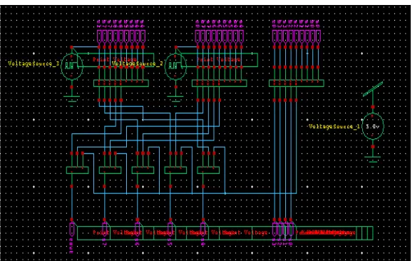
The schematic of ripple carry adder is designed on Tanner EDA tool which is shown in following figure 4
Figure4: Schematic diagram of ripple carryadder
III.PROPOSED SYSTEM
The regular CSA is not area efficient because it uses multiple pair of ripple carry adder hence area and carry propagation delay increases. Therefore to overcome the problem regular carry select adder is modified by using binary to excess- 1converter [3].This converter is used in place of ripple carry adder used for cin=1 in structure of regular carry select adder.
A. Binary to excess-1 converter:
Binary to Excess-1 Converter is a digital circuit that excess the value of the input to 1 means the value of input gets increased by 1 with the help of BEC-1.It is a digital circuit that uses 1 NOT gate, 2 AND gate and 3 XOR gates to perform the operation. Since Regular Carry Select Adder uses multiple RCAs to perform the addition operation of input bits individually for Cin=0 and Cin=1, then BEC-1 is used to perform the addition of input bits for Cin=1.The basic idea of this modified work is to use Binary to Excess-1 Converter (BEC) instead of RCA with Cin=1 in the regular CSLA to achieve lower area and power consumption with only a slight increase in the delay .Practically the circuit of BEC-1 is more compact and simpler as compared to RCA. The main advantage of this BEC-1 logic comes from the lesser number of logic gates than the n-bit Full Adder structure. The Boolean equation used for the operation of BEC are as follows
“&”:- and, “^” :- xor.
X0=~B0--- (1)
X1=B0^B1--- (2)
X2=B2^ (B0&B1) --- (3)
X3=B3^ (B0&B1&B2) --- (4)
B. Modified carry select adder:
In regular carry select adder ,two ripple carry adders are used for cin=0 and cin=1,due to which the overall area of circuit get increases as well as carry propagation delay also get increase. Hence to overcome this problem we have replace ripple carry adder for cin=1 by BEC [4]. The following figure 7 will show the modified carry select adder. Further to minimize the area we have designed the carry select adder with transmission gates [5]. Logic circuits can be constructed with the aid of transmission gates instead of traditional CMOS pull-up and pull-down networks. Such circuits can often be made more compact, which can be an important consideration in silicon implementations. The following figure shows the diagram of BEC and modified carry select adder using BEC.
Figure5: Block diagram of BEC
The schematic of BEC is shown in following figure 6.
Figure 6: Schematic of BEC
Figure 7: Modified carry select adder
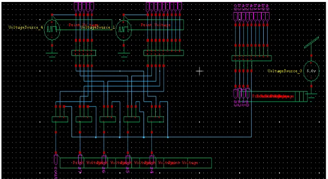
The modified carry select adder with transmission gate and BEC is desugned using Tanner EDA tool.Following figure 8 shows the schematic of adder.
Figure 8:Schematic of Modified CSA
IV.SIMULATION RESULTS
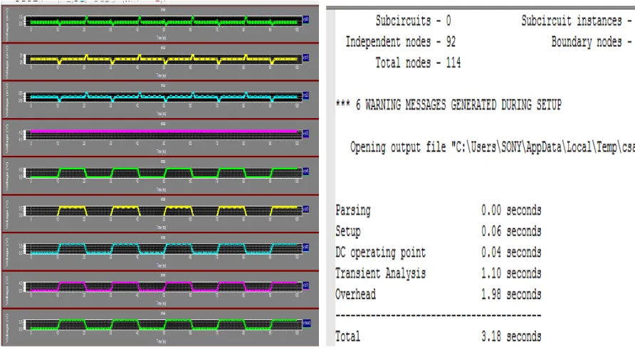
In this paper carry select adder and modified carry select adder are designed in s-edit of tanner tool and compared. We have used TSPICE simulation with 180 nm CMOS technology file using operating condition with frequency 50 MHz and supply voltage of 5V.The design is having less no of transistors as we have used transmission gate. The following results will show the simulation and timing analysis of both the adders.
Figure 9: Simulation of CSA using transmission gate Figure 10: Timing analysis of CSA
The following figure 11 and 12 gives specification of the modified carry select adder. Figure 11 is the simulation of modified carry select adder while figure 12 gives the timing analysis and total transistor count of the adder. The modified carry select adder is designed by transmission gate and binary to excess one converter.
Figure 10: Simulation Modified CSA with BEC Figure 12: Timing analysis of modified CSA
Table 1.Comparison between regular CSA Vs Modified CSA
Sr. No Carry select Adder Delay Transistor count
1 Regular carry select adder 3.18sec 246
2 Modified carry select adder 2.94 sec 218
V. CONCLUSION AND FUTURE WORK
In this paper regular carry select adder rand modified carry select adder which is designed by using binary to excess one converter are compared. The main aim was to optimize the area, delay and power of the system. Design of modified carry select adder is achieved by using transmission gate to optimize the area and binary to excess one converter. From the comparison table1, it is clear that proposed design has low area delay and power in comparison with regular CSA, thus problem occurred in regular CSA can be overcome by using this technique. The simulation results showed that the proposed system performs better with the binary to excess one converter than the regular one. We have used very small bit of adder of 8bit, as number of bits increase the complexity will increase. We can increase the number of bits and analyze the performance.
REFERENCES
1. B. Ram Kumar and Harish M Kittur, “Low-Power and Area-Efficient Carry Select Adder”, IEEE Transactions on Very Large Scale Integration (VLSI) Systems, Vol. 20, No. 2, February 2012.
2. K Allipeera, M.Tech Student & S Ahmed Basha, Assitant Professor, “An Efficient 64-Bit Carry Select Adder With Less Delay And Reduced Area Application”, International Journal of Engineering Research and Applications (IJERA) ISSN: 2248-9622 ,Vol. 2, Issue 5, September- October 2012.
3. M.Chithra1, G.Omkareswari,“128-bit Carry Select Adder Having Less Area And Delay”, International Journal of Advanced Research in Electrical, Electronics and Instrumentation Engineering Vol. 2, Issue 7, July 2013.
4. Bokam Krishnaveni1, P.Saroja,“An Efficient Implementation of Carry Select Adder with Low Power and Area Efficient Characteristics”, International Journal of Advanced Research in Computer and Communication Engineering Vol. 3, Issue 11, November 2014.
5. Rajwinder Kaur, Amit Grover, “Different Techniques used for Carry Select Adder - A Review”, International Journal of Computer Applications (0975 – 8887) Volume 116 – No. 3, April 2015.
6. Padma Devi, Ashima Girdher, Balwinder Singh, “Improved Carry Select Adder with Reduced Area and Low Power Consumption”, International Journal of Computer Applications (0975 – 8887) Volume 3 – No.4, June 2010.
7. Bedrij, O. J., (1962), “Carry-select adder,” IRE Trans. Electron. Comput. Pp.340–344.
8. M.Priyadharshini*, M.Thiruveni,” Performance Evaluation of Carry Select Adder-Review,” International Journal of Engineering Sciences & ResearchTechnology. ISSN: 2277-9655 November 2014.
9. Amol D. Rewatkar, Prof. Sumit. R. Vaidya, Prof. Rajashree. N. Mandavgane,”A Review Based on Performance of Carry Select Adder”, ISSN: 2393-994X Karpagam Journal Of Engineering Research (KJER) Volume No.: III, Special Issue on IEEE Sponsored International Conference on Innovations in Information, Embedded and Communication Systems (ICIIECS'15.
10. Ceiang, T. Y. and Hsiao, M. J., (Oct. 1998), “Carry-select adder using single ripple carry adder,” Electron. Lett. vol. 34, no. 22, pp. 2101– 2103.
11. Books:
1Mr.P Raja “DigitalElectronics”.