Design and implementation of Deadlock
Avoidance for On Chip Buses with Elastic
Buffer and Error Correction
Chithra Somasundaran, Sariga p s
M.Tech Scholar (VLSI &Embedded System), Dept. of ECE, IIET, M.G University, Kottayam, Kerala, India
Assistant Professor, Dept. of ECE, IIET, Nellikuzhy, Kerala, India
ABSTRACT: Advanced extensible interface protocol and open core protocol are protocols used for on chip communication it can support advanced transactions and it also improve communication efficiency. Out-of-order transactions are return responses in an order different from requested ones. Here we discuss a concept it can support out of order transactions. A graphical model used in the system known as bus status graph used to identify the occurrence of dead lock condition. According to this graphical model we propose a technique it can avoid this deadlock problem. And also using an error detection and correction method to avoid the mismatches in read and write operation between master and slave.
KEYWORDS: advanced extensible interface (AXI), On- chip buses , out of order transactions, tagged transactions, elastic buffer.
I. INTRODUCTION
Advanced high-performance bus and advanced peripheral bus [1] are the most architectures allowing only one master IP to access one slave IP at a time. Advanced communication protocols like advanced extensible interface (AXI) [1] and open core protocol (OCP) [1] can facilitate parallel communication . The communication protocols such as AXI and OCP support various transactions, like burst transactions, pipelined (outstanding) transactions, and out-of-order transactions [1], [2]. In these, out-of-out-of-order transactions plays a major key to improve system performance. Out-of-order transactions can execute more efficiently when a master IP, such as a processor, can handle out-Out-of-order returns as it allows a slave core such as a dynamic random-access memory controller to service requests in the order that is most convenient, rather than the order in which requests are sent by the master .
Bus deadlock problem happens when a set of IP cores are communicating through a bus system and their involved a circular wait-and-hold state that cannot be resolved. This problem will crash the bus system as none of the IP cores involved in the deadlock can continue its functions. In [5], bus deadlock problem of a system it allow the master to execute a process only if the master is granted to access all require slaves of the process and each master will hold slaves granted to it until all required slaves are granted to it. A bus deadlock occurs in case of a set of masters where master in a set of masters are holding a slave and waiting for another slave held by another master in the particular set.
II. RELATED WORKS
Data transactions are of two types they are single and burst transactions, where the single transaction is one which requests only one response whereas the burst transaction means that which requests multiple responses. Basic transactions can be pipelined or non-pipelined. In AXI, pipelined transactions are further divided into tagged as well as untagged ones, where untagged transactions executed in order, and the execution orders of the tagged ones are depend on the IDs they are tagged.
All untagged transactions must executed in order.
All tagged transactions having same tag ID must be executed in order.
No order restriction on the execution between tagged transaction and an untagged transaction.
Fig. 1. Bus models for (a) basic transactions, (b) pipelined transactions with buffers in the bus, and (c) pipelined transactions with buffers in the slave.
Fig. 1(a) shows a basic bus model which is compliant with AXI [1] protocols. Here, a complete bus transaction contains a request and a response phase. The basic non-pipelined transactions are executed in bus model of Fig. 1(a). With a single transaction, a master requests for access a slave by issuing a request (ReqA) to the bus. If bus arbiter determines that master can access the required slave, it forward that request (ReqB) to the slave. Assoon as the slave is available to a accept this particular request, it will captures the request (ReqB) and acknowledges (AckB) that bus. That bus then forwards the acknowledgment (AckA) to the master, it completes that request phase. After some access latency, slave will responds with the corresponding read data or the completion status of the written data (RespC) to the bus, it then forwards the response (RespD) to that master and waits for an acknowledgment. As soon as that master is available, it captures a response (RespD) and acknowledges (AckD) that bus. A bus can acknowledge (AckC) the slave to complete a transaction.
Fig 2.set of tagged transactions
Assume each transaction requested by master M1 is tagged with an ID value of either zero or one. In this example, M1 first issues a transaction request T1to access S1 with ID=0, and request T2 to access S2 with ID=1. After , M1 issues request T3 for accessing S2 with ID=0 and again T4 to access S1 with ID=1. The order constraints restrict that responses of T3 should be returned after the response of T1 because of the two transactions are both tagged with zero. Similarly, the response of T4 must returned after that request T2.
III. BUS DEADLOCK
Bus deadlock problem occurs when a set of IP cores communicating through a bus system involved in a circular wait-and-hold state that cannot be resolved. This problem will crash a bus system as none of the IP cores are involved in the deadlock can continue its functions. The bus deadlock problem of a system allows a master to execute a process only if master is granted to access all required slaves of the process and each master will hold the slaves.
IV.ON CHIP BUS DESIGN
This section describes an architecture that is used by on-chip bus used. How a transaction is processed inside the bus is described here. As shown in Fig. 3, bus supports single, burst, pipelined (outstanding), and tagged transactions. We divide the components of the bus system mainly into three parts:
Components for each master interface.
Components for each slave interface.
Components in center which will shared by all masters and slaves.
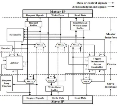
Fig 3.bus architecture supporting tagged transactions
Fig. 3 shows a bus system with single master and single slave. If masters (m slaves) are to be employed, copies of the components in the master (slave) interface should be employed, whereas only one copy of the components in center is needed. Tagged transactions are starts with a master issuing a request with an ID to a bus. In request phase, if Request Buffer in the bus is not full, the bus acknowledges that master and request is stored in a Request Buffer. Decoder will decodes the transaction address of the request, and Arbiter arbitrates whether any request can granted to access a target slave. If it is granted, then the Arbiter forwards the request to a slave by controlling the corresponding multiplexors, and index of target slave will recorded in one of the Recorders, in that way the transactions with same tag are recorded in the same Recorder. The number of Recorders is equal to the number of IDs which the corresponding master can assign. Also size of each Recorder will be equal to pipeline depth means that it is just enough for record all transactions they are not completed. Request Busy Checker checks whether any of the request is completed or not for assist the arbitration. For any write request, that corresponding write data will stored in Write Data Buffer, and Tagged Transaction Access Controller controls all the multiplexors which decide from any of the master the write data are to be provided.
After the slave accepts that request, it will acknowledges that particular bus, and then acknowledgment is forwarded to Request Buffer under the control of Arbiter. In case of the response phase, slave responds to the bus with read data for a read transaction or a completion status of the written data for a write transaction. If responses can be accepted, that will stored in the Read Data and Write Status Buffer, which will acknowledges the slave. Then tagged transaction access controller controls the multiplexors which decide from which slave the response is provided and from which read data and write status buffer the acknowledgment comes from. Finally, the response will sent to the master when the master is able to receive it.
V. BUS STATUS GRAPH
As shown in Fig. 4. the prime edge is fromvertex IDd to vertex Sj which indicates that the transaction corresponding to the edge is requesting to access Sj and which is the first accepted transaction among all currently accepted but it is not completed transactions with the tag IDd. The nonprime edge is from the vertex Si to the vertex IDd means that corresponding transaction is mainly targeting Si but that is not the first accepted transaction among all the accepted but not completed transactions tagged with IDd.
Fig 4. Prime edge and non prime edge in BSG indicating Si is waiting for Sj because of IDd.
In SOC system contains two slaves, then there are two vertices in a slave vertex set, namely S1 and S2. The IDs can be either zero or one, so there will be also two vertices in the ID vertex set, named as ID0 as well as ID1 (respectively, refers to ID value zero and one).
Fig 5. Example of BSG indicating system is in unsafe state, BSG indicating system is in safe state.
When master in Fig. 2 first generates requestsT1, that is a prime edge from ID0 to S1appears in the BSG as shown in Fig. 5(a). The master again requests T2 it will accesses S2 with ID1.A prime edge from ID1to S2 will appear after T2 it is accepted by S2 as in Fig. 5(b). Whenever master requests T3 which accesses S2 with ID0, there will be an uncompleted transaction (T1) tagged with ID0. Thus Fig. 5(c) shows the nonprime edge from S2 to ID0 appears after request T3 is accepted by S2. Similarly, Fig. 5(d) indicates that a nonprime edge fromS1 to ID1 will appear afterT4 is accepted by the slave S1. In Fig. 5(d), a cycleexists in the BSG, and the bus system is in an unsafe state will lead to a bus deadlock.
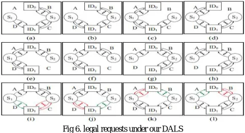
Fig 6. legal requests under our DALS
VI.HARDWARE IMPLEMENTATION
The hardware design of DALS attempts in order to stall the least number of transactions. In addition, with this we also target to complete decision of whether to stall a transaction in one clock cycle. We propose a hardware implementation which contains a number of waiting relation detectors and a number of unsafe state predictors which will altogether requires only one clock cycle for the stall decision.
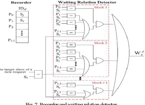
Fig. 7. Recorder and waiting relation detector.
1) Waiting Relation Detectors: here allocating a recorder for each ID in a bus system and index of a target slave of a tagged transaction is recorded in the corresponding recorder when the transaction is accepted by that slave. Responses from the different slaves with the same ID must be returned in the order that they are recorded in the recorder. Hardware implementation of the waiting relation detector detecting Wdij is shown in Fig. 7. left side shows a recorder in order to record the transactions with the tag IDd .
The P0 and P1are entries of IDd recorder in Fig. 8 shows that a request to Sj with IDd is accepted by Sj and then a request to Si with IDd is also accepted by Si. Now a new transaction is also tagged with IDd is again requested. The proposed waiting relation detector will detect waiting relations of already accepted requests as well as waiting relations if a new request is accepted as described below. As shown in Fig. 7, the waiting relation detector for Wdij contains:
l-1 blocks of circuits, where l is the size of the recorder
a comparator feeding the l-1 blocks
ORgate taking OR operation of the outputs of the l-1 blocks.
The comparator outside blocks determines whether a new request is targeting the Si or not. First comparator in block 1 determines whether the slave ID recorded in P0 is Sj or not, the remaining l-1 comparators determines that whether Si is stored in any location other than P0. This block will determines whether Si is waiting or will wait for Sj in P0 if a new request is accepted. Similarly, the circuits in block 2 will detect whether Si is waiting or will wait for Sj in P1 and so on. So all blocks together can detect whether the relation Wdij already exists or will exist if the new request is accepted.
Fig. 8. (a) Waiting table (b) Unsafe state predictor for the nontrivial cyclesb in the cycle group Wd1
12 &Wd223 &. . .&Wdkk1=1.
VII. ELASTIC BUFFER
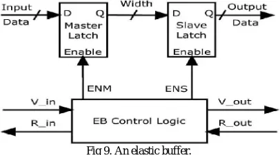
Request buffer, write data buffer and read and write status buffers are the major components in the bus design. There have been multiple proposals to eliminate these buffers in order to reduce area and power consumption. Elastic buffer (EB) flow control was recently proposed to eliminate router buffers while preserving buffering in the network. Pipeline flip-flop (FFs) become EBs with two storage locations through the addition of a small logic block which controls their master and slave latch enable inputs independently.
Fig 9. An elastic buffer.
The two inputs are still gated by the clock as in master-slave FFs. EBs can be implemented as custom cells to increase efficiency and guarantee that the two latches can never be enabled simultaneously. Having EBs in sequence enables channels to act as distributed FIFOs. Flits progress among EBs using a ready-valid handshake similar to the valid-stall handshake. Therefore, channels are used for buffering and router buffers are removed, eliminating the associated area and energy costs. EB networks trade off these savings for a wider data path that increases their throughput and makes them more energy and area efficient than VC networks. Fig. 9 shows an illustration of an EB.
VIII. ERROR DETECTION AND CORRECTION
Master and slave can communicate through bus either for read or write data. There may be chances for corrupting data during transmission from master to slave. In order to detect errors in data communication and processing, an additional bit is sometimes added to a particular binary code word to define its parity. A parity bit is an extra bit included to make the total number of 1’s in that resulting code word either even or odd. Parity may also be used with the binary numbers as well as with codes including ASCII.
The most common types of error-correcting codes are used in RAM are based on codes devised by R.W. Hamming.
Assume a 8-bit data word 11000100. We include 4 parity bits with this word and arranged the 12 bits as above. the parity bits can be found by,
The 8-bit data word is written into the memory together with the 4 parity bits as a 12-bit composite word. Substituting the 4 parity bits in their proper positions, we obtain the 12-bit composite word
C1, C2, C4, C8 are the check bits they are appending together and find C as C=C8 C4 C2 C1. If C=0, there is no error has occurred, If C!=0, the 4-bit binary number formed by the check bits gives the position of the erroneous bit if only a single bit is in error.
The error can then be corrected by complementing the corresponding bit. An error can occur in the data or in one of the parity bits.
IX.EXPERIMENTAL RESULTS
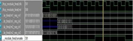
To compare the performance of the bus design with that of previous paper, we implement the on chip bus with elastic buffer techniques with the bus model shown in Fig. 3. So we can reduce the delay, power and area. The fig 10 is the simulation result of bus architecture with two master and single slave. Each master can use two id’s so in total four requests are generated.
fig 10. simulation result of bus architecture having two master and single slave under normal operation.
The simulation results of bus architecture supporting tagged transactions having two master and single slave under normal operation is shown above. The waveform from the Model Sim.clk is the clock signal, rst is the reset signal,req_in1, req_in2, req_in3, req_in4,are the 14 bit requests generated by master1 and master2 respectively. Unsafe is the signal that indicates whether the operation is safe or not.
The simulation results of bus architecture supporting tagged transactions having two master and single slave operations with dead lock are shown below. The waveform from the Model Sim. clk is the clock signal, rst is the reset signal,req_in1, req_in2, req_in3, req_in4,are the 14 bit requests generated by master1 and master2 respectively. Unsafe is the signal that indicates whether the operation is safe or not.
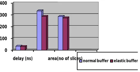
Table 1. comparison between bus architecture having normal and elastic buffer
Delay (ns)
Power (mW)
Area(no of slices)
bus architecture having normal buffer
33.591 333 286
bus architecture having elastic buffer
30.691 287 274
Comparison table shows that bus architecture having normal buffer requires more area overhead and delay than that of elastic buffer so by replacing normal request buffer, read and write status buffer, write data buffer can reduce the power requirement and cost as well.
fig 12. Comparison of normal and elastic buffer
X. CONCLUSION
Advanced communication protocols such as AXI can greatly improve the overall performance of a large VLSI system. However, the whole system may sink into a deadlock if designers do not carefully handle the advanced transactions. In this project, proposed a new graph model called the BSG to model the behaviour of a bus system that can describe the necessary and sufficient condition for an unsafe state to occur. Then the proposed technique is used to solve the deadlock problem. Elastic buffer in the proposed technique greatly outperforms with affordable area, delay and power .Encoding and decoding techniques avoid the occurrence of errors during write and read operation.
REFERENCES
1. Advanced Microcontroller Bus Architecture Specification. (1997)[Online]. Available: http://www.arm.com
2. Open Core Protocol Specification. (2006) [Online]. Available:http://www.ocpip.org/home
3. A. T. Tran and B. M. Bass, “RoShaQ: High-performance on-chip routerwith shared queues,” in Proc. IEEE 29th Int. Conf. Comput. Design, Oct. 2011, pp. 232–238.
4. J. Shao and B. T. Davis, “A burst scheduling access reordering mechanism,”in Proc. IEEE 13th Int. Symp. High Perform. Comput. Archit., Feb. 2007, pp. 285–294.
5. J. Pang, L. Yang, L. Shi, T. Zhang, D. Wang, and C. Hou, “A priorityexpression-based burst scheduling of memory reordering access,” inProc. Int. Conf. Embedded Comput. Syst., Archit., Model., Simul., Jul. 2008, pp. 203–209.
6. X. Xiao and J. J. Lee, “A true O(1) parallel deadlock detection algorithm for single-unit resource systems and its hardware implementation,” IEEE Trans. Parallel Distrib. Syst., vol. 21, no. 1, pp. 4–19, Jan. 2010.
7. A. Silberschatz, P. B. Galvin, and G. Gagen, Operating System Concepts, 7th ed. New York, USA: Wiley, 1993.
8. T. S. Cummins, “Method and apparatus for detecting a bus deadlock inan electronic system,” U.S. Patent 6 292 910, Sep. 18, 2001. 9. Technical Reference Manual of PrimeCell AXI Configurable Interconnect (PL300), ARM, Cambridge, U.K., 2010.
0 100 200 300 400
10. Chin-Yao Chang and Kuen-Jong Lee, “On Dead Lock Problem of on-chip bus supporting out-of order transactions”,IEEE Trans. on very large scale integr. (VLSI) Syst, vol. 22, no. 3, mar. 2014.
BIOGRAPHY