ABSTRACT
Prasad, Praveen. A Dynamically Reconfigurable Intrusion Detection
System. (Under the direction of Dr. Paul D Franzon)
A Dynamically Reconfigurable Intrusion Detection System
by
Praveen Prasad
A thesis submitted to the Graduate Faculty of
North Carolina State University
in partial fulfillment of the requirements for the Degree of
Master of Science
COMPUTER ENGINEERING
Raleigh
2003
Approved by
Dr. Paul D. Franzon, Chair of Advisory Committee
Biography
Acknowledgements
I would like to thank Dr.Paul Franzon for having given me the opportunity
to conduct this research. His guidance, tolerance and encouragement have
been invaluable to my success at graduate school. I would also like to thank
Dr.Eric Rotenberg and Dr.Rhett Davis for having served on my Advisory
Committee.
TABLE OF CONTENTS
LIST OF FIGURES vi
1. Introduction 1
2. Reconfigurable Computing 2
2.1 Spatial and Temporal Computation….……….3
2.2 Classification………5
2.3 Altera FLEX 10K FPGA………..6
2.4 FPGAs with Larger and Centralized Memory.……….8
2.5
Dynamically Programmable Gate Array (DPGA).…………..9
2.6
Run-Time Reconfiguration (RTR)………...9
2.7 PipeRench……… 10
2.8 Dynamically Programmable Cache (DPC)………..11
2.9 RRANN………12
2.10 Conclusion………12
3. Intrusion Detection 14
3.1 Classification………14
3.2 Anomaly detection………15
3.3 Misuse detection………...16
4. Dynamically Reconfigurable Intrusion Detection System 19
4.1 Motivations………...19
4.2 Structure of the DRIDS……….…..21
4.3 The Intrusion Detection Engine………..24
4.4 The Memory Controller………..25
4.5
The DRIDS Logical Element………..27
4.6 Multibit Output Look Up Table………..30
4.7 Conclusion.………..30
5. Implementation of the Snort Rule Set 31
5.1 The Snort detection engine………...31
5.2 Implementation of Snort Rule set on the DRIDS……… 33
5.3 Scoreboard Array………….………...…..37
5.4
Content Match Option……….. 38
5.5
Rule Header Processing………38
5.6
Content Match Option…….………..40
5.7
Dynamic Reconfiguration in DRIDS………44
5.8 Performance Analysis……….………...47
5.9 Conclusion……….………....48
6. Summary and Future Work 50
Bibliography 52
Appendix B: Verilog Code 57
List of Figures
Figure 2.1 Spatial and Temporal Pipelining………..3
Figure 2.2 Altera Logical Element………....7
Figure 2.3 Piperench Architecture………10
Figure 2.4 Dynamically Programmable Cache……….11
Figure 4.1 DRIDS Architecture……….22
Figure 4.2 DRIDS Logical Element………..26
Figure 4.3 SRAM Finite State Machine………....28
Figure 5.1 IDE Master FSM………..32
Figure 5.2 Snort Rule Chain Logical Structure……….34
Figure 5.3 Top Down Control in FSM Design………..36
Figure 5.4 Rule Format………..39
Figure 5.5 IDE FSM top-down distribution of control.……….41
Figure 5.6 Content Match FSM……….43
1. Introduction
An implementation of an Intrusion Detection System on a Dynamically
Reconfigurable Architecture is presented in this Thesis. The section on
Reconfigurable Computing contains a brief literature review on the topic in
areas relevant to this thesis. In the Intrusion Detection section, a background
on Intrusion Detection Systems is provided, elucidating its importance in a
networking environment. In Chapter 4 the architecture itself is presented
with a high level overview of the various Functional Units and their
interfaces. Chapter 5 discusses the implementation of a Network Based
Intrusion Detection System on the Dynamically Reconfigurable Architecture
along with a Performance Analysis. Suggestions for future improvements
and the challenges involved in implementing these are noted in the Future
Work section. The Appendix contain the Verilog code that models the
architecture and the implementation of Intrusion Detection on it.
2. Reconfigurable Computing
A Field Programmable Gate Array (FPGA) is an array of bit-processing
elements whose function and interconnection can be programmed after
fabrication. Most FPGAs use lookup tables (LUT) to serve as programmable
units. The lookup tables are wired together with a programmable
interconnect or switch fabric, which accounts for most of the area in each
FPGA cell. FPGAs were originally designed as user-programmable
alternatives to mask-configured gate arrays in which the bit-processing
elements implement the logic gates, and the programmable interconnect
replace the selective gate wiring.
LUT
The main advantage of reconfigurable computing derives from its unique
combination of broad applicability provided by the capability of
reconfiguration, and achievable performance, through the potential
exploitation of parallelism.
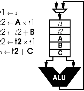
2.1 Spatial and Temporal Computation
Figure 2.1 from [1] depicts the difference between spatial and temporal
computing. In spatial computations, each operator exists at a different point
in space, allowing the computation to exploit parallelism, to achieve high
throughput and low computational latencies. In temporal implementations, a
small number of general compute resources are reused in time, allowing the
computation to be implemented compactly.
Computations are generally implemented in custom hardware or software.
Many systems are designed using a mixed approach, placing some subtasks
in custom hardware and some in software or more general purpose
processing engines. Hardware implementations offer high performance
because they do not involve the additional overhead for interpretation of
instructions or extra circuitry capable of solving a more general problem.
They are relatively faster due to the high parallelism and spatial execution.
Software implementations execute on a general-purpose processing engine
that interprets a designated data stream as instructions telling the engine
what operations to perform. As a result, software implementations are
flexible but relatively slow due to the temporal execution of instructions.
2.2 Classification
A reconfigurable device may be mainly characterized by the granularity of
the configurable units, the number of configuration levels (
contexts
), the
type of reconfiguration (
dynamic or static
), the computational model and the
memory organization.
A fine grain device provides the widest range of applicability at the expense
of efficiency. Coarse grain systems typically contain specially designed
units, which improves performance for specific areas.
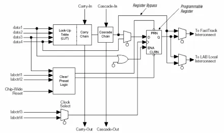
2.3 Altera FLEX 10K FPGA
Each FLEX 10K [6] device contains an embedded array to implement
memory and specialized logic functions, and a logic array to implement
general logic.
The embedded array consists of a series of Embedded Array Blocks (EAB).
When implementing memory functions, each EAB provides 2,048 bits,
which can be used to create RAM, ROM, dual-port RAM, or first-in first-out
(FIFO) functions.
When implementing logic, each EAB can contribute 100 to 600 gates
towards logic functions, such as multipliers, microcontrollers, state
machines, and DSP functions. EABs can be used independently, or
multiple EABs can be combined to implement larger functions.
machines—or combined across LABs to create larger logic blocks. Each
LAB represents about 96 usable gates of logic. Figure 2.2 depicts the
Logical Element used in the Altera FLEX 10k FPGA.
There are two types of routing, local and global. Local routing connects each
LE with its nearest neighbors and global routing can connect any two LEs on
the chip. Global routing comes with additional delay but is necessary to
implement large applications.
This dissertation stresses the use of coarse-grained reconfigurable arrays
with path widths greater than 1 bit because of the routing area overhead in
fine-grained architectures. A major benefit is the reduction in configuration
memory and configuration time as well as reduction in complexity of the
placement and routing.
2.4 FPGAs with Larger and Centralized Memory
There are two kinds of memory limitations on FPGAs: memory for
configurations and memory for data. The Dynamically Programmable Gate
Array (DPGA) offers a temporary storage for configuration and will be
discussed in the following section.
On-chip centralized memory is attractive for many FPGA architectures
because many applications implemented with FPGAs have large datasets
that cannot be stored in the FPGA. On-chip memory reduces memory access
latencies and the need for I/O resources.
2.5 Dynamically Programmable Gate Array (DPGA)
DeHon [7] defines utilization as the amount of logic used during the
execution of a subroutine. 100% utilization is highly desirable, however, in
most cases the FPGA fabric is utilized only a fraction of the time. With
DPGA, the main goal is to increase computational bandwidth while utilizing
100% of all logic. This is achieved by creating a storage area for
reconfigurations and having the FPGA fabric switch to different
configurations over time. A small DRAM is assigned to each LE that stores
different configurations. This is similar to partitioning the design over
several chips storing the partitions in memory and switching them over time.
2.6 Run-Time Reconfiguration(RTR)
2.7 PipeRench
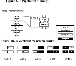
PipeRench [8] is a programmable data path that introduces a “virtual
hardware” abstraction by run-time reconfiguration of its programmable
hardware fabric. This addresses the problem of high cost of developing and
reusing hardware piplelines on reconfigurable devices. Applications
expressed in this hardware abstraction can run on a family of compatible
devices.
The top of figure 2.3 shows a 6-stage virtual hardware pipeline. The bottom
of this figure illustrates the first five cycles of reconfiguration of a four-stage
physical hardware pipeline executing the six stage virtual design.
Reconfiguration is performed by storing the configuration data of the entire
virtual hardware on-chip and moving this information from the on-chip
memory into the physical fabric every cycle.
2.8 Dynamically Programmable Cache (DPC)
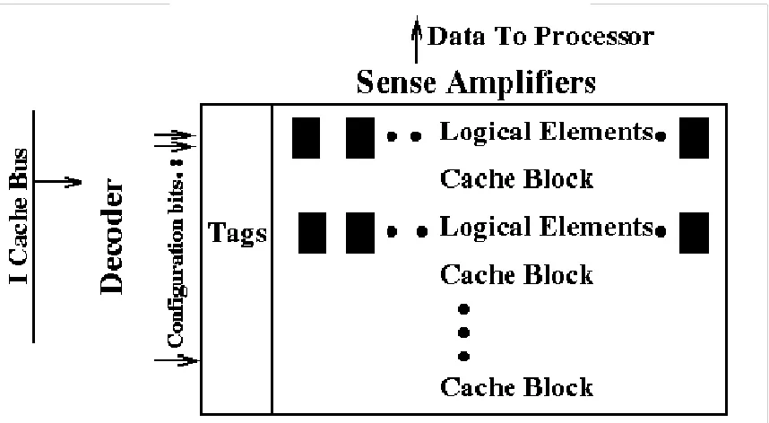
The DPC [9] is a run-time reconfigurable device that uses existing hardware
– cache memory – to store data and configuration information. This is
achieved by merging the data cache with the FPGA fabric on the same unit
as shown in figure 2.4.
This integration reduces communication bottlenecks with memory which
results in reduced reconfiguration latencies and decreased execution time.
The DPC, in concept, can act as a conventional data cache, a computational
device or a combination of the two. Figure illustrates how the logical
elements of the FPGA fabric are interspersed among the cache memory
blocks.
2.9 Run-Time Reconfiguration Artificial Neural Network
(RRANN)
The RRANN[18] uses run-time reconfiguration to increase the number of
hardware neurons an FPGA can implement. RRANN divides the
backpropagation algorithm into three, time-exclusive stages known as
feed-forward, backpropagation, and update. During execution, only one of the
three stages is configured on FPGAs. When that stage completes, the FPGAs
are reconfigured with the next stage. This process repeats itself until the
neural network converges on the training set.
2.10 Conclusion
3. Intrusion Detection Systems
Intrusion detection systems (IDSs) are software or hardware systems that
automate the process of monitoring the events occurring in a computer
system or network, analyzing them dynamically or statically for signs of
compromise to security. As network security breaches have increased in
number and severity in recent times, intrusion detection systems have
become a necessary addition to the security infrastructure of most
organizations.
Intrusions
can be defined as “attempts to compromise the confidentiality,
integrity, availability, or to bypass the security mechanisms of a computer or
network.” [11]
3.1 Classification
• Analysis - This part of intrusion detection systems actually organizes and
analyzes the events derived from the information sources, deciding when
those events indicate the occurrence of intrusions. The most common
analysis approaches are
misuse detection
and
anomaly detection
.
• Response – This is the set of actions that the system takes once an intrusion
is detected. These are typically grouped into active and passive measures,
with active measures involving automated intervention by the system, and
passive measures involving reporting IDS findings. There are two
approaches to analyzing events to detect attacks:
3.2 Anomaly detection
The main advantage of anomaly detection systems is that they can detect
previously unknown attacks. By defining what is normal, they can identify
any violation, whether it is part of the threat model or not.
3.3 Misuse detection
Misuse detection is a technique in which the analysis targets system activity,
looking for events or sets of events that match a predefined pattern of events
that describe a known attack. As the patterns corresponding to known
attacks are called
signatures
, misuse detection is sometimes called
signature-based detection. Misuse detection is the technique used by most commercial
systems and its most common form specifies each pattern of events
corresponding to an attack as a separate signature. The main advantage of
misuse detection systems is that they focus analysis on the audit data and
typically produce few false positives.
3.4 Network-Based IDSs
sensors are limited to running the IDS, they can be easily secured against
attacks. The majority of commercial intrusion detection systems are network
based.
3.4.1 Advantages of Network-Based IDSs:
•
A few well-placed network-based IDSs can monitor large networks.
•
The deployment of network-based IDSs has little impact upon
existing networks. Network-based IDSs are usually passive,
non-intrusive devices that listen on a network wire without interfering with
the normal operation of a network.
•
Network-based IDSs can be made very secure against attacks
themselves.
3.4.2 Disadvantages of Network-Based IDSs:
•
Many of the advantages of network-based IDSs don’t apply to more
modern switch-based networks. Most switches do not provide
universal monitoring ports and this limits the monitoring range of a
network-based IDS sensor to a single host.
•
Network-based IDSs cannot analyze encrypted information.
4. Dynamically Reconfigurable Intrusion Detection
System (DRIDS)
Reconfigurable devices (FPGAs) are flexible; have broad applicability and
provide high computational density and higher performance, through the
potential exploitation of parallelism. However, typical applications that use
FPGAs do not exploit their full computational density because of the limited
FPGA memory, inefficient FPGA utilization, processor to FPGA
communication bottlenecks and high reconfiguration latencies.
This thesis presents a reconfigurable architecture for a Network Based
Intrusion Detection System that provides a solution to these problems and
leverages the improvements to address the challenges in this application.
4.1 Motivations
quickly also forces some IDSs to compromise on detection
effectiveness.
•
Network-based IDSs have problems dealing with attacks that involve
fragmenting packets.
•
There are constant modifications being made to the algorithms that are
involved in network-based Intrusion Detection and also new additions
made to Rule-set that is used to identify attacks.
The implementation of such an application on Reconfigurable hardware will
result in a high performance gain on a non-intrusive and flexible system.
There are three primary ways to implement security functions in networking
hardware equipment as discussed in [13].
The method that is commonly used today id to use a co-processor with a
network processor or general-purpose processor. With higher data rates, this
method becomes less practical because the packet must traverse shared
resources such as data buses or memory four times.
processor must perform many of the same functions that the network
processor must do such as packet reassembly; thus work must be repeated
and silicon area must be duplicated.
The third method is to add the security functionality into the same silicon as
the network processor, thus adding security functionality into the network
processor and minimizing new silicon area. Such an approach solves the
problem of having the security processor to do many of the functions that the
network processor is targeted for. Some of these tasks include reassembly of
packets, protocol processing and exception handling. The DRIDS unit fits
into such an ASIC or programmable Network Processor environment.
4.2 Structure of the DRIDS
CTLR_RDY DO DO DO DO DO DO DO DO DO DO DO DO DO DO D DO RA RA RA RA RA RA RA RA RA RA RA RA RA RA RA RA SBD_DATA SBD_DATA SBD_DATA SBD DATA SramState SramState SramState SramState WrEn WrE WrEn WrEn PKT_DATA PKT_DATA PKT_DATA PKT_DATA PKT_RDY WrAddr RdWrAddr RdWrAddr IDE_RDY IDE_RDY IDE_RDY IDE_RDY
CONTROLLER0
IDE0
SRAM0
IDE3
IDE2
IDE1
SRAM3
SRAM2
SRAM1
CONTROLLER1
CONTROLLER2
CONTROLLER3
SCOREBOARD
The Intrusion Detection Engine is responsible for the actual implementation
of the signature based attack detection algorithm. It is controlled by a Finite
State Machine (FSM) with an array of 16 Reconfigurable Logical Elements
(LE Array) on the data-path. All computations are handled by the LE Array
and the FSM generates the configuration bits for the LE Array according to
the requirement of the current cycle.
Each IDE has a 2KB synchronous SRAM associated to it. The IDEs have
Read access to the SRAM through 4 32 bit ports. The SRAM has a width of
256 bits and a depth of 64 and allows 32 bit accesses through sub-field
extractions.
The Memory Controllers are responsible for the transfer of packet data from
one stage of the pipeline to the next. They are capable of detecting idle IDEs
and transferring packet data to them using 256 bit wide burst writes to the
SRAM. Each MC maintains a Finite State Machine of its corresponding
SRAM.
maintains a record of the result for each rule for all outstanding packets in
the DRIDS. This facilitates an external application (Hardware or Software)
to detect the content of a packet and decide if the packet is to be dropped,
ignored or flagged as suspicious.
4.3 The Intrusion Detection Engine
be discussed in greater detail in the chapter on the implementation of
rule-based Intrusion Detection on the DRIDS.
4.4 The Memory Controller
The SRAM memory controller for each stage of the DRIDS pipeline polices
the integrity of the data in the SRAM and generates controls to the
corresponding IDE to indicate the arrival of fresh packet data.
The first and last stages of the Memory Controllers are unique in the
following ways. MC0 handshakes with the external input (PKT_RDY) by
generating the CTLR_RDY signal to indicate that it is ready to accept new
packet data. MC3 does not require a mechanism to keep track of idleness in
following stages. In all other respects, the four Memory controllers are
similar.
There are four possible SRAM states; Invalid, Exclusive, Stalled and Valid.
The Invalid state is the one the SRAM adopts upon Reset. The Memory
Controller may write to this SRAM only if it is in the ‘Invalid’ state. A write
to the SRAM sends it to the ‘Exclusive’ state, which indicates that the
packet data in this SRAM is exclusive to it and not to be overwritten. Upon a
Read to this SRAM (which is equivalent to write to the SRAM in the
following stage) the state changes to ‘Valid’. This indicates that the contents
Reset/Initial State
Valid
Stalled
Exclusive Invalid
WrEn[n+1]
IDE_RDY[n] IDE_RDY[n] WrEn[n]
S0 S3
S0
S1
WrEn[n+1]
S2
of the SRAM have been read by the following stage but the corresponding
IDE has not completed the rule-checking. Similarly, if the IDE indicates the
completion of the rule-checking, the SRAM state changes to ‘Stalled’,
indicating that the following pipe stage has not read the information and the
Memory Controller waits on the following stage to complete and initiate a
‘Read’ before it can begin fetching packet data from the preceding stage or
from the external input. In order to avoid large delays in the ‘Stalled’ stage,
the Memory Controller begins fetching packet data soon after the first
‘Read’ cycle to it’s corresponding SRAM. Since the packet data transfer
occurs in bursts and because stage n+1 is always one cycle ahead of stage n,
there is no danger of data getting corrupted.
4.5 The DRIDS Logical Element
The Logical Elements used in this design are based on the Altera FLEX 10K
LEs discussed previously. However, there are certain unique features about
the LE in the DRIDS.
Data1
Figure 4.4 shows a single LE. The input for the LE are Data and
Configurations. The data signals are DATA0, DATA1, DATA2, DATA3
and CARRY_IN. The configuration signals are Sram_Op,
CascadeMux_select, RegBypass_enable, Reg2Datain_enable, Carry_enable
and Reg_enable. These configuration bits are generated by the FSM in the
Intrusion Detection Engine.
Reg_out[1]
Reg_out[0]
Compute_out
Data3 Data2
Reg_enable
Cascade_out[1: LE_out[1:0] Carry_out
Sram_Op
CascadeMux_select
RegBypass_enable
Regout2Datain_Enable Reset
Clock Data0 Carry_enable
Carry_in
SRAM0 SRAM1
The SRAM blocks of the LE hold the output of the functional unit for all
possible data combinations. For example, if the LE is to perform an ADD,
the output of the SRAM will be the addition of the two operands for all
possible input combinations.
The LE contains two memory units (flip-flops) that can store the results of
one previous cycle. This is particularly useful for this application where
address computations of the previous cycle are required for the memory
access of the current cycle. This will be explained in further detail in the
following chapter.
The functions of each configuration signal are as follows:
The
‘Sram_Op’
signal selects the function (arithmetic or logical) of the LE.
‘CascadeMux_select’
multiplexes Carry_out and Compute_out to
Cascade_out.
‘RegBypass_enable’
determines if LE_OUT needs to be the
output of the memory units (Data from a previous cycle) or Compute_out
(Output of SRAM).
‘Reg2Datain_enable’
determines if the input data to the
SRAM needs to be the output of the memory units.
‘Carry_enable’
signals
that there is an input carry when the LE operates in a cascaded mode and
4.6 Multibit Output Look Up Table
1-bit output granularity of each Look Up Table (LUT) in the LE results in a
large interconnect area and large delay due to a number of switches for the
programmability. [20] In order to avoid these and to provide greater data
width per LE Array, this thesis proposes to use an LE with multibit output
LUTs. Since multibit output LUT has the same inputs for all output bits, it is
less flexible in implementing functions. [10] However, it is not a major
bottleneck in this application as the reconfiguration is local and the
configurations supplied to LEs in a particular area are identical per cycle.
4.7 Conclusions
5. Intrusion Detection using the Snort Rule Set
Snort[15] is a cross-platform, network intrusion detection tool that can be
deployed to monitor TCP/IP networks and detect a wide variety of
suspicious network traffic as well as outright attacks. The program is free
software; access rights to it falls under the terms of the GNU General Public
License.
5.1 The Snort detection engine
Snort version 1.2.1 has the following option fields available:
1.
content: Searches the packet payload for the a specified pattern.
2.
flags: Tests the TCP flags for specified settings.
3.
ttl: Checks the IP header's time-to-live (TTL) field.
Chain Option
Content TCP Flags ICMP Codes/types
Payload Size
Etc.
Chain Header
Source IP Address Destination IP Address
Source Port Destination Port
Chain Header
Source IP Address Destination IP Address
Source Port Destination Port
Chain Header
Source IP Destination IP Source Port Destination Port
Chain Option
Content TCP Flags ICMP Codes/types
Payload Size
Etc.
Chain Option
Content TCP Flags ICMP Codes/types
Payload Size
Etc.
4.
itype: Match on the ICMP type field.
5.
icode: Match on the ICMP code field.
6.
minfrag: Set the threshold value for IP fragment size.
7.
id: Test the IP header for the specified value.
8.
ack: Look for a specific TCP header acknowledgement number.
9.
seq: Log for a specific TCP header sequence number.
10.
logto: Log packets matching the rule to the specified filename.
11.
dsize: Match on the size of the packet payload.
12.
offset: Modifier for the content option, sets the offset into the packet
payload to begin the content search.
13.
depth: Modifier for the content option, sets the number of bytes from
the start position to search through.
14.
msg: Sets the message to be sent when a packet generates an event.
5.2 Implementation of Snort Rule set on the DRIDS
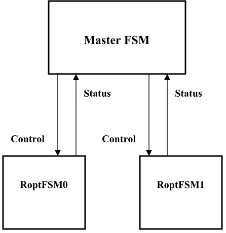
that occurs. When the RoptFSM completes checking its rule option, it
returns control to the Master FSM which then proceeds to check the next
rule option.
SramState=Exclusive
OptFSM_Fail OptFSM_Pass Option#=RuleDelimiter
Option#=RuleDelimiter
Option#=ValidRule& !ContentMatch Option#=Final
S0 IDE_RDY=1 SCBD EN=0
Reset/Initial State
S4 IDE_RDY=0 SCBD EN=0
S3 IDE_RDY=0 SCBD EN=1 S1
IDE_RDY=0 SCBD EN=1
S2 IDE_RDY=0 SCBD EN=0
As shown in Figure 5.2 , the Master FSM has 5 possible states. Upon Reset
the FSM enters into state S0. In this state it maintains the IDE_RDY signal
at ‘1’ saying that the IDE is not currently processing a packet. It also
initializes the Read Pointer to the location of the first Rule in the SRAM. In
this state, the FSM is sampling the SramState signal from the controller for
this pipe stage, and remains in this stage as long as the SramState is
“Invalid”.
The FSM transitions to state S1 when SramState changes to “Exclusive”.
This state checks against the rule option read in from the SRAM and passes
control to the RoptFSM that handles it. This state also deduces the number
of bytes by which to increment the Read Pointer from the current option
being handled by the RoptFSM. But this value cannot be deduced upon a
content match option and this triggers a transition to state S2. For all other
options, the FSM transitions to state S3.
After incrementing the Read Pointer to point to the next valid rule in SRAM,
the FSM transitions to State S3.
S3 is a stalled state where the FSM waits for return of control from the
RoptFSM. The RoptFSM could return with either a “Pass” or a “Fail”
message. If a Rule option fails, the Master FSM updates the Scoreboard
saying that the particular rule has failed and moves on to the next Rule in the
SRAM. However, in order to find the next rule in the SRAM, the FSM
needs to find the rule delimiter for the current rule and hence enters sate S4
where it increments the ReadPointer until the rule delimiter is found at
which point it return to state S1.
Status Status
Control Control
Master FSM
RoptFSM0 RoptFSM1
On a passing rule option in state S3, i.e. the RoptFSM returns control with a
“PASS” signal, the Master FSM transitions to state S1 where it proceeds to
read the next rule option from the SRAM. Upon finding a rule delimiter,
state S1 updates the Scoreboard. Figure 5.3 from [21] illustrates the design
approach adopted for the DRIDS IDE.
5.3 Scoreboard Array
The Scoreboard contains logic to determine the serial number of the rule
whose status is currently being updated by an IDE. Each incoming packet is
assigned a Tag value by the SRAM controller of Stage 1 using the Least
Recently Used (LRU) algorithm. This value is communicated to the IDE that
is processing that packet and the invalid bit is set in the Scoreboard against
the tag of the packet currently being processed. This indicates to the external
application that is reading the scoreboard that the corresponding packet is
currently being processed. The IDEs use the tag of the packet to index into
the Scoreboard. The IDE at the final pipe stage resets the invalid bit on the
5.4 Rule Format
The rules are stored in a dedicated section of the SRAM in the format
illustrated in Figure 5.3. The Rule Header contains the protocol field as well
as information regarding the Source and Destination IP Addresses and Ports
in the encapsulated Rule. This is followed by the actual Addresses and Ports,
if any, as indicated by the header. The Header encapsulates the Rule
Options. Each option begins with an Option Delimiter that tells the Master
FSM the nature of the option that follows. At the end of every rule there is a
Rule Delimiter that indicates to the Master FSM that the current rule is
complete. Such a consistent format of encoding the rules in the SRAM
allows the DRIDS to implement an optimum number of rules with limited
memory.
5.5 Rule Header Processing
be applied to the rule's address and any incoming packets that are tested
against the rule. A CIDR block mask of /24 indicates a Class C network, /16
a Class B network, and /32 indicates a specific machine address.
1:0 1:0 3:0 31:0 15:0 31:0 15:0 3:0 X:0 3:0
Rule Header
Rule Options
Protocol
Source/Dest Port Enable
Source/DestAddress
Source Address (if any)
Source Port (if En)
Rule Option Option Delimiter Dest Port (if En) Dest Address (if any)
Rule Delimiter
5.5 Rule Header Processing
The DRIDS Rule Header determines the type of packet, its source and
destination. The first field in a rule is the protocol. There are four Protocols
that the DRIDS currently analyzes for suspicious behavior - tcp, udp, icmp,
and ip. The next portion of the rule header deals with the IP address and port
information for a given rule. A straight numeric IP address and a CIDR
block form the addresses. The CIDR block indicates the netmask that should
be applied to the rule's address and any incoming packets that are tested
against the rule. A CIDR block mask of /24 indicates a Class C network, /16
a Class B network, and /32 indicates a specific machine address.
The DRIDS implements the rule header using a Finite State Machine called
the Header FSM, Figure 5.4, which is the first Ropt FSM that is invoked by
the Master Controller.
5.6 Content Match Option
Load Dest. Port
Compare Address Registers
Load Dest. IP
Load Dest. Network
CIDR Masking Dest. Addr Check Compare Address
Registers
CIDR Masking
Load Source Port
Load Source Network Load Source IP
S0
S1
S2
S3
S4
S5
S6
S7
S8
S11
S10
S9
S13
S12
Reset/Initial State Protocol Check Source Addr Check
If a content check is required, Snort uses a Boyer-Moore pattern matching
algorithm to check the content string held in the Rule Option against the
entire packet payload. If no match exists, Snort will proceed to the next Rule
Option in the list.
Boyer-Moore is a rather famous pattern-matching algorithm that is quite fast
in practice. It uses heuristics to reduce the number of comparisons needed to
determine if a given text string matches a particular pattern, i.e. it uses
knowledge of the keyword to search for to skip over unnecessary
comparisons against the text being searched. The algorithm typically aligns
the text and the keyword to search for so that the keyword can be checked
from left to right along the text string beginning with the last character of the
keyword and ending with the first.
The first heuristic it uses is commonly referred to as a
bad character
occurrence of a substring that matches what has already been successfully
matched. Figure 5.5 depicts the implementation of an Exact Pattern Match
using the Boyer-Moore Algorithm.
In the case of the DRIDS, since the pattern matching is in binary, the
bad
character
heuristic will not be very helpful because there are only two
possibilities for characters that cause the mismatch and they are both likely
to be in the pattern. However, the bits can be arranged together to make
Mismatch
Content Match Complete Reset/Initial
Figure 5.6 : Content Match FSM (RoptFSM1)
S0
S2
S3
S1
Configure LE as Comparator and Flop Match Length
Read Pattern Size and Compute Max Match Length in Skip Table
“characters” and the
repeated substring
heuristic may be exploited to an
advantage.
5.7 Dynamic Reconfiguration in DRIDS
The Content Matching option is the most computationally intensive
procedure in Snort’s Signature based Intrusion Detection scheme. Despite
the significant speedup achieved by the optimized algorithm, Snort spends
significant time in exact pattern matching, using up precious processor
cycles.
The transition from state S2 to S3 triggers a context switch in the Logical
Elements from a 16 bit adder to a 16 bit comparator. The adder is used in the
computation of new indices into memory and the comparator is used for the
Exact Pattern Matching. The FSM loads each configuration to the FPGA as
necessary at run-time. In this manner the application is divided into a series
of sequentially executed stages with each stage implemented as a separate
context for the IDE. RTR can increase the functional density and
Single Cycle Context Switch State Change
Match Size DI
Configurations
New Txt Ptr Txt Ptr
Configurations
LE_Array 16 bit Adder
LE_Array 16 bit Comparator
S2 S3
Figure 5.6 Dynamic Reconfiguration in the DRIDS
performance of an application when compared to single context FPGAs by
taking advantage of the idle circuitry of each stage.
The potential drawback of RTR is the latency associated with
reconfiguration and the challenges posed by the transmission of intermediate
results from one configuration to the next. In the DRIDS architecture,
reconfiguration latencies are significantly reduced because of the
configuration bits being generated from the FSM logic and not loaded from
an external memory. The single cycle reconfiguration latency aids in the
transmission of intermediate results between configurations, as the results
from the previous cycle are available to the LE Data inputs in the following
configuration cycle.
5.8 Performance Analysis
The DRIDS Master FSM and Content Match FSM were designed, validated
and synthesized. Being the most computationally intensive procedure in the
Intrusion Detection System, the Content Match FSM was identified as the
bottleneck in the performance of the DRIDS system.
In simulation, the Content match FSM took an average of 148 cycles to
match a 64 bit pattern; (Snort Content Match patterns range from 4 bits to
130 bits) with a 37% improvement from using the Boyer Moore Algorithm
instead of using a brute-force approach.
Running on a 20 ns clock, with a parallel implementation of optional FSMs,
the entire DRIDS system will run at 50 MHz. With sufficient capacity to
hold 50 rules per SRAM, each pipe stage will have an execution time as
follows:
Execution Time = Rule Count * Cycle Time * Cycles per Rule
= 50 * 20ns * 148
Speedup due to pipelining = # of pipe stages = 4
Hence the processing time for a single packet in the DRIDS is 37
µ
S. This
equates to a throughput of 0.32 Gbps as the DRIDS processes IP packets of
1500 octets. (MTU of Ethernet)
This is a significant speedup over the current software implementations that
run at 25 Mbps as per the experimental results by Cho et al. in [21]. This
approach also retains the programmability and flexibility of the system by
storing the rules in embedded SRAM and using them as instructions to the
DRIDS. Moreover, there are significant area improvements over previous
hardware implementations of this system [21] where the rules are embedded
in the hardware, leading to a decrease in the number of rules that may be
implemented. Using the DRIDS approach and an effective Rule Optimizer,
all Snort rules currently in use may be implemented in the system.
5.9 Conclusions
6. Summary and Future Work
6.1 Summary
R
econfigurable Devices are used extensively by designers due to their ability
to provide Rapid Prototyping and Unlimited Reconfiguration. However,
because of the similarity with conventional design approaches, almost all
reconfigurable logic applications are compile-time configured. The lack of
sufficient design tools and a well-defined methodology prevents the
wide-spread use of techniques such as Run-Time Reconfiguration. There are few
entire applications [19] that have been implemented with run-time
reconfiguration. The area is one that could be further leveraged with some
extensive exploration.
6.2 Future Work on the DRIDS
Snort Rule Optimizer
Multi-Pattern Search
A Multi-Pattern Search algorithm could be adopted in the Rule Checking
phase to attain maximum speedup and avoid redundant comparisons. This
would tremendously increase the parallelism in the application and could be
treated as an area that could leverage the spatial computations of
Reconfigurable Devices.
Anomaly Detection
BIBLIOGRAPHY
[1] Andre DeHon and John Wawrzynek “Reconfigurable Computing : What,
Why, and Implications for Design Automation.”
Proceedings of the 1999
Design Automation Conference,
pages 610--615, June 1999
[2] P. Lysaght, “Aspects of Dynamically Reconfigurable Logic”,
in IEE
Colloquium on Reconfigurable Systems,
Glasgow, Scotland, pp 1-5, Mar
1999
[3] Reiner Hartenstein, “Coarse-Grained Reconfigurable Architectures”,
ASP-DAC 2001
[4] Andre DeHon “The Density Advantage of Configurable Computing”
IEEE Computer
, 33(4):41--49, April 2000
[6] “ALTERA FLEX 10K Embedded Programmable Logic Device Family
Datasheet”
www.altera.com
[7] A. DeHon, “Dynamically programmable gate array: A step towards
increased computational density”
FPGA’ 96 – Fourth Canadian Workshop
on Filed Programmable Devices,
vol. 1, pp. 13-14, 1996
[8] Herman Schmit, David Whelihan, Andrew Tsai, Matthew Moe,
Benjamin Levine, R. Reed Taylor “PipeRench: A Virtualized Programmable
Datapath in 0.18 Micron Technology”
2002 IEEE Custom Integrated
Circuits Conference (CICC)
.
[9] Mouna Nakkar, “Evaluation of Dynamically Programmable Cache
Machine with Low Power Field Programmable Gate Arrays (FPGAs) and
3-Dimensional Multi-Chip-Module Package”
1999 PhD. Dissertation, Dept. of
ECE, NCSU
on Very Large Scale Integration (VLSI) Systems,
Volume: 9 Issue: 4
Page(s): 509 –523
[11] Rebecca Bace; Peter Mell, “NIST Special Publication on Intrusion
Detection Systems”
[12] Richard A. Kemmerer and Giovanni Vigna, “Intrusion Detection: A
Brief History and Overview”
[13] Feghali, W., Burres, B., Wolrich, G., Carrigan, D., “Security: Adding
Protection to the Network via the Network Processor.”
Intel Technology
Journal
. http://developer.intel.com/technology/itj/2002/volume06issue03/
(August 2002).
[14] Robert Sedgewick,
Algorithms
. Addison-Wesley Publishing Company,
1988.
[16] C. Jason Coit, Stuart Staniford, Joseph McAlerney, “Towards Faster
String Matching for Intrusion Detection or Exceeding the Speed of Snort”
www.silicondefense.com
[17] Boyer R.S
,
Moore J.S., “A fast string searching algorithm”
Communications of the ACM, 1977
.
20:762-772.
[18] Brad L.Hutchings, Michael J.Wirthlin, “Implementation Approaches for
Reconfigurable Logic Applications”
[19] James G.Eldridge, Brad L.Hutchings “Run-Time Reconfiguration: A
Method for Enhancing the Functional Density of SRAM-based FPGAs”
[20] A. DeHon, “Balancing interconnect and computation in a
reconfigurable computing array (or, why you don’t really want 100% LUT
utilization),” in
Proc. FPGA’99
, Feb. 1999.
International Converence on Field-Programmable Logic and Applications,
Appendix : Verilog Code
/********************************************************************** * Block Name : IDE
* Author : Praveen Prasad
* Affiliation : North Carolina State University * Project : DRIDS - MS Thesis, May 2003 * Date : 04/16/2003
* Description : This module implements a single Intrusion Detection * Engine with Dynamically Reconfigurable Logical Elements on the Data
* Path.
**********************************************************************/ `include "logical_element.v"
module IDE(Reset, Clock, SramState, DI0, DI1, DI2, DI3, RA0, RA1, RA2, RA3);
input Reset, Clock; input [2:0] SramState; input [7:0] DI0, DI1; input [15:0] DI2, DI3;
output [10:0] RA0, RA1; output [11:0] RA2, RA3;
reg [10:0] RA0, RA1; reg [11:0] RA2, RA3;
reg [13:0] FSM_RDY, FSM_STAT; reg ROPT_RDY, ROPT_STAT;
/* Master FSM */
reg [10:0] ReadPtr, RulePtr, PktPtr; reg FsmTrackRegEn;
reg [3:0] FsmTrackReg; reg IDE_RDY;
reg ScbdEn; reg ScbdStat; reg [3:0] FsmStart; reg RulePtrAEn; reg [10:0] ReadPtrInc;
reg PatternSizeRegEn; reg [3:0] CurrentRule;
/* Rule Header FSM */ reg [31:0] HomeAddressReg; reg [31:0] HomeNetworkReg; reg [1:0] HomeCidrReg;
reg RuleAddrSel, AddrLoadCtrEn; reg [1:0] PktAddrSel;
reg [1:0] AddrLoadCtr;
reg [11:0] PatternPtr; reg [11:0] SkipPtr; reg RulePtr1En; reg PatternPtrDecEn; reg ContentPtrIncEn; reg ContentPtrReset; reg PatternPtrReset; reg [2:0] MatchSize;
reg [1:0] PatternOffset; reg EndOfPattern; wire EndOfPacket;
/* Configuration signals for LE Array */ reg Regout2Datain_enable;
reg RegBypass_enable; reg Reg_enable;
reg CascadeMux_select; reg Carry_enable; reg [2:0] Sram_Op;
reg Carry_in;
/* LE Array Data */ reg [15:0] Data1; reg [15:0] Data2;
/* LE Array Output */ wire [15:0] Result; wire [7:0] Carry_out; wire [15:0] Cascade_out;
/* State definitions for the finite-state machine */ parameter [2:0] /* synopsys enum states */
S0 = 3'd0, S1 = 3'd1, S2 = 3'd2, S3 = 3'd3, S4 = 3'd4, S5 = 3'd5;
reg [2:0] CurrentState, CurrentState1, NextState, NextState1;
parameter PASS = 1'b0; parameter FAIL = 1'b1; parameter FALSE = 1'b0; parameter TRUE = 1'b1;
parameter [3:0] PROTOCOL = 4'b1010; parameter [3:0] SRCIP = 4'b1101; parameter [4:0] DESTIP = 5'b10001; parameter [4:0] SRCPORT = 5'b10101;
parameter [4:0] DESTPORT = 5'b10111; parameter [11:0] CONTENT = 12'b000000101000;
/*--- * This block defines the interface between SRAM and IDE
always@(ReadPtr) RA1 = ReadPtr;
always@(DI1)
CurrentRule = DI1[7:4];
always@(ContentPtr) RA2 = ContentPtr;
always@(PatternSizeRegEn or ReadPtr or PatternPtr or CurrentState1 or SkipPtr)
begin
if(PatternSizeRegEn)
RA3 = (ReadPtr << 1) + 1'b1; else if(CurrentState1 == S3)
RA3 = SkipPtr; else
RA3 = PatternPtr; end
/*--- * Combinatorial Logic that selects the driver of Data 1 and Data 2 to * the Logic Elements.
*---*/ always@(CurrentState1 or DI1 or DI2 or DI3 or ContentPtr)
begin
case(CurrentState1) S0:
begin
Data1 = DI2;
Data2 = DI3;
end S1: begin
Data1 = DI2;
Data2 = DI3;
end
S2:/* No match on compare. Increment Content Ptr by 1 and reset Pattern Ptr*/
begin
Data1 = ContentPtr;
Data2 = 16'd1;
end
S3:/* 4, 8 or 12 bit match. Increment Content Ptr by Skip Table Entry and Reset Pattern Ptr*/
begin
Data1 = ContentPtr; Data2 = DI3[15:8]; end
S4: begin
Data1 = ContentPtr;
Data2 = 16'b0000000000000100; end
Data1 = DI2;
Data2 = DI3;
end default: begin
Data1 = DI2;
Data2 = DI3;
end
endcase end
/*--- * Master FSM
*---*/ always@(CurrentState or SramState or CurrentRule or ReadPtr or ROPT_RDY or ROPT_STAT or PatternSizeReg)
begin
case(CurrentState) /* synopsys parallel_case full_case */
S0: /* Initial State */ begin
IDE_RDY = TRUE; ScbdEn = FALSE; ScbdStat = TRUE; FsmStart = 4'b0000; FsmTrackRegEn = 1'b0; RulePtrAEn = FALSE; ReadPtrInc = 10'd0;
PatternSizeRegEn = FALSE; if(SramState == S1)
NextState = S1; else
NextState = S0; end
S1: /* Read Sram */ begin
IDE_RDY = FALSE; ScbdEn = FALSE; ScbdStat = TRUE; RulePtrAEn = TRUE;
ReadPtrInc = 11'b00000000000; FsmTrackRegEn = 1'b1;
case(CurrentRule)
4'b0000: /* Final Rule in SRAM */ begin
FsmStart = 4'b0000;
PatternSizeRegEn = FALSE;
NextState = S0;
end
4'b0001: /* Rule Delimiter */ begin
FsmStart = 4'b0000;
PatternSizeRegEn = FALSE;
NextState = S1;
begin
FsmStart = 4'b0010;
PatternSizeRegEn = TRUE;
NextState = S2;
end
4'b0011: /* ttl */
begin
FsmStart = 4'b0011;
PatternSizeRegEn = FALSE;
NextState = S3;
end
4'b0100: /* tos */
begin
FsmStart = 4'b0100;
PatternSizeRegEn = FALSE;
NextState = S3;
end
4'b0101: /* id */
begin
FsmStart = 4'b0101;
PatternSizeRegEn = FALSE;
NextState = S3;
end
4'b0110: /* ipoption*/ begin
FsmStart = 4'b0110;
PatternSizeRegEn = FALSE;
NextState = S3;
end
4'b0111: /* fragbits */ begin
FsmStart = 4'b0111;
PatternSizeRegEn = FALSE;
NextState = S3;
end
4'b1000: /* dsize */ begin
FsmStart = 4'b1000;
PatternSizeRegEn = FALSE;
NextState = S3;
end
4'b1001: /* flags */ begin
FsmStart = 4'b1001;
PatternSizeRegEn = FALSE;
NextState = S3;
end
4'b1010: /* seq */
begin
FsmStart = 4'b1010;
PatternSizeRegEn = FALSE;
NextState = S3;
end
4'b1011: /* ack */
begin
NextState = S3; end
4'b1100: /* itype */ begin
FsmStart = 4'b1100;
PatternSizeRegEn = FALSE;
NextState = S3;
end
4'b1101: /* icode */ begin
FsmStart = 4'b1101;
PatternSizeRegEn = FALSE;
NextState = S3;
end
4'b1110: /* icmp_id */ begin
FsmStart = 4'b1110;
PatternSizeRegEn = FALSE;
NextState = S3;
end
4'b1111: /* icmp_seq */ begin
FsmStart = 4'b1111;
PatternSizeRegEn = FALSE;
NextState = S3;
end endcase end
S2: /* Content Match Pointer Update */ begin
NextState = S3; IDE_RDY = FALSE; ScbdEn = FALSE; ScbdStat = TRUE; FsmTrackRegEn = 1'b0; RulePtrAEn = FALSE;
/* This is OK because the ROPT FSMs are no longer sampling this signal */
FsmStart = 4'b0000;
ReadPtrInc = PatternSizeReg; PatternSizeRegEn = FALSE;
end
/* S2 */
S3: /* Stall State that samples ROPT FSM o/p */ begin
IDE_RDY = FALSE; FsmStart = 4'b0000; ReadPtrInc = 10'd0; FsmTrackRegEn = 1'b0; RulePtrAEn = FALSE;
ScbdStat = TRUE; NextState = S0; end
else if(ROPT_RDY & !ROPT_STAT) begin
ScbdEn = TRUE; ScbdStat = FALSE; NextState = S0;
end else begin
ScbdEn = FALSE; ScbdStat = TRUE; NextState = S3;
end end
/* S3 */
default: begin
NextState = S0; IDE_RDY = FALSE; ScbdEn = FALSE; ScbdStat = TRUE; FsmStart = 4'b0000; RulePtrAEn = FALSE; ReadPtrInc = 10'd0; FsmTrackRegEn = 1'b0;
PatternSizeRegEn = FALSE;
end endcase
end /* always@ */
/*--- * Sequential Logic for assigning the Current State from Next State at * the positive edge of each clock cycle. Enables an asynchronous Reset * to cause FSM to reset to State 0.
*---*/ always@(posedge Clock or negedge Reset)
begin
if(!Reset)
#1 CurrentState = S0; else
#1 CurrentState = NextState; end /* always@ */
/*--- * This block also updates the Read pointer at every positive edge of clock.
* This is initialised to the 47th Row of memory, where the Rules begin *---*/ always@(posedge Clock or negedge Reset)
begin
if(!Reset)
#1 ReadPtr = 11'b10111000000; else
#1 ReadPtr = ReadPtr + ReadPtrInc; end /* always@ */
/*--- * Sequential Logic that keeps track of the currently active FSM
* Controlled by Master FSM
*---*/ always@(posedge Clock or negedge Reset)
begin
if(!Reset)
#1 FsmTrackReg = 4'b0000; else if (FsmTrackRegEn)
#1 FsmTrackReg = FsmStart; end
/*--- * Combinatorial Mux for Rule Header and Rule Option FSM Status Updates to
* Master FSM. Controlled by Master FSM updated by all Ropt FSM
*---*/ always@(FsmTrackReg or FSM_RDY or FSM_STAT)
begin
case(FsmTrackReg)
4'b0000: /* Final Rule in SRAM */ begin
ROPT_RDY = 1'b0;
ROPT_STAT = 1'b0; end
4'b0001: /* Rule Delimiter */ begin
ROPT_RDY = 1'b0; ROPT_STAT = 1'b0; end
4'b0010: /* Content Match */ begin
ROPT_RDY = FSM_RDY[0]; ROPT_STAT = FSM_STAT[0];
end
4'b0011: /* ttl */ begin
ROPT_RDY = FSM_RDY[1]; ROPT_STAT = FSM_STAT[1]; end
4'b0100: /* tos */ begin
ROPT_RDY = FSM_RDY[2]; ROPT_STAT = FSM_STAT[2]; end
4'b0101: /* id */ begin
ROPT_RDY = FSM_RDY[3]; ROPT_STAT = FSM_STAT[3]; end
ROPT_RDY = FSM_RDY[4]; ROPT_STAT = FSM_STAT[4]; end
4'b0111: /* fragbits */ begin
ROPT_RDY = FSM_RDY[5]; ROPT_STAT = FSM_STAT[5]; end
4'b1000: /* dsize */ begin
ROPT_RDY = FSM_RDY[6]; ROPT_STAT = FSM_STAT[6]; end
4'b1001: /* flags */ begin
ROPT_RDY = FSM_RDY[7]; ROPT_STAT = FSM_STAT[7]; end
4'b1010: /* seq */ begin
ROPT_RDY = FSM_RDY[8]; ROPT_STAT = FSM_STAT[8]; end
4'b1011: /* ack */ begin
ROPT_RDY = FSM_RDY[9]; ROPT_STAT = FSM_STAT[9]; end
4'b1100: /* itype */ begin
ROPT_RDY = FSM_RDY[10]; ROPT_STAT = FSM_STAT[10]; end
4'b1101: /* icode */ begin
ROPT_RDY = FSM_RDY[11]; ROPT_STAT = FSM_STAT[11]; end
4'b1110: /* icmp_id */ begin
ROPT_RDY = FSM_RDY[12]; ROPT_STAT = FSM_STAT[12]; end
4'b1111: /* icmp_seq */ begin
ROPT_RDY = FSM_RDY[13]; ROPT_STAT = FSM_STAT[13]; end
endcase end
/*--- * FSM1 - Content Match FSM : Uses the Boyer Moore Algorithm to perform an
* an Exact Pattern Match on the packet content.
always@(CurrentState1 or EndOfPacket or EndOfPattern or FsmStart or Result or MatchSize or PatternOffset)
begin
Regout2Datain_enable = FALSE; RegBypass_enable = TRUE;
Reg_enable = FALSE;
CascadeMux_select = FALSE; Carry_enable = TRUE; Carry_in = 1'b0;
case(CurrentState1) /* synopsys parallel_case full_case */ S0: /* Initial State */
begin
PatternPtrReset = TRUE; ContentPtrReset = TRUE; PatternPtrDecEn = FALSE; ContentPtrIncEn = FALSE; RulePtr1En = TRUE;
Sram_Op = 3'b111;
if(FsmStart == 4'b0010) begin
FSM_RDY[1] = TRUE;
FSM_STAT[1] = TRUE;
NextState1 = S5;
end else begin
FSM_RDY[1] = FALSE;
FSM_STAT[1] = TRUE;
NextState1 = S0;
end end
/* S0 */
S5: /* Stall State */ begin
PatternPtrReset = TRUE; ContentPtrReset = TRUE; PatternPtrDecEn = FALSE; ContentPtrIncEn = FALSE; RulePtr1En = TRUE;
Sram_Op = 3'b111;
FSM_RDY[1] = FALSE;
FSM_STAT[1] = TRUE;
NextState1 = S1;
end /* S0 */
S1: /* Read Content Size and Compute Max. Entry in Skip Table */
begin
RulePtr1En = FALSE;
ContentPtrReset = FALSE;
Sram_Op = 3'b111;
/* This is where you update the values of the Pattern Pointer and Content Pointer.
2'b00: begin
FSM_RDY[1] = FALSE;
FSM_STAT[1] = TRUE;
case(MatchSize) 3'b001: begin
PatternPtrReset = TRUE;
PatternPtrDecEn = FALSE;
ContentPtrIncEn = FALSE;
NextState1 = S3;
end 3'b010: begin
PatternPtrReset = TRUE;
PatternPtrDecEn = FALSE;
ContentPtrIncEn = FALSE;
NextState1 = S3;
end 3'b011: begin
PatternPtrReset = TRUE;
PatternPtrDecEn = FALSE;
ContentPtrIncEn = FALSE;
NextState1 = S3;
end 3'b100: begin
/* This is the only time we go to S4. It means we're on to a
pattern! Here the LE Array becomes a subtractor */
PatternPtrReset = FALSE;
PatternPtrDecEn = TRUE;
ContentPtrIncEn = FALSE;
NextState1 = S4;
end
default: begin
PatternPtrReset = TRUE;
PatternPtrDecEn = FALSE;
ContentPtrIncEn = FALSE;
NextState1 = S2;
end endcase end
3'b001: begin
PatternPtrReset = FALSE;
PatternPtrDecEn = FALSE;
ContentPtrIncEn = FALSE;
NextState1 = S0;
FSM_RDY[1] = TRUE;
FSM_STAT[1] = FALSE;
end 3'b010: begin
PatternPtrReset = FALSE;
PatternPtrDecEn = FALSE;
ContentPtrIncEn = FALSE;
NextState1 = S0;
FSM_RDY[1] = TRUE;
FSM_STAT[1] = FALSE;
end 3'b011: begin
PatternPtrReset = FALSE;
PatternPtrDecEn = FALSE;
ContentPtrIncEn = FALSE;
NextState1 = S0;
FSM_RDY[1] = TRUE;
FSM_STAT[1] = FALSE;
end 3'b100: begin
/* YOu're onto a pattern at the end of the packet, unlikely corner case. */
PatternPtrReset = FALSE;
PatternPtrDecEn = TRUE;
ContentPtrIncEn = FALSE;
NextState1 = S4;
FSM_RDY[1] = FALSE;
FSM_STAT[1] = TRUE;
end endcase end 2'b10: begin case(MatchSize) 3'b001: begin
PatternPtrReset = TRUE;
PatternPtrDecEn = FALSE;
ContentPtrIncEn = FALSE;
if(PatternOffset == 2'b11)
begin
NextState1 = S0;
end else begin
NextState1 = S0;
FSM_RDY[1] = TRUE;
FSM_STAT[1] = FALSE;
end end
3'b010: begin
PatternPtrReset = TRUE;
PatternPtrDecEn = FALSE;
ContentPtrIncEn = FALSE;
if((PatternOffset == 2'b10)
|| (PatternOffset == 2'b11))
begin
NextState1 = S0;
FSM_RDY[1] = TRUE;
FSM_STAT[1]= TRUE;
end else begin
NextState1 = S0;
FSM_RDY[1] = TRUE;
FSM_STAT[1] = FALSE;
end end
3'b011: begin
PatternPtrReset = TRUE;
PatternPtrDecEn = FALSE;
ContentPtrIncEn = FALSE;
if(PatternOffset != 2'b00)
begin
NextState1 = S0;
FSM_RDY[1] = TRUE;
FSM_STAT[1] = TRUE;
end else begin
NextState1 = S0;
FSM_RDY[1] = TRUE;
FSM_STAT[1] = FALSE;
end end
3'b100: begin
PatternPtrReset = FALSE;
PatternPtrDecEn = TRUE;
ContentPtrIncEn = FALSE;
NextState1 = S0;