OZKAR, METE. Electromagnetic modeling for the optimized design of spa-tial power amplifiers with hard horn feeds. (Under the direction of Amir Mortazawi.)
This dissertation is dedicated to my parents and to my sister whose end-less patience and understanding gave me motivation for my studies.
Mete Ozkar was born in Turkey on May 13, 1974. He received the B.S. degree in Electrical Engineering at the Middle East Technical University and the M.S. degree in Electrical Engineering at North Carolina State University. While pursuing the B.S. degree he worked as an intern for Aerodata, Braun-schweig Germany in the summer of 1995. He has been holding a Research Assistantship with the Electronics Research Laboratory in the Department of Electrical and Computer Engineering since 1996. His research interests include analog and RF circuit design, microwave systems, electromagnetic and circuit analysis of spatial power combining systems, and computer aided simulation of nonlinear circuits. He is a member of the Institute of Electrical and Electronic Engineers and the Microwave Theory and Techniques Society since 1997.
I wish to express my gratitude to my advisor Dr. Amir Mortazawi for his continuous support during this lengthy work. I would also like to express my appreciation to the other members of my Ph.D committee, Dr. Frank Kauffman, Dr. Gianluca Lazzi and Dr. Zhilin Li.
I would like to thank Dr. Sean Ortiz, whom I worked with in various projects, for valuable discussions and suggestions, Dr. Yakovlev Alexander, for long lasting detailed discussions about EM theory and Dr. Ahmed Khalil for his suggestions at the beginning of this work. My thanks go to all of the members of our research group, Ali Tombak, Xin Jiang, Ayman Al-Zayed, Jin Zhang, and Li Liu, and to everyone else who helped me to keep sane during this lengthy process. Of those people whose names I can remember are Chris Hicks, Steve Lipa, Dr. Huan-sheng Hwang, Rizwan Bashirullah, Kasin Vichienchom, John Wilson, Ramya Mohan, Dr. Carlos Christoffersen, Dr. Adam Martin, and Dr. Todd Nuteson.
And finally, I would like to express my gratitude to all of my past instruc-tors who taught me and gave me inspiration, and provided me with useful information about electrical engineering.
List of Tables viii
List of Figures ix
List of Symbols xv
1 Introduction 1
1.1 Motivation for and Objective of This Study . . . 1
1.2 Dissertation Overview . . . 5
1.3 Original Contributions . . . 6
1.4 Publications . . . 6
2 Literature Review 9 2.1 Spatial Power Combining . . . 9
2.2 Finite Difference Time Domain (FDTD) . . . 11
2.2.1 Absorbing boundaries . . . 13
2.2.2 Source implementation . . . 14
2.2.3 Processing data . . . 16
2.2.4 Dispersion relations in FDTD . . . 17
2.3 Summary . . . 18
3 Absorption of Evanescent Waves in FDTD based on a Mod-ified Unsplit PML Formulation 19 3.1 Review of Absorbing Boundary Conditions (ABCs) in FDTD . 20 3.2 The Modified Unsplit PML Formulation . . . 31
3.2.1 Determination of the parameters for absorption . . . . 37
3.2.2 Implementation of the modified unsplit PML . . . 38
3.3 Results and Comparison with Other Techniques . . . 40
4 Mode Matching Formulation for Dielectric Loaded
Waveg-uide Junctions 47
4.1 Double-plane junctions in Rectangular
Waveguides . . . 48
4.2 Inhomogeneous Hard Wall Transformers . . . 54
4.2.1 Theory . . . 55
4.2.2 Results . . . 57
4.3 Summary . . . 62
5 FDTD Formulation for Waveguide-based Spatial Power Com-biner Arrays 63 5.1 Coaxial Line Modeling . . . 65
5.2 GSM Formulation based on FDTD . . . 65
5.3 Source Implementation . . . 67
5.4 Comparision with a Commercial 3D Field Solver . . . 70
5.5 Summary . . . 73
6 Measurement and Simulation of Waveguide-based Spatial Power Amplifiers 74 6.1 Analytical Verification of Cascading Methodology and Power Combiner/Divider System Simulation . . . 75
6.2 Simulation and Measurement of a 3 x 3 Passive Spatial Power Combiner/Divider System . . . 79
6.3 Simulation and Measurement for a 5 x 5 Power Combining Array 87 6.4 Study of Spatial Power Dividing/Combining as a Function of Various Design Parameters . . . 98
6.5 An Investigation of Array Tolerance to Device Failures in a 25-element Spatial Power Amplifier . . . 125
6.6 Summary . . . 129
7 Conclusions and Future Research 130 7.1 Conclusions . . . 130
7.2 Future Research . . . 132
Bibliography 134
A.1.1 T Ex and T Mx modes . . . 144
A.1.2 T Ez and T Mz modes. . . 146
A.2 Scalar functions in the vector potentials. . . 146
A.2.1 Dielectric loaded waveguide scalar functions . . . 147
A.2.2 Hollow waveguide scalar functions . . . 149
A.3 Transverse modal vectors . . . 149
A.3.1 LSE even modes . . . 149
A.3.2 LSE odd modes . . . 149
A.3.3 LSM even modes . . . 149
A.3.4 LSM odd modes. . . 150
A.4 Tangential fields at the waveguide junctions . . . 150
A.4.1 Hollow waveguide . . . 150
A.4.2 Dielectric loaded waveguide . . . 151
A.5 Calculation of scattering parameters . . . 152
A.5.1 Coefficients for the junction between dielectric loaded waveguides . . . 152
A.5.2 Hollow to dielectric loaded waveguide junction coeffi-cients . . . 154
A.6 Coupling coefficients . . . 156
A.6.1 Junction between dielectric loaded waveguides . . . 156
A.6.2 Hollow to dielectric loaded waveguide junction . . . 157
B Cascading 158 B.1 Cascading equations . . . 158
B.2 Cascading example . . . 159
C Schematics for Cascading Waveguide Sections 162
4.1 The dimensions of the waveguide transformer in mm. . . 59
6.1 Changed parameters of the 3×3 array in the investigation of case i. . . 100
6.2 Changed parameters of the 3×3 array in the investigation of case ii. . . 100
6.3 Changed parameters of the 3×3 array in the investigation of case iii.. . . 101
6.4 3×3 array parameters for the investigation in case iv. . . 112
6.5 4×4 array parameters for different cases of the investigation. 114
1.1 Single device average output power as a function of frequency
from various solid state and tube devices [4]. . . 2
1.2 General corporate power combiner and spatial power combiner architectures. . . 3
2.1 Three dimensional Yee cell. . . 13
2.2 Two dimensional view of FDTD meshes. . . 14
2.3 A general flow diagram of the FDTD algorithm. . . 15
3.1 Coordinate system for the calculation of modal voltages and the location of the E and H fields at a transverse plane in a homogeneous waveguide .. . . 25
3.2 Basic algorithm for modal absorption.. . . 28
3.3 Surface areas for the integrals of equation 3.11. . . 29
3.4 Two port waveguide with a discontinuity. . . 31
3.5 An incident plane wave that enters the PML region. . . 36
3.6 Test scheme for comparing different ABCs. . . 41
3.7 Comparison of the reflection coefficient for the TE10 mode among different absorbing boundaries. . . 42
3.8 Comparison of the reflection coefficient for the TE30 mode among different absorbing boundaries. . . 43
3.9 Reflection from the original unsplit PML when different pa-rameters are used for absorption of theTE10mode in a WR-90 waveguide. . . 44
3.10 Reflection from the modified unsplit PML when different pa-rameters are used for absorption of theTE10mode in a WR-90 waveguide. . . 45
uide with dimensions 2 cm × 4 cm. . . 45
3.12 Reflection from the modified unsplit PML when different pa-rameters are used for absorption of the TE30 mode in waveg-uide with dimensions 2 cm × 4 cm. . . 46
4.1 A view of two different rectangular waveguides with the coor-dinate system. . . 49
4.2 Double step junctions. . . 50
4.3 A transverse plane view of a dielectric loaded waveguide. . . . 56
4.4 Effect of changing the dielectric thickness,h, on the field uni-formity for a square aperture size of 0.0535m×0.0535m and a dielectric constant of 1.29. . . 57
4.5 A three section double plane waveguide transformer. . . 58
4.6 Magnitude of S11 of theT E10 mode (of the input waveguide) as a function of frequency. Cutoff frequencies for different LSE modes at the output waveguide and for T E10at the input are shown in vertical lines. . . 59
4.7 The field distribution across the aperture (Almost exactly the same for both the transformer and the horn aperture) at 15 GHz. Each shade of gray represents a ±1 dB power variation. 60
4.8 3-D field plot at the aperture of the three-section waveguide transformer at 15 GHz. 3-D field plot at the aperture of the horn at 15 GHz is the same as above. . . 61
4.9 Phase plot at the aperture of the tapered horn at 15 GHz. . . 61
4.10 Phase plot at the aperture of the three-section waveguide trans-former at 15 GHz.. . . 62
5.1 Cross-sectional view of the general structure that is analyzed using FDTD. . . 64
5.2 Setup for the two simulations during the calculation of scat-tering parameters for the coax excitations. . . 68
5.3 The E-field distribution that is used to excite the coax ports shown at the cross-section of the rectangular coax line. . . 69
5.4 A patch antenna inside a waveguide. All the dimensions are in cm. . . 71
5.6 Phases of the reflection and transmission coefficients for the
simulated structure.. . . 72
5.7 The real part of the reflection coefficient. . . 72
5.8 The imaginary part of the reflection coefficient. . . 73
6.1 A general waveguide-based power combiner. . . 75
6.2 A 2×1 array inside a dielectric loaded horn. . . 77
6.3 Reflection coefficient looking into the WR-90 waveguide at the throat of the horn. . . 77
6.4 Transmission coefficient from the WR-90 waveguide at the throat of the horn to either one of the coax ports. . . 78
6.5 Coax fed patch antennas inside an oversized dielectric loaded waveguide. . . 79
6.6 A single patch design to be used in the 3×3 array. . . 80
6.7 A top view of the 3×3 array. . . 81
6.8 Near field scan setup. . . 81
6.9 Measured field distribution across the designed hard horn at 9.7 GHz (normalized dB scale). . . 82
6.10 Experimental setup for measuring the transmission and reflec-tion coefficients in the 3×3 system. . . 83
6.11 Reflection coefficient looking into the throat of the hard horn. 84 6.12 Transmission coefficient from the throat of the hard horn to the array element 1.. . . 84
6.13 Transmission coefficient from the throat of the hard horn to the array element 2.. . . 85
6.14 Transmission coefficient from the throat of the hard horn to the array element 4.. . . 85
6.15 Transmission coefficient from the throat of the hard horn to the array element 5.. . . 86
6.16 Drawing of an aperture coupled patch antenna array system [25]. . . 88
6.17 Cross-sectional view of an aperture coupled patch antenna ar-ray system with the dimensions [25]. . . 89
6.18 Experimental setup for passive measurements of the 5×5 aper-ture coupled patch array [25]. . . 90
6.20 Passive back to back measurements for the hard horns without the array [25]. . . 91
6.21 Simulated transmission coefficient for the back to back passive array for the LSE10 mode. . . 92
6.22 Passive measurements for the back to back array with the horns. 93
6.23 Simulated reflection coefficient for theLSE10 mode at the ar-ray surface. . . 93
6.24 Numbering scheme for the 5×5 array. . . 94
6.25 Magnitudes of the transmission coefficients from patch 1, 2 and 3 to theLSE10 mode. . . 94
6.26 Magnitudes of the transmission coefficients from patch 6, 7, and 8 to theLSE10 mode. . . 95
6.27 Magnitudes of the transmission coefficients from patch 11, 12, and 13 to the LSE10 mode. . . 95
6.28 Phases of the transmission coefficients from patch 1, 2 and 3 to the LSE10 mode.. . . 96
6.29 Phases of the transmission coefficients from patch 6, 7, and 8 to the LSE10 mode.. . . 96
6.30 Phases of the transmission coefficients from patch 11, 12, and 13 to the LSE10 mode. . . 97
6.31 Parameters that are changed in the investigations for the 3×3 array. . . 99
6.32 Transmission coefficients betweenLSE10modes in the back to back connection of the 3×3 array for case i. . . 103
6.33 Transmission coefficients betweenLSE10modes in the back to back connection of the 3×3 array for case ii. . . 103
6.34 Transmission coefficients betweenLSE10modes in the back to back connection of the 3×3 array for case iii. . . 104
6.35 Normalized field plots at a distance of 0.2 λ from the array surface into the overmoded hard walled waveguide at two dif-ferent time steps t1 and t2 for case i:a. . . 104
6.36 Normalized field plots at a distance of 0.2 λ from the array surface into the overmoded hard walled waveguide at two dif-ferent time steps t1 and t2 for case i:b. . . 105
ferent time steps t1 and t2 for case i:c.. . . 105
6.38 Normalized field plots at a distance of 0.2 λ from the array surface into the overmoded hard walled waveguide at two dif-ferent time steps t1 and t2 for case i:d. . . 106
6.39 Normalized field plots at a distance of 0.2 λ from the array surface into the overmoded hard walled waveguide at two dif-ferent time steps t1 and t2 for case i:e.. . . 106
6.40 Normalized field plots at a distance of 0.2 λ from the array surface into the overmoded hard walled waveguide at two dif-ferent time steps t1 and t2 for case ii:a. . . 107
6.41 Normalized field plots at a distance of 0.2 λ from the array surface into the overmoded hard walled waveguide at two dif-ferent time steps t1 and t2 for case ii:b. . . 107
6.42 Normalized field plots at a distance of 0.2 λ from the array surface into the overmoded hard walled waveguide at two dif-ferent time steps t1 and t2 for case ii:c. . . 108
6.43 Normalized field plots at a distance of 0.2 λ from the array surface into the overmoded hard walled waveguide at two dif-ferent time steps t1 and t2 for case iii:b. . . 108
6.44 Active reflection coefficients for different elements for case iv:a.110
6.45 Active reflection coefficients for different elements for case iv:b.110
6.46 Active reflection coefficients for different elements for case iv:c. 111
6.47 Active reflection coefficients for different elements for case iv:d.111
6.48 Active reflection coefficients for different elements for case iv:e. 112
6.49 Different array parameters and element numbering. . . 113
6.50 Reflection coefficients for different cells. . . 116
6.51 Active reflection coefficients for different cells. . . 117
6.52 Coupling coefficients between element 1 and surrounding ele-ments. . . 118
6.53 Coupling coefficients between element 2 and surrounding ele-ments. . . 119
6.54 Coupling coefficients between element 5 and surrounding ele-ments. . . 120
6.55 Coupling coefficients between element 6 and surrounding ele-ments. . . 121
6.56 Ez across the waveguide aperture at t1 for case i. . . 122
6.59 Ez across the waveguide aperture at t2 for case i. . . 123
6.60 Ez across the waveguide aperture at t2 for case ii. . . 124
6.61 Ez across the waveguide aperture at t2 for case iii. . . 124
6.62 The analyzed modules in the device failure analysis of the waveguide-based spatial power amplifier. . . 126
6.63 Drawing of an aperture coupled patch antenna array system. . 127
6.64 Simulated power compression curves of the amplifier array at 9.6 GHz for various device failures. . . 127
6.65 Measured power compression curves of the amplifier array at 9.6 GHz for various device failures. . . 128
A.1 A transverse plane view of a dielectric loaded waveguide. . . . 144
B.1 Network model of the cascading procedure for combining the mode matching and FDTD simulations. . . 159
B.2 A waveguide-based aperture-coupled patch amplifier array. . . 160
B.3 Numerical and experimental results for the return loss and gain of the 2×3 waveguide-based aperture-coupled patch am-plifier array. . . 161
C.1 Agilent ADS schematic for the cascading GSMs from mode matching and FDTD. . . 163
C.2 Agilent ADS schematic for the cascading of back to back con-nected spatial power divider/combiners.. . . 164
tions
FDTD – Finite difference time domain.
RTABC – Retarded time absorbing boundary condition. ABC – Absorbing boundary condition.
PML – Perfectly matched layer. FFT – Fast Fourier transform.
f – Frequency (Hz).
ω – Angular frequency (rad/s).
λ – Wavelength (m).
dB – Decibel.
s – Seconds.
c0 – Speed of light.
²0 – Permittivity ∼ 361π ×10−9 (F/m).
µ0 – Permeability ∼ 4π×10−7 (H/m).
σ – Conductivity (siemens/m).
κ – Dielectric contant as a function of the three different regions. ∆x, ∆y, ∆z– The space steps in the FDTD algorithm.
∆t – Time step in the FDTD algorithm. GSM – Generalized scattering matrix. MoM – Method of moments.
MM – Mode matching.
FEM – Finite element method. TE – Transverse electric. TM – Transverse magnetic.
LSE – Longitudinal section electric. LSM – Longitudinal section magnetic.
dx – Horizontal spacing between the elements in a patch array.
~
E – Electric field intensity vector (V/m).
~
D – Electric flux density vector (C/m2).
~
H – Magnetic field intensity vector (H/m).
~
A – Magnetic vector potential.
~
F – Electric vector potential.
S – Scattering parameter.
Introduction
1.1
Motivation for and Objective of This Study
Due to relatively low atmospheric attenuation of millimeter waves and due to the large bandwidth and light weight, millimeter-wave systems find a variety of scientific, commercial, law-enforcement and military applications. Conse-quently, the demand for high power sources at millimeter wave frequencies have increased. It is well known that the size of the solid state devices and their power handling capacity are reduced as the operating frequency in-creases. Looking at figure1.1 one option to achieve high power at millimeter wave frequencies is to use the bulky vacuum tubes (traveling wave tubes, gyrotrons, klystrons, etc...). Even though solid state devices are more de-sirable in terms of their size, weight, reliability and manufacturability, they cannot compete with vacuum devices when it comes to producing high levels of power at high frequencies. With the application of advanced materials, higher bandwidths, higher efficiencies and better thermal management can be achieved in vacuum devices [1]. A complete review of vacuum devices and their development from the day of their invention until the year of 1999 is given in [2].
If one requires to use solid state devices because of space and weight limitations, and reliability issues, the remaining option to achieve high power at microwave and millimeter wave frequencies is then to combine the power from numerous solid state devices. Chang and Sun have grouped such power combining techniques into four different categories [3]: chip level combiners, circuit level combiners, spatial combiners and combinations of these three. In corporate power combiners (whether chip level or circuit level), the system
Figure 1.1: Single device average output power as a function of frequency from various solid state and tube devices [4].
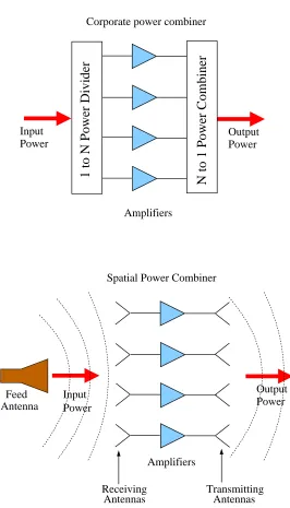
is spread out over a great extent of circuit board area, and hence the power combining losses in transmission lines and combiners become significant and the power combining efficiency drops as the operation frequency increases. The losses in the transmission lines that implement Wilkinson power dividers or any other couplers also dictate an upper limit to the number of solid state devices that can be used to combine power.
Corporate power combiner
Feed Antenna
1 to N Power Divider N to 1 Power Combiner
Input Power
Output Power
Amplifiers
Output Power Spatial Power Combiner
Transmitting Antennas Receiving
Antennas
Amplifiers Input
Power
shown in figure 1.2. The power combining takes place in free space or inside a low-loss overmoded waveguide without the need for power splitters or di-viders as in corporate power combiners and hence the losses in the combining structure are minimized. One can either radiate the combined power directly into free space, or collect the combined power with an antenna similar to the input feed antenna and form a conventional two port power amplifier. Spa-tial power combiners have the additional advantage over the vacuum tubes that the failure of a few active devices does not mean a catastrophic failure at system level as will be shown later in this dissertation. As spatial power combining systems continue to achieve higher power levels at microwave and millimeter wave frequencies after a decade of development, recent research on spatial power amplifiers has concentrated on increasing the power output levels, power added efficiencies and power combining efficiencies of the exist-ing systems. Accurate electromagnetic modelexist-ing of spatial power combiners has therefore become essential. However, analysis of spatial power combin-ers has been a challange for the designcombin-ers due to their electromagnetically large structure. A typical spatial power combiner array is a few wavelenghts in length and width, and a typical feed antenna can be three to ten wave-lengths. The array elements on the other hand can be very small in size with respect to the whole system, which introduces additional difficulty in the discretization process for the numerical methods.
Up until now, the design procedure of spatial power combiners has been through the unit cell approach, where each element of the power combining array consisting of the transmitting and receiving antennas and an active device is modeled individually. In this approach, one may assume an infinitely periodic structure and make use of electromagnetic symmetry by establishing electric and magnetic side-walls for the unit cell. As a result one neglects the effects of mutual coupling among the unit cells. Furthermore, if the spatial power combiner/divider is waveguide-based, the effects of the metal side walls are neglected in addition to the fact that the array is assumed to be infinite.
be modeled. Another objective is to investigate the effects of different array parameters on the performance of the spatial power combining system and optimize these parameters for the increased power combining efficiency.
In this dissertation, the GSM approach is utilized in order to model a waveguide-based spatial power combiner. The approach combines FDTD (Finite Difference Time Domain) and MM (mode matching) techniques in order to predict the system behavior. It is important to break the electro-magnetically large system into smaller blocks, since each individual block can be simulated by using the most suitable and most efficient numerical technique. With the tools to be developed in this dissertation, a designer should be able to have a better understanding of the physics in spatial power combiners and design for increased power combining efficiency.
1.2
Dissertation Overview
Chapter 2 gives a brief retrospect of spatial power combining and reviews different spatial power combining techniques. A brief introduction to and recent advances in FDTD (Finite Difference Technique) will also be presented in this chapter.
Chapter 3 introduces a modified unsplit PML (perfectly matched layer) implementation for use in absorbing evanescent modes as well as propagating modes in oversized inhomogeneous or homogeneous waveguides. This imple-mentation is based on the stretched coordinate modification of Maxwell’s equations.
Chapter 4 presents the details of a revised mode matching algorithm for calculating the GSM of double step waveguide junctions between two dielectric loaded waveguides, or between a hollow and a dielectric loaded waveguide. This algorithm is used to analyze and design hard horn feeds or optimized stepped waveguide transformers for spatial power combiners.
Chapter 5 focuses on the details for the FDTD simulation of coax-fed patch antenna arrays inside oversized and dielectric loaded waveguides.
Chapter 6 validates the simulation results for a passive spatial power combiner system with experimental data. Investigation of design parameters for different sized arrays is also presented along with a device failure analysis for an already built aperture coupled 5×5 patch array.
In Chapter 7, a summary of the dissertation is given along with conclu-sions and suggestions for future work in this topic.
cascading procedure and cascading schematics, respectively.
1.3
Original Contributions
The most important achievements of this work are:
• Simulation of electromagnatically large spatial power combiners by us-ing the generalized scatterus-ing (GSM) approach along with different simulation techniques such as finite element method (FEM), finite dif-ference time domain (FDTD), and mode matching (MM).
• Studying design parameters of spatial power combiner arrays for opti-mizing power combining efficiency and output power levels.
• A device failure analysis on a spatial power amplifier that was developed and built earlier.
• Improving the existing unsplit perfectly matched layer absorbing bound-aries in FDTD to absorb evanescent modes in waveguides.
• Transformation between different modal bases in hollow rectangular waveguides and dielectric loaded rectangular waveguides.
• Revised mode-matching codes for both hollow and dielectric loaded discontinuities.
• Design of stepped waveguide transformers for the excitation of spatial power amplifier arrays.
1.4
Publications
• M. Ozkar and A. Mortazawi, “Analysis and design of an inhomogeneous transformer with hard walled waveguide sections,” IEEE Microwave
and Guided Wave Letters, Vol. 10, pp. 55-57, February 2000.
• M. Ozkar and A. Mortazawi, “An inhomogeneous waveguide trans-former with hard walls for the excitation of quasi-optical amplifiers,”
IEEE Antennas and Propagation Society International Symposium, Vol.
• M. Ozkar, S. C. Ortiz, A. B. Yakovlev, A. Mortazawi, and M. B. Steer, “Spatially combined fault tolerant masthead power amplifiers,” IEEE
Topical Workshop on power amplifiers for wireless communications, La
Jolla, California, 11-12 September, 2000.
• M. Ozkar, G. Lazzi, and A. Mortazawi, “Study of design parame-ters in waveguide-based spatial power combining amplifier arrays using FDTD,” IEEE MTT-S International Symposium, 2001.
• M. Ozkar and A. Mortazawi, “An investigation on the effects of the array parameters on the performance of spatial power amplifiers with hard horn feeds,” IEEE MTT-S International Sympoisum, 2002.
• S. C. Ortiz, M. Ozkar, A. B. Yakovlev, M. B. Steer and A. Mortazawi, “Fault tolerance analysis and measurement of a spatial power ampli-fier,” IEEE MTT-S International Symposium, 2001.
• A. Mortazawi and M. Ozkar, “Hard horn feeds for quasi-optical ampli-fiers,” XXVIth URSI General Assembly Meeting, 1999.
• A. I. Khalil, M. Ozkar, A. Mortazawi, and M. B. Steer, “Modeling of waveguide-based spatial power combining systems,” IEEE Antennas
and Propagation Society International Symposium, Vol. 4, pp.
2374-2377, 1999.
• A. B. Yakovlev, S. C. Ortiz, M. Ozkar, A. Mortazawi, and M. B. Steer, “A waveguide-based aperture-coupled patch amplifier array: Full wave analysis and experiment,” IEEE Transactions on Microwave Theory
and Techniques, Vol. 48, pp. 2693-2699, December 2000.
• A. B. Yakovlev, S. C. Ortiz, M. Ozkar, A. Mortazawi, and M. B. Steer, “Electromagnetic modeling and experimental verification of a complete waveguide-based aperture coupled patch amplifier array,” IEEE
MTT-S International MTT-Symposium, Vol. 2, pp. 801-804, 2000.
• A. B. Yakovlev, S. C. Ortiz, M. Ozkar, A. Mortazawi, and M. B. Steer, “Electric dyadic Green’s functions for modeling resonance and coupling effects in waveguide-based aperture-coupled patch arrays,” IEEE
Literature Review
2.1
Spatial Power Combining
The outputs from a collection of transistors or diodes can be combined at the chip level, in a circuit structure or in free space as it was mentioned in the previous chapter. Spatial power combining refers to combining power from active devices in free space and was reported as early as 1968 [5]. The two terms, quasi-optics and spatial power combining get used interchangeably even though the quasi-optical approach is a variation of combining in free space (spatial power combining). A distinguishing feature of quasi-optical approach is that it employs elements originally developed for optical fre-quencies such as Fabry-Perot cavities and polarizers for combining power. The word quasioptics actually refers to the propagation of a beam of radia-tion that is reasonably well collimated but has relatively small dimensions in terms of wavelengths, transverse to the axis of propagation [6]. In this sense, quasioptics dates back to the earliest experimental studies of radio waves carried out by Heinrich Hertz. Quasi-optical power combining in millimeter-wave to sub-millimeter-millimeter-wave range started in 1986 [7]. From then on, active devices with grid arrays quickly gained interest due to their convenient unit cell based design, the ease planar fabrication and the possibility of mono-lithic construction [8]. Different kinds of active grids include phase shifters [9], multipliers [10], oscillators [11] and mixers [12]. The first monolithic 6×6 grid oscillator array was reported in 1992 [13]. The first demonstration of a grid amplifier was reported by Kim et. al [14]. The 5x5 grid array produced a gain of 11 dB at 3.3 GHz with 50 MESFET devices. Other oscillators and amplifiers that utilize the concept of placing larger grid structures in the far
field of a transmitting antenna followed [15,16,17,18,19] and the first power measurement on a monolithic amplifier at 40 GHz was reported by Rutledge et. al [20].
One of the major problems with the grid structures is the confinement of the radiated beam. This problem can be overcome by combining the power in a guided structure such as a waveguide or a coaxial TEM line [21] or by placing the active array in close proximity of a horn antenna [22]. In [21], a broad band design is achieved by the use of tapered slot lines (vivaldi antennas) as the receiving and transmitting array elements. Further investigations showed that the use of hard horns improved the output power due the uniform excitation of the array elements [23].
Overall, spatial power combiners can be classified in two different cat-egories in terms of their architecture [24]: the tile approach and the tray approach. In the tile approach, the active devices are placed at a plane parallel to the face of the antenna array. There are usually two layers (for dividing and combining power), both of which might include active devices. One has to be able to couple the power from one layer to the other in an efficient manner (usually through slots). In the other approach, known as the tray approach, active devices are placed at a plane that is perpendicular to the face of the antenna array which may consist of vivaldi antennas [21] or aperture coupled patch antennas [25].
waveguide-based spatial power combining arrays using the GSM (General-ized Scattering Matrix) approach as well [31,32]. GSM approach suits well to the waveguide problems since the complexity is reduced by partitioning the system into smaller blocks that can be simulated using different numerical techniques. However, work on simulations that show fundamental under-standing of spatial power combiners has been very limited [33]. Issues that have not been previously addressed are the modeling of spatial power com-bining arrays inside dielectric loaded oversized waveguides, optimization of array parameters (such as inter-element spacing) for higher power combining efficiency, the effects of the waveguide walls and the hard horn dielectric on the array behavior (bandwidth and driving point impedances of the array elements).
2.2
Finite Difference Time Domain (FDTD)
The FDTD method, first published in 1966 [34], is a simple and yet powerful way to solve the differential form of Maxwell’s equations in time domain. Even after 30 years, its usage continues to grow with the increasing computing power. The number of publications in FDTD started to grow especially after the introduction of an effective absorbing boundary condition called perfectly matched layer (PML) by Berenger [35].
In a source free region, the two of the Maxwell’s equations in time domain become:
∇ ×E~ =−µ∂ ~H
∂t (2.1)
∇ ×H~ =²∂ ~E
∂t (2.2)
These two vector equations yield 6 scalar equations which can be discretized in both time and space.
∂Ex ∂t = 1 ² µ ∂Hz ∂y − ∂Hy ∂z ¶ (2.6) ∂Ey ∂t = 1 ² µ ∂Hx ∂z − ∂Hz ∂x ¶ (2.7) ∂Ez ∂t = 1 ² µ ∂Hy ∂x − ∂Hx ∂y ¶ (2.8) (2.9)
The scalar equations can be discretized by spacing E and H fields by half a cell inside a volume, and by half a time step in time using the central differencing scheme. Usually, since the truncation is done in terms of electric fields, one should end the outer boundaries of the region with electric field components as shown in figure 2.2, which is a two dimensional cut of a discretized volume.
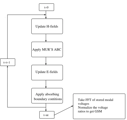
A general flow diagram of the simplest FDTD approach is shown in figure
2.3. The simulation starts with the initialization of all the E and H field components. Including a source is possible by forcing the fields at the source point/region. Different kinds of source implementations will be discussed in one of the following subsections. Whether E or H gets updated first depends on the source. If the source is implemented in terms of H field components, then one should start by updating E-fields first and vice versa. The stability of FDTD is dependent on the choice of the time step, ∆t:
∆t ≤ 1
c0
q 1 ∆x2 +
1 ∆y2 +
1 ∆z2
(2.10)
The value on the right of equation 2.10 is usually referred to as the Courant number. A very common choice of the time step assuming ∆x= ∆y= ∆z = ∆ to ensure stability is:
∆t= ∆
2c0 (2.11)
x
z
y
E E
E E
E
E E
E
E
E
E
E H
H H
H
H
H
z z
z z
z
z x
x
x
x x
x y
y
y y
y y
(i,j,k)
(i-1,j,k)
(i,j+1,k) (i,j,k+1)
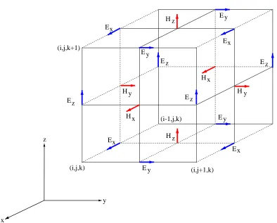
Figure 2.1: Three dimensional Yee cell.
2.2.1
Absorbing boundaries
Simulation of physical problems with unbounded space is impossible without grid truncations due to the large memory and cpu time requirements. For this reason, truncation methods had to be developed for numerical techniques (such as FDTD or FEM) that divide the simulation environment into grids or meshes. One can introduce the artificial boundary conditions that surround the simulation environment such that open space is modeled as accurately as possible. Hence, one can also refer to the grid truncations as absorbing boundary conditions.
be-Ez Ez Ez
Hx Hx
Ey Ey
Ey Ey
Ey Ey
Ez Ez Ez
x
z
y
Hx Hx
(i,j,k) (i,j,k+1) (i,j,k+2)
(i,j+1,k) (i,j+2,k) (i,j+1,k+1) (i,j+2,k+1) (i,j+2,k+2) (i,j+1,k+2)
Figure 2.2: Two dimensional view of FDTD meshes.
hind the methods in the second category is the introduction of an artificial non-physical media which can absorb the incoming waves. These methods allow one to absorb any scattered fields independent of the incident angle. The major disadvantage of material absorbing boundaries is the addition of extra grids to implement the material and hence the addition to the mem-ory requirement. However, they are ideal for open space problems where scattering can occur in any direction. Some of the different techniques for implementing absorbing boundaries will be reviewed in the next chapter, where a modified absorbing boundary implementation is also presented.
2.2.2
Source implementation
t=nt t=0
Update H-fields
Apply MUR’S ABC
t=t+1
Take FFT of stored modal voltages
Normalize the voltage ratios to get GSM Update E-fields
boundary contitions Apply absorbing
Figure 2.3: A general flow diagram of the FDTD algorithm.
The second model is implemented by adding the source fields to the already calculated fields and is usually referred to as the soft source or the additive source.
Depending on the application, both types of sources are commonly used. One clear distinction between the two source models is the fact that a hard source reflects from the waves that might get reflected back from various obstacles in the FDTD volume, while a soft source is transparent to any incoming reflections of such sort.
can readjust for this remaining field value at the new update equation of the source.
Sources can be implemented as any function of time depending on the application. Single frequency (sinusoidal) excitations in FDTD are possible, but one has to run the simulation until steady state is reached unless tran-sients are of interest. Single frequency excitation is usually not the preferred excitation since the real power of FDTD emerges when the system response for a range of frequencies can be determined from a single run. A common function that is used in FDTD source implementations is the Gaussian pulse since it covers a wide range of frequencies starting from dc. With y(t) being the excitation function and t1 being the pulse width (defined as the dura-tion from t= 0 to the point where the function reaches 1/eof its maximum amplitude), a Gaussian pulse as a function of time is expressed as:
y(t) =e−
³
t t1
´2
(2.12)
One can also use a sinusoidally modulated Gaussian pulse to obtain a certain range of frequencies centered around one frequency point:
y(t) =e−
³t−t
0
t1
´2
sin [2πf(n∆t−t0)] (2.13) where f is the center frequency, t1 = 1
2×bandwidth (the pulse width), and
t0 = 4t1 (t0 being the time where the peak of the pulse occurs). The (double sided) bandwidth and the center frequency together determine the range of frequencies that would be of interest in a particular FDTD simulation.
2.2.3
Processing data
Since FDTD is a time domain technique and frequency domain data is almost always the main interest in designing microwave circuits, the time domain data from FDTD simulations needs to be converted to the frequency domain. This can be achieved through Fourier transform, which is given by [40]:
F(fi) =
Z T
0
F(t)e−j2πfitdt (2.14) The above integral can be written in discrete form as:
F(fi) = NX−1
n=0
= NX−1
n=0
F(n∆t) cos(2πfin∆t)−j
N−1 X
n=0
F(n∆t) sin(2πfin∆t)
where F(t) can be any time domain function (fields, voltages) that is cal-culated from FDTD update equations, F(fi) is the Fourier transform of the
F(t) evaluated at the frequency fi, N is the total number of discrete time steps, n is the current time step index, T is the total time over which the FDTD simulation is carried out, and fi is the frequency at which the Fourier transform of F(t) is evaluated. The integral limits should actually extend from negative infinity to positive infinity, but since the signal is causal and the signal is assumed to vanish for t > T, the limits of the integral become 0 toT. This implementation of the Fourier transform is known as the discrete Fourier transform (DFT). DFT can be convenient in most cases, since it can easily be implemented during the time stepping of the FDTD algorithm without any storage requirements.
Another way to perform the Fourier transform is through Fast Fourier Transform (FFT). In this case, the field values that need to be converted to the frequency domain will have to be stored at each time step. It is usually good practice to perform a windowing and zero-padding of the time domain vectors that are stored during the simulation before FFT algorithm is ap-plied to them [41, 42]. Zero-padding in time domain increases the frequency domain resolution due to the increased number of time points and the time domain windowing reduces the aliasing effects if the time domain signal did not completely die out at the end of the FDTD simulation.
2.2.4
Dispersion relations in FDTD
The numerical phase velocities that result in FDTD simulations may differ from the physical phase velocities due to the grid discretization. The ana-lytical dispersion relation for a plane wave in a continuous lossless medium is given by:
ω2µ0²0 =kx2+k2y+kz2 (2.15) where kx,ky and kz are the wavenumbers along x, y,z, respectively. On the other hand, as shown in [36], the same dispersion relation in FDTD is:
µ0²0
∆t [sin(0.5ω∆t)]
2 = · 1
∆xsin(0.5k
0 x∆x)
¸2
+
·
1
∆ysin(0.5k
0 y∆y)
¸2
+
·
1
∆z sin(0.5k
0 z∆z)
¸2
wherekx0,k0yandkz0 are the numerical wavenumbers alongx,y,z, respectively. In the limit where ∆x, ∆y, and ∆z all go to zero, the FDTD dispersion relation becomes the same as the analytical one. The dispersion equation for a hollow rectangular waveguide problem can be obtained by letting k0z =βz
(propagation constant of a particular mode), kx0 = mπX and k0y = nπY with
X and Y being the rectangular waveguide dimensions, m and n being the mode indices andz being the direction of propagation. Details on waveguide dispersion in FDTD implementation can be found in [43, 44].
2.3
Summary
Absorption of Evanescent
Waves in FDTD based on a
Modified Unsplit PML
Formulation
Waveguide problems can be solved by the well known generalized scattering matrix (GSM) technique [45,46]. The idea behind this technique is to break the electromagnetic problem into smaller blocks and to solve each of these blocks by using the most suitable analysis technique such as method of mo-ments (MoM), finite element method (FEM), finite difference time domain (FDTD) or mode matching (MM). The procedure of cascading blocks gener-ally makes use of the frequency domain scattering matrices of each block and this is quite convenient for the frequency domain techniques (MoM, FEM, and MM). On the other hand, FDTD simulations give the response of the system due to a time domain excitation (that might have a spectrum of fre-quency components) in terms of total fields in time domain. In order to use FDTD with other frequency domain techniques in the GSM approach for waveguide problems, one has to be able to extract the frequency domain modal information from the total fields in the time domain correctly. For this purpose, an absorbing boundary that works for all frequencies, regard-less of the modes being propagating and/or evanescent, is needed. With this absorbing boundary, one can define waveguide ports (where the modal information is obtained) and/or make the computation volume limited in the numerical implementation of semiinfinite or infinite waveguides. In this
work, a new absorbing boundary formulation for overmoded waveguides is developed. The new absorbing boundary formulation provides absorption for both evanescent and propagating waves in a waveguide for all frequencies.
If the wave guiding structure is overmoded and the field distribution is changing with frequency, absorbing boundaries such as Mur’s absorbing boundary conditions (ABC) and retarded time absorbing boundary condi-tions (RTABC) fail since the total field cannot be absorbed due to the differ-ent propagation constants of individual modes. Alternatively, one can use the modal absorption technique as presented in [47]. However, even in this tech-nique the problem of absorbing modes whose field distribution change with frequency remains to be addressed. The most suitable absorbing boundary condition for absorbing fields that propagate in overmoded guided struc-tures and that vary with frequency is the perfectly matched layer (PML). PML was originally developed for terminating free space simulations as re-flectionless absorbing boundary for all frequencies, all polarizations and all angles of incidence. However, previous studies have shown that the original PML developed by Berenger is not very effective in absorbing evanescent waves [48, 49, 50, 51]. Recently more research has been directed towards absorbing boundaries for evanescent waves to be used in FDTD simulations [52,53, 54, 55,56].
Evanescent modes play an important role in the cascading of closely spaced waveguide blocks and have to be included in the cascading proce-dure if the waveguide ports are not far enough from the discontinuities for the evanescent modes to die out. The aim of this chapter is to provide a crit-ical review of the currently available techniques for waveguide termination in FDTD and to introduce a modified version of the unsplit PML for use in the FDTD simulations of overmoded waveguide problems.
3.1
Review of Absorbing Boundary
Condi-tions (ABCs) in FDTD
propagat-ing waves with no additional FDTD meshes, however, prior knowledge about how the wave propagates is necessary. The second category ABCs on the other hand do not need any information about the propagation of the waves, but they require additional memory due to the additonal FDTD meshes for the implementation.
Mur’s absorbing boundary conditions
Mur’s ABCs which fall into the first category of ABCs described earlier, were developed in [57]. This was based on the formulation by Engquist and Majda [58] for computer simulation of wave equations.
For the first order Mur’s ABC, the update equation forEz component is discretized as follows for absorption in the x direction:
Ezn+1(0, j, k+ 1/2) = Ezn(1, j, k+ 1/2) + c0∆t−∆x
c0∆t+ ∆x
h
Ezn+1(1, j, k+ 1/2)
− Ezn(0, j, k+ 1/2)
i
(3.1)
where the discretization scheme in figure 2.2 has been used.
As mentioned in [59], the potential problem with Mur’s ABCs is the fact that the error increases with the increasing number of time steps. Neverthe-less. as long as the step size is comparable to the wavelength (∆z ≈ 10λ), accurate results can be obtained from Mur’s ABCs in general. However, it becomes impractical to use Mur’s ABCs if the step size is much smaller than the wavelength.
Retarded time absorbing boundary conditions
This type of ABC falls into the first category of ABCs described previously and was developed by Berntsen and Hornsleth [60]. It is based on the fol-lowing principles:
• Ift = 0 is a time such that the wave arrives at the boundary at a time larger than t = 0, the field calculated by any numerical method with vanishing boundary field represents an outgoing wave for t≤0.
• Based on Huygen’s principle, the outgoing field at time t at a distance h from the boundary is generated by the boundary field at retarded times.
• If the field at the boundary y = 0 is outgoing for times less than tn, the field at y=h will be outgoing for times less thantn+c0h
The retarded time absorbing boundary condition, RTABC, can easily be integrated into the FDTD algorithm since it only requires the knowledge of the field points at previous time points directly adjacent to the computational domain. Choosing the time step, ∆tas 0.5
³ ∆
c0
´
, theEx update equation for an RTABC aty = 0 can be written as (using the same discretization scheme as in figure 2.2):
Exn+2(i,0, k) =Exn(i,1, k) + 0.5 [Exn(i,0, k)−Exn(i,2, k)] (3.2) +Exn+1(i,1, k)−Exn−1(i,1, k)
In 1D formulation, the Ex field update equations for an RTABC at z = 0 can be expressed as simple as:
Perfectly matched layer
PML was first proposed by Berenger in 1994 [35]. The original formula-tion was in 2D, but it was shown that it works for 3D as well [61]. Many other publications have appeared since then on improving this method of absorption [62, 63, 64]. As of today, it is a widely used absorbing boundary condition for FDTD. The idea behind PML is the introduction of an artifi-cial material in order to absorb the outgoing waves. Hence, it is a material based absorbing boundary condition. The original formulation consisted of splitting each field component into two subcomponents. However, as Sulli-van pointed out, PML can be implemented without the need for splitting the field components as well [65]. More details will be given about the unsplit PML implementation in the later sections. If σ and σ∗ denote the electric conductivity and magnetic loss assigned to an outer boundary layer to absorb outgoing waves, respectively, it is well known that
σ ²0 =
σ∗
µ0 (3.4)
maintains reflectionless transmission of a plane wave propagating normally across the interface between free space and the outer boundary layer.
The two curl equations of Maxwell can be modified and be written in terms of 12 equations by splitting each of the six Cartesian field vectors into two as follows [61]:
µ0∂Hxy ∂t +σ
∗
yHxy =−
∂(Ezx+Ezy)
∂y
µ0∂Hxz ∂t +σ
∗ zHxz =
∂(Eyx+Eyz)
∂z
µ0∂Hyz ∂t +σ
∗
zHyz =−
∂(Exy+Exz)
∂z
µ0∂Hyx ∂t +σ
∗ xHyx =
∂(Ezx+Ezy)
∂x
µ0∂Hzx ∂t +σ
∗
xHzx =−
∂(Eyx+Eyz)
∂x
µ0∂Hzy ∂t +σ
∗ yHzy =
∂(Exy+Exz)
∂y
²0∂Exy ∂t +σ
∗ yExy =
∂(Hzx+Hzy)
²0∂Exz ∂t +σ
∗
zExz =−
∂(Hyx+Hyz)
∂z
²0∂Eyz ∂t +σ
∗ zEyz =
∂(Hxy +Hxz)
∂z
²0∂Eyx ∂t +σ
∗
xEyx =−
∂(Hzx+Hzy)
∂x
²0∂Ezx ∂t +σ
∗ xEzx=
∂(Hyx+Hyz)
∂x
²0∂Ezy ∂t +σ
∗
yEzy =−
∂(Hxy +Hxz)
∂y
An additional degree of freedom is introduced with the splitting of the field components. This modification allows the specification of a lossy material layer such that a planar interface between the PML material and the free space is reflectionless for all frequencies, polarizations, and angles of inci-dence. The conductivity profiles are usually of the form:
σ(ρ) =σm
³ρ
δ
´n
(3.5)
where ρ is any one of the x, y and z coordinate variables and δ is the PML thickness. The conductivity profiles can be optimized and modified in order to provide better performance [66]. For most purposes, however, equation
3.5 will provide sufficient absorption.
As for discretizing the 12 field equations presented earlier, one cannot use the standard Yee time-stepping since the attenuation of the outgoing waves is rapid. Therefore, as suggested by Berenger, one can use an explicit expo-nentially differenced time advance. As an example, the Ey field component update equation in 2D case for absorption in x direction can be written as:
Eyn+1
i,j+1/2 = e −σ∆t
²0 Eyn
i,j+1/2
+ 1
σ∆x
³
e−σ²∆0t −1
´ ³
Hzn+1/2
i+1/2,j+1/2 −H n+1/2 zi−1/2,j+1/2
´
Modal absorption
there are not too many higher order modes, modal absorption seems to be the best solution to truncate waveguide simulations since it does not require any additional layers of cells to be simulated. The continuity for each mode is established by obtaining the impulse response (propagation characteristics) of each mode and then making use of convolution.
H z y
x
z
E
E x
y
(i,j,k) (i+7,j,k)
(i,j+6,k)
z=z0
Y
Rectangular Waveguide
X
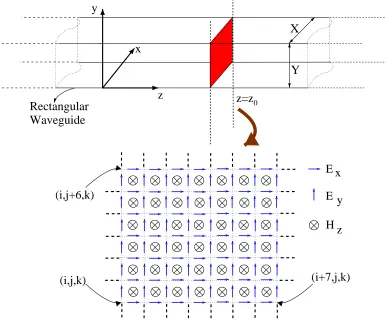
Figure 3.1: Coordinate system for the calculation of modal voltages and the location of the E and H fields at a transverse plane in a homogeneous waveguide .
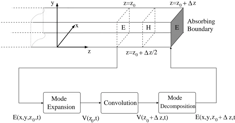
At a given transverse plane, the total electric field in a rectangular waveg-uide with the coordinate system shown in figure 3.1 can be represented in terms of modal voltages, Vs, as follows:
~
E(x, y, z0, t) = N
X
s=1
where~es is the modal field vector for modes. For homogeneous waveguides, the modal field vector is only dependent on the transverse space coordinates and hence the above equation holds in both time domain and frequency domain. For inhomogeneously filled waveguides (such as partially dielectric loaded waveguides), the modal field distribution may depend on frequency and therefore the above equation no longer holds and needs to be modified into a convolution equation in time domain. For T Ez and T Mz modes in the homogeneous rectangular waveguide with the coordinate system in figure
3.1, the modal vectors are given by:
~eTEmn (x, y) = eT Ex (x, y) ˆax+eT Ey (x, y) ˆay
=
"³² 0m²0n
XY
´1
2 Kyn
p
Kxm2 +Kyn2 cosKxmx sinKyny
#
ˆ
ax
−"³²0m²0n
XY
´1
2 Kxm
p
Kxm2 +Kyn2 sinKxmx cosKyny
#
ˆ
ay(3.7)
~eTMmn (x, y) = eT Mx (x, y) ˆax+eT My (x, y) ˆay
= −
"³² 0m²0n
XY
´1
2 Kxm
p
Kxm2 +Kyn2 cosKxmx sinKyny
#
ˆ
ax
−"³²0m²0n
XY
´1
2 p Kyn
Kxm2 +Kyn2 sinKxmx cosKyny
#
ˆ
ay(3.8)
where X and Y are the waveguide width and height respectively and
Kxm =mπ X Kyn =nπ Y
²0p =
½
1 p = 0
2 p 6= 0 p = m or n (3.9)
One should note that the modal vector representations given here are not normalized by power. The normalization process will be explained later. One can calculate the modal amplitudes at the transverse plane located at
z =z0 from the total field using orthogonality between modes as follows:
Vs(z0, t) =
Z Z
~
where the surface integral is over a transverse plane atz =z0 as in figure3.1. It is also possible to define modal currents in terms of H~ fields and h(x, y~ ) modal vectors, but as shown in [44], the best way to implement a modal absorbing boundary is by using the modal voltages if truncation of the time domain signal is to be used.
The algorithm for the modal absorption is demonstrated in figure 3.2. The idea is to know in advance what the transverse electric field values are going to be at the termination plane at a current time step of FDTD. Since the impulse response of any mode for propagation can be calculated in advance as will be shown later in this section, it is possible to perform a convolution operation on the modal voltages found from equation3.10(modal expansion) and obtain the modal voltages at the current FDTD time step at another transverse plane. In this case, the other transverse plane becomes the absorbing boundary once the transverse electric field components are updated using equation 3.6 (modal decomposition).
The integral of equation 3.10 can be discretized by assuming a constant value for the modal field vector components (Ex and Ey) over the FDTD grid and approximating the integral by a double summation [44]. A more accurate discretization would be by taking out the constant values for the total field vector components from one of the integrals and keeping the other integral. This way, the double integral is approximated by one summation and one integral.
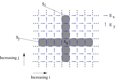
The double integral on the right side of equation3.10 can be written as a summation of double integrals over rows and columns of FDTD grids at the transverse plane. Expanding the dot product in equation 3.10 and dropping the space coordinates and the time dependence for simplicity the following integral is obtained:
Vs(t) =X i
Z
Si
Exex(x, y)dxdy+X j
Z
Sj
Eyey(x, y)dxdy (3.11)
where the integrals are over the surface areas shown as gray columns in figure
3.3. Furthermore, the modal vector components ex and ey of equations 3.7
and 3.8 can be written as a multiplication of a constant (Cx or Cy), an x
dependent function and a ydependent function for bothT E andT M modes in a hollow rectangular waveguide:
ex(x, y) =Cxφx(x)φx(y)
0
z=z
0+ ∆z/2
z=z
0
z=z + ∆z
0 V(z ,t) 0
E(x,y,z ,t) E(x,y,z +0 ∆z,t)
0 ∆ y x z Absorbing Boundary Mode Convolution Expansion Mode E H
V(z + z,t)
Decomposition
E
Figure 3.2: Basic algorithm for modal absorption.
Substituting these into equation3.11, one obtains:
Vs(t) = X i
Cx
Z
Exφx(y)dy
Z
φx(x)dx
+X
j
Cy
Z
Eyφy(x)dx
Z
φy(y)dy
The second integral terms inside the summations R φx(x)dx and R φy(y)dy, are straightforward to evaluate since both φx(x) and φy(y) are explicitly known for hollow rectangular waveguides. The first integral terms inside the summations can be evaluated as follows:
Z
Exφx(y)dy = X j
Z
Sij
Exφx(y)dy
= X
j ∆y
2 [Ex(j)φx(j) +Ex(j−1)φx(j−1)]
Z
Eyφy(x)dx = X i
Z
Sij
Eyφy(x)dx
= X
i ∆x
E
E
x
y
Si
Increasing j
Increasing i
Sj
Sij
Figure 3.3: Surface areas for the integrals of equation 3.11.
Thus a more correct way of numerical integration for equation3.10is achieved compared to the double summation approximation in [44].
By expressing the total field in terms of its modal voltages as in equation
3.10, one can reduce the 3D problem into 1D problem for each mode. The second order differential equation in 1D that represents waveguide propaga-tion in terms of modal voltages [54]:
∂2Vs ∂z2 −
1
c20 ∂2Vs
∂t2 −k
2
c,sVs= 0 (3.12)
which can easily be discretized as:
Vst+1(k) = c
2∆t2
∆z2
£
Vst(k+ 1)−2Vst(k)−Vst(k−1)¤
is given by [67]:
∆t≤ 2
c0
q
kc,s2 +¡∆2 z
¢2 (3.14)
The time step in equation3.14is greater than the Courant number for the 3D FDTD with the same space grid, and therefore the 1D equation can be run in parallel with the 3D FDTD update equations. This saves a considerable amount of computational time in homogeneous waveguide simulations [47].
The main usage of the 1D line equation for waveguides, however, is to cal-culate the waveguide impulse response and to use this response to provide a continuity for the wave as it is demonstrated in [54]. In order to calculate the impulse response, a four node transmission line can be solved using equation
3.13with the excitation of an impulse at the first as an initial condition. Due to the impulse excitation the voltage will propagate in one direction and the voltage read at the second node will be the impulse response of that mode for one discrete step in space. The last two nodes can be used to provide the required termination using a convolution operation with the knowledge of the already calculated impulse response. After the impulse response of the voltage of a particular mode is calculated, the transverse electric fields required to terminate that particular mode at the absorption plane can easily be calculated from equation 3.6.
Once the time domain reflected and transmitted modal voltages at a reference plane are calculated, the frequency domain representations can be obtained through an FFT algorithm. It then becomes possible to calculate the scattering parameters by dividing voltages and normalizing by power. If
P1 and P2 are two waveguide ports as shown in figure 3.4, ands corresponds to the mode index as earlier, the normalized scattering parameters at the waveguide port P1 are given by:
SsP1P1isr = V P1 sr (f)
VsP1i (f) ·
s
ZsP1i (f)
ZsP1r(f) (3.15)
SsP2P1isr = V P1 sr (f)
VsP2i (f) ·
s
ZsP2i (f)
ZsP1r(f) (3.16) where the subscript unders stands for either reflectedr or incidenti modes,
as a function of frequency. Similarly, the normalized scattering parameters at the waveguide port P2 are given by:
SsP2P2isr = V P2 sr (f)
VsP2i (f) ·
s
ZsP2i (f)
ZsP2r(f) (3.17)
SsP1P2isr = V P2 sr (f)
VsP1i (f) ·
s
ZsP1i (f)
ZsP2r(f) (3.18) These definitions can easily be extended for an n port system that can have multiple modes at each port. The formulation presented in this section for calculating modal voltages will be used in the last section of this chapter, where different absorbing boundaries will be compared.
y
x Absorbing
Boundary Absorbing
Boundary
P1 P2
Vs
r P1
z
Vs
i P1
Vs
i P2
V sr
P2
Figure 3.4: Two port waveguide with a discontinuity.
![Figure 1.1: Single device average output power as a function of frequencyfrom various solid state and tube devices [4].](https://thumb-us.123doks.com/thumbv2/123dok_us/1400191.1172700/19.612.132.480.121.466/figure-single-device-average-function-frequencyfrom-various-devices.webp)