Abstract
SUNDARARAMAN, VISHWANATH Development of ASIC technology library for the
TSMC 0.25µm standard cell library (Under the direction of Dr. Paul D. Franzon)
The Synopsys synthesis tool generates the hierarchical netlist of a design using worst-case and best-case ASIC technology libraries. The worst-case library checks for the setup time violation and the best-case library checks for the hold time violations of the design. The worst-case library is characterized by a supply voltage of 2.25V, operating temperature of 125°C, and slow process corner. The best-case library is characterized by a supply voltage of 2.75V, operating temperature of -55°C, and fast process corner. The technology libraries are developed for the CMOS TSMC 0.25µm technology. The CMOS nonlinear delay models are used for delay calculations. Variations in operating temperature, supply voltage and manufacturing process causes performance variations in electronic networks. Using different operating conditions, the timing of the design under different environmental conditions can be evaluated. The delay values specified in the cells for a technology specify a set of nominal operating condition. The worst-case and best-case libraries are developed by running HSPICE simulations for all the 36 basic cells. The technology library contains information used for the following synthesis activities:
Translation – functional information for each cell
Optimization – area and timing information for each cell (including timing constraints on sequential cells)
Development of ASIC technology library for the TSMC 0.25µm standard cell library
by
Vishwanath Sundararaman
A thesis submitted to the graduate faculty of North Carolina State University
In partial fulfillment of the requirements of the degree of Master of Science
COMPUTER ENGINEERING Raleigh
2003 Approved by
________________________________
Dr. Paul D. Franzon, Chair of the Advisory Committee
Biography
Vishwanath Sundararaman was born on 5th April 1980 in Pune, India. He graduated with a B.E (Honors) degree in Electrical and Electronics Engineering from the Birla Institute of Technology and Science (BITS), Pilani, Rajasthan, India in June 2001. He was an intern with Siemens Communication Software at Bangalore, India between January and June 2001.
Acknowledgements
Graduate school at NC State has been a wonderful experience. I take this opportunity to thank the people who enriched the two years that I spent here.
First and foremost, I would like to express my sincere thanks to my advisor Dr. Paul D. Franzon, for his guidance, support, patience and his constant encouragement. Working with him has been a fantastic learning experience. I also thank him for his confidence in me, and for giving me an opportunity to explore a variety of topics.
I would like to thank the other members of my advisory committee, Dr. Eric Rotenberg and Dr. Griff Bilbro, for reviewing my thesis, and for their valuable comments. I would like to thank Dr. Rhett Davis for giving invaluable suggestions, guidance and encouragement. I would like to thank all the other faculty members, for providing me with such an excellent education.
I would like to thank Jos Sulistyo of Virginia Polytechnic Institute and State University for his help in developing the cell library. I would also like to thank Hao Hua for being patient and helping me run simulations whenever I had problems.
Finally, I would like to thank my parents, Dr.Sundararaman and Sundari, for their unconditional love and continual encouragement. I thank them for the active role they played in my education and also guiding me whenever I needed their advice. I cannot thank them enough.
TABLE OF CONTENTS
LIST OF FIGURES ... vii
LIST OF TABLES ... viii
Chapter 1 Introduction... 1
1.1 Organization of the thesis ... 2
Chapter 2 VTVT Standard Cell Library... 4
2.1 Introduction... 4
2.2 Modification to the NCSU kit... 4
2.2.1 Modifications under the directory – techfile... 5
2.2.2 Modifications under the directory – skill... 6
2.3 Cells contained in the Library... 6
2.4 Files for PNR ... 8
Chapter 3 Technology Library... 9
3.1 Introduction... 9
3.2 Developing the Technology library ... 9
3.2.1 Library Group ... 10
3.2.2 General Library Attributes... 10
3.2.3 Delay and Skew Attributes ... 10
3.2.4 Defining Units... 12
3.2.5 Timing Group... 13
3.2.6 Three-State Timing Arcs... 13
3.2.7 Edge-Sensitive Timing Arcs ... 14
3.2.8 Preset and Clear Timing Arcs ... 14
3.3 Delay Model ... 15
3.3.1 CMOS Nonlinear Delay Model ... 15
3.3.2 Delay Model Template ... 15
3.3.3 Cell Delay & Transition Delay ... 16
3.3.4 Setup and Hold time... 18
3.4 Library Compiler ... 18
3.5 Symbol Library ... 19
3.6 Synthesis with Design Analyzer ... 20
3.7 Post synthesis design library... 20
Chapter 4 Verification of the ASIC technology library ... 22
4.1 Introduction... 22
4.2 Checking Library Consistency... 22
Chapter 5 Conclusion and Future Work... 27
5.1 Future Work... 27
5.1.1 Power ... 27
5.1.2 Operating Conditions ... 29
5.1.3 Modeling Wire Load... 30
Bibliography ... 31
LIST OF FIGURES
Figure 3-1: Delay modeling for falling signal. ... 11
Figure 3-2: Skew modeling... 12
Figure 4-1: Simulation waveforms for the 32-bit multiplier. ... 24
Figure 4-2: Layout of the 32-bit multiplier... 25
Figure 4-3: Simulation waveform for IP forwarding engine. ... 26
LIST OF TABLES
Chapter 1 Introduction
The TSMC 0.25µm deep submicron technology cell library was developed by the VTVT (Virginia Tech VLSI for Telecommunication) group. The ASIC technology library for this CMOS TSMC 0.25µm technology is being developed to be used for academic and research purpose at North Carolina State University (NCSU). The ASIC technology library is an extension of the standard cell library developed by J.B. Sulistyo and D.S. Ha [1] of the VTVT group and will be a part of the NCSU cadence design kit (NCSU CDK).
The modifications necessary for the NCSU CDK to support this new deep submicron TSMC 0.25µm technology is provided by the VTVT group. The new technology library is compiled into the NCSU cadence kit along with the modifications required. The TSMC 0.25µm deep submicron cell library contains a total of 37 cells. The layouts of the cells are developed using the modified version of the NCSU kit version 1.1, which uses the MOSIS DEEP design rules.
synthesis using Synopsys synthesis tool. The validity of the library is verified by post synthesis simulation and placement & routing of a test design.
An environment is set for doing “Placement and routing” (PNR) using Cadence Silicon Ensemble. The Library Exchange Format (LEF) file, GDSII map file, used for exporting the result of the PNR tool run to the design framework (dfII) environment, needed for doing place and route is provided by the VTVT group.
Currently, the ASIC technology library is being developed only at NCSU. The NCSU CDK has been downloaded by over 2000 organizations, mostly universities and has won prizes and recognitions from Cadence, NSF and CUG.
In this thesis the Courier New font refers to the different parameters specific to the technology files in the NCSU CDK
and the attributes specific to the ASIC technology library.
The Courier New font words in italics refer to the commands
in the Library Compiler shell interface.
1.1 Organization of the thesis
Chapter 2 VTVT Standard Cell Library
2.1 Introduction
The VTVT group has developed the standard cell library kit based on the TSMC 0.25µm technology. The layouts were developed using a modified version of the NCSU CDK version 1.1, which uses the MOSIS DEEP design rules. The kit, as distributed by the VTVT group, includes the following:
- Modifications to the NCSU CDK to incorporate the new technology - Layouts in GDSII and cadence dfII format
- Library Exchange Format (LEF) file for the PNR tool
The layouts include only simple cells such as two and three input combinational cells, tri-state buffers, flip-flops, and latches. The VTVT standard cell library is intended for use with Cadence Silicon Ensemble placement and routing tool. The layouts were developed with Cadence Virtuoso custom layout tool and the MOSIS DEEP design rules were followed.
2.2 Modification to the NCSU kit
the NCSU kit installation directory. The new technology library is then compiled into the NCSU kit after the required modifications have been performed.
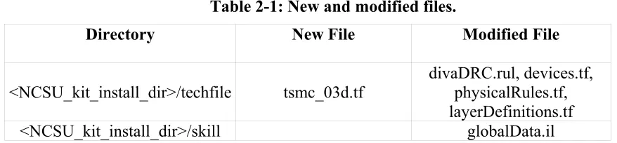
Table 2-1: New and modified files.
Directory New File Modified File
<NCSU_kit_install_dir>/techfile tsmc_03d.tf divaDRC.rul, devices.tf, physicalRules.tf, layerDefinitions.tf
<NCSU_kit_install_dir>/skill globalData.il
2.2.1 Modifications under the directory – techfile
divaDRC.rul
This file is the DRC (design rule check) script of the NCSU kit. Modifications to this file have been made to include the check for DEEP rule violations. In most cases the DEEP and SUBM rules are identical and hence the conditional statement of
“submicronAvailable” is replaced by (submicronAvailable ||
deepAvailable), where the submicronAvailable and deepAvailable are NCSU kit’s flag variables to identify MOSIS SUBM and DEEP rules respectively. For cases where DEEP and SUBM rules are different, new conditional statements such as “if (deepAvailable)” are introduced.
devices.tf
A new variable “deepAvailable” is defined and calculated. The conditional statements using submicronAvailable is replaced by (submicronAvailable
physicalRules.tf
The value of the variable deepAvailable is assigned as
deepAvailable = NCSU_techData[technology] -> deeprules . Various new spacing rules are added for the DEEP rules.
layerDefinitions.tf
A new entry is created for the DEEP version of TSMC 0.25µm technology, using the same values used by the SUBM version of the technology.
tsmc_03d.tf
This file has the description of the DEEP version of the TSMC 0.25µm technology.
2.2.2 Modifications under the directory – skill
globalData.il
A new entry is added for the TSMC 0.25µm technology using the MOSIS DEEP rules. The new entry is called TSMC_CMOS025_DEEP with design scaling unit (lambda) set to 0.12µm. The NCSU_parasiticCapIgnoreThreshold parameter is changed from 2fF to 1aF. This parameter refers to the largest value of the parasitic capacitance that can be ignored during netlist extraction.
2.3 Cells contained in the Library
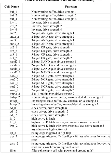
Table 2-2: Cells contained in the standard cell library.
Cell Name Function
buf_1 Noninverting buffer, drive strength 1 buf_2 Noninverting buffer, drive strength 2 buf_4 Noninverting buffer, drive strength 4 inv_1 Inverter, drive strength 1
inv_2 Inverter, drive strength 2 inv_4 Inverter, drive strength 4
and2_1 2-input AND gate, drive strength 1 and2_2 2-input AND gate, drive strength 2 and3_1 3-input AND gate, drive strength 1 and3_2 3-input AND gate, drive strength 2 or2_1 2-input OR gate, drive strength 1 or2_2 2-input OR gate, drive strength 2 or3_1 3-input OR gate, drive strength 1 or3_2 3-input OR gate, drive strength 2 nand2_1 2-input NAND gate, drive strength 1 nand2_2 2-input NAND gate, drive strength 2 nand3_1 3-input NAND gate, drive strength 1 nand3_2 3-input NAND gate, drive strength 2 nor2_1 2-input NOR gate, drive strength 1 nor2_2 2-input NOR gate, drive strength 2 nor3_1 3-input NOR gate, drive strength 1 nor3_2 3-input NOR gate, drive strength 2 xor2_2 2-input XOR gate, drive strength 2 mux2_2 2-to-1 multiplexer, drive strength 2
bufzp_2 Noninverting tri-state buffer, low-enabled, drive strength 2 Invzp_1 Inverting tri-state buffer, low-enabled, drive strength 1 Invzp_2 Inverting tri-state buffer, low-enabled, drive strength 2 cd_8 clock driver, drive strength 8
cd_12 clock driver, drive strength 12 cd_16 clock driver, drive strength 16
lp_2 high-active D latch
lrp_2 high-active D latch with asynchronous low-active reset lrsp_2 high-active D latch with asynchronous low-active reset and
asynchronous high-active set dp_2 rising-edge triggered D flip-flop
drp_2 rising-edge triggered D flip-flop with asynchronous low-active reset
drsp_2 rising-edge triggered D flip-flop with asynchronous low-active reset and asynchronous high-active set
The standard cell library also contains layouts of some dummy pads. These dummy pads are not intended for use with actual designs. They are created only for convenience of creating the LEF file.
2.4 Files for PNR
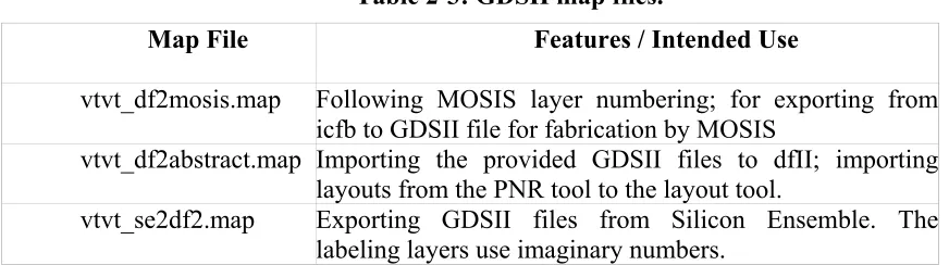
The LEF file is generated for use with Silicon Ensemble. The LEF file includes LEF descriptions of the VTVT standard cells as well as the LEF descriptions of the dummy I/O power and corner cells. Actual pads are not used in creating the LEF descriptions, as their size and complexity result in large LEF descriptions hence dummy pads are used. The verilog template file contains no logic descriptions of the cells. It simply provides a template of the cells (list of input, output, and power pins) needed for the PNR tool. The GDSII map file is used for exporting the result of the PNR to the design framework (dfII) environment. Table 2-3 has a list of GDSII map files developed by the VTVT group.
Table 2-3: GDSII map files.
Map File Features / Intended Use
vtvt_df2mosis.map Following MOSIS layer numbering; for exporting from icfb to GDSII file for fabrication by MOSIS
vtvt_df2abstract.map Importing the provided GDSII files to dfII; importing layouts from the PNR tool to the layout tool.
Chapter 3 Technology Library
3.1 Introduction
The ASIC synthesis libraries have been developed for the TSMC 0.25µm technology as part of this thesis. This chapter provides an overview of the library development and describes the general procedure followed in developing this library [2] [3]. The technology library describes the structure, function, timing, and environment of the ASIC technology. The technology library contains information used in the following synthesis activities.
Translation - functional information for each cell.
Optimization - area and timing information for each cell. Design rule fixing - design rule constraints on cells.
The library development consists of the following major activities. Describing the library in the text format (.lib and .slib). Compiling the binary form of the library (.db or .sdb).
3.2 Developing the Technology library
The library description identifies the characteristics of a technology library and the cell it contains. The technology libraries are developed for both the worst-case, characterized by a supply voltage of 2.25V, operating temperature of 125°C, and slow process corner, and the best-case, characterized by a supply voltage of 2.75V, operating temperature of -55°C, and fast process corner.
3.2.1 Library Group
The library group contains description of the entire library. Attributes that apply to the entire library are defined at the library group level, at the beginning of the library description. The library description for an inverter is attached in Appendix A1 as an example. The library group statement defines the name of the library and is the first executable line in the library.
3.2.2 General Library Attributes
The following attributes generally apply to the technology library.
technology - The technology attribute identifies the technology tool used in the library. The technology attribute is the first attribute defined and is placed at the top of the listing. In this library the technology attribute is the CMOS technology.
delay_model - The delay_model attribute indicates the delay model used in the delay calculations. The delay_model attribute follows the technology
attribute in the library description. The table_lookup (nonlinear delay model) is used in this library.
3.2.3 Delay and Skew Attributes
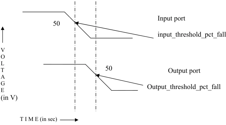
This section describes attributes used to set the values of the input and output pin threshold points. These points are used by the Library Compiler to model delay and skew. output_threshold_pct_fall: This indicates the 50% threshold point
output_threshold_pct_rise: This indicates the 50% threshold point when the output rises from 0 to 1
input_threshold_pct_fall: This indicates the 50% threshold point when the input falls from 1 to 0
input_threshold_pct_rise: This indicates the 50% threshold point when the input rises from 0 to 1
The delay, for example, is the time it takes for the output signal voltage, falling from 1 to 0, to fall to the threshold point (set by the output_threshold_pct_fall
attribute) after the input signal voltage falling from 1 to 0 has fallen to the threshold point (set by the input_threshold_pct_fall attribute) as shown in Figure 3-1.
Figure 3-1: Delay modeling for falling signal.
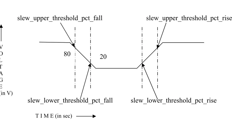
Slew is the time it takes for the voltage value to fall or rise between two designated threshold points on an input or on an output. The following two attributes designate
Input port
input_threshold_pct_fall
Output port
Output_threshold_pct_fall 50
50 V
O L T A G E (in V)
the threshold points to model the transition time for voltage falling from 1 to 0 as shown in Figure 3-2.
slew_lower_threshold_pct_fall : 20.0%
slew_upper_threshold_pct_fall : 80.0%
The following two attributes designate the threshold points to model the transition time for voltage rising from 0 to 1 as shown in Figure 3-2.
slew_lower_threshold_pct_rise : 20.0%
slew_upper_threshold_pct_rise : 80.0%
Figure 3-2: Skew modeling
3.2.4 Defining Units
The Design Compiler tool is unit less. However, units are required to create VHDL libraries and reports. The following library level attributes are specified in the library to define units:
time_unit : "1ps"
20 80
slew_upper_threshold_pct_fall
slew_lower_threshold_pct_fall
slew_upper_threshold_pct_rise
slew_lower_threshold_pct_rise T I M E (in sec)
voltage_unit : "1V" current_unit : "1mA"
pulling_resistance_unit : "1kohm" capacitive_load_unit (1.0, "ff")
3.2.5 Timing Group
The timing group contains information that the design compiler needs in order to model timing arcs and trace paths. Timing arcs are the paths followed by the path tracer during path analysis. The timing group defines the timing arcs through the cell and the relationships between clock and data input signals. The timing group describes the timing relationship between an input and an output pin, timing arcs through a non-combinational element, and setup and holds times on flip-flop and latch inputs. The related_pin
attribute defines the pin that is the starting point of the timing arc. This attribute is a required component of all timing groups.
3.2.6 Three-State Timing Arcs
The three state output pin of a tri-state cell is described by the three-state timing arc. The design compiler uses only the three_state_enable timing arcs. The
three_state_enable timing arc is designated by
The timing_type attribute distinguishes between combinational and sequential cells by defining the type of timing arc, which is three_state_enable for state cells like tri-state inverters and tri-tri-state buffers.
3.2.7 Edge-Sensitive Timing Arcs
Edge sensitive timing arcs from the clock on a flip-flop are identified by the rising_edge on the timing_type attribute. Rising_edge identifies a timing arc whose output pin is sensitive to the rising signal at the input pin. These arcs are path traced, i.e., the path tracer propagates only the active edge path values along the timing arc. The
related_pin attribute is set to the clock input for sequential cells.
3.2.8 Preset and Clear Timing Arcs
Preset timing arcs affect only the rise arrival time on the arc’s endpoint pin while clear timing arcs affect only the fall arrival time. These timing arcs are used for asynchronous reset and clear pins on the flip-flops and level sensitive latches. Accordingly, a rise time is defined for the preset arc and a fall time is defined for the clear arc. The rise time for the preset arc and the fall time for the clear arc are defined by creating a rise delay table and a fall delay table, respectively as defined in Section 3.3.3. For the preset arc, the timing_type attribute is set to preset and for the clear arc, the
3.3 Delay Model
The Design Compiler uses timing parameters and environment attributes described in the technology library to calculate timing delays of the design. The timing parameters and environment attributes used in the timing delay calculations are dependent on the delay model used. The CMOS nonlinear delay model is used in this ASIC technology library.
3.3.1 CMOS Nonlinear Delay Model
The delay value predicted by the Library Compiler and the timing analyzer is enhanced by the CMOS nonlinear delay model. The CMOS nonlinear delay model uses lookup tables and interpolation to compute delays. The model is flexible enough to provide close timing correlation for a wide variety of delay modeling schemes. The nonlinear delay model is characterized by tables that define the timing arcs.
The library level lu_table_template group attribute is used to define templates of common information to use in lookup tables. The lookup tables and the corresponding templates used in this library are two dimensional.
3.3.2 Delay Model Template
3.3.2.1 Template Variables for Timing Delays
The table template (rise_delay_table, fall_delay_table) specifying timing delays have two variables. The variables indicate the parameters used to index into the lookup table along the first and second table axes. The parameters are the input transition time and the output loading.
3.3.2.2 Template Variables for Load-Dependant Constraints
The table template (constraint_table) specifying load-dependant constraints have two variables. The variables indicate the parameters used to index into the lookup table along the first and second table axes. The parameters are the input transition time of the constrained pin and the input transition time of the related pin.
3.3.2.3 Template Breakpoints
The index statements in the lookup tables define the breakpoints for an axis. The breakpoints defined by index_1 correspond to the parameter values indicated by variable_1 in the lu_table_template group. The breakpoints defined by index_2 correspond to the parameter values indicated by variable_2 in the
lu_table_template group.
3.3.3 Cell Delay & Transition Delay
cell_rise: This specifies the delay time for an output rise with respect to the input transition. The input pin is specified by the related_pin attribute.
cell_fall: This specifies the delay time for an output fall with respect to the input transition. The input pin is specified by the related_pin attribute.
Transition delay is the time required for the output pin to change state. It is also used to index into delay and transition tables at the next logic stage. Transition delay can also be constrained as a design rule during synthesis. It is a function of both output loading and input transition time. Two groups in the timing group define transition delay tables
rise_transition: This specifies the transition time for an output rise. fall_transition: This specifies the transition time for an output fall.
3.3.4 Setup and Hold time
Setup time is defined as the time for which the data input of a sequential cell should be constant before the active edge of the clock or the enable input. Hold time is defined as the time for which the data input of a sequential cell should be constant after the active edge of the clock or the enable input. Two groups in the timing group define the setup (hold) time.
rise_constraint: This specifies the setup (hold) time for an output rise. fall_constarint: This specifies the setup (hold) time for an output fall.
The constraint pin is the input pin of the sequential cell whereas the related pin is the clock/enable input. The setup and hold times are characterized using bisection in HSPICE [4].
3.4 Library Compiler
files are used in the synthesis of a design using the Synopsys Design Analyzer as explained in section 3.6.
3.5 Symbol Library
The symbol libraries contain information that the design vision tools use to generate and display the graphic representation of the design. The construction of symbol library is technology-independent. The symbol library for the TSMC 0.25µm technology is very similar to the 0.8µm cmosx symbol library currently used here at NC State University. The 0.8µm cmosx symbol library is modified for use with the 0.25µm technology. The symbol library shares the same fundamental structure and syntax as the technology library. Each cell in the technology library has a corresponding cell (with the same name) in the symbol library. However the symbol library also contains special symbols that have no corresponding cell in the technology library. These special symbols are used to draw the parts of the schematic that are not cells, such as connectors, template borders and text. The symbol library is created by writing a text description of all the cells in the technology library. The symbols library is named as ncsulib25_symbols.slib. This is then compiled using the Synopsys Library Compiler to generate the Synopsys database format file named ncsulib25_symbols.sdb.
symbols. The design analyzer tool searches the library specified by the symbol_library variable in the Synopsys setup file for the symbols required to draw the schematic.
3.6 Synthesis with Design Analyzer
The Synopsys synthesis tool, Design Analyzer, checks for timing violations in the design using the worst-case and the best-case libraries. The worst-case library is used to check for setup violations and the best-case library for hold violations in the design. The synthesis tool takes in a high level verilog description of the design as an input. A sample synthesis script and the required Synopsys setup file (.synopsys_dc.setup) needed to synthesize any design are attached in Appendix A3. The search_path in the Synopsys setup file specifies the path where all the necessary files, for example, the worst-case library, best-case library and symbols library are located. The Design Analyzer tool is directly linked to the worst-case technology library and the symbols library. This is done by setting the target_library and the link_library attribute in the .synopsys_dc.setup file to the worst-case Synopsys library ncsulib25_worst.db.
3.7 Post synthesis design library
Chapter 4 Verification of the ASIC technology library
4.1 Introduction
The Design Compiler uses information from the technology libraries to drive its optimization strategies and to check that solutions adhere to the designer’s specifications. The results of optimization are only as accurate as the technology library used. To ensure optimal results, the technology libraries have the following properties:
Accuracy: The timing values and functional descriptions must be correct and consistent.
Completeness: All the cells available from the ASIC vendor must be described in the technology library. A complete delay calculation model should be used. Consistency: All cells in the technology library must have an equivalent graphic
representation in the symbol library.
4.2 Checking Library Consistency
The compare_lib command compares a technology library and the corresponding symbol library for consistency. These libraries are first loaded in the Design Compiler. When the symbol library is loaded using the read_lib command the following consistency checks are performed.
Duplicate symbols and duplicate pins on a symbol.
Existence of special symbols in the library. Special symbols include power and ground symbols, as well as in, out, and inout ports.
Pin definitions that do not fall exactly on the grid. Duplicate layer definitions.
Symbols with no name.
The compare_lib command performs two checks. First, it verifies that each cell in the technology library has a corresponding symbol definition in the symbol library. Second, it checks that the pin names of each cell in the technology library match the pin names defined for the cell’s corresponding symbol. The list command displays the libraries that are resident in the design compiler.
4.3 Verifying Functionality
There is no defined way of verifying the ASIC technology library. The functional verification was carried out by post synthesis simulation and HSPICE simulation for a test design. Post-synthesis simulation uses the output file produced by the synthesis tool. The synthesis tool generates a gate level verilog netlist and a SDF (Standard Delay Format) file using the ASIC technology library. The SDF file has the timing information for all the cells in the design. The SDF description of a cell has the pin to pin timing delays for all the possible timing arcs of that cell. The resulting file is compiled with the post-synthesis design library, and then simulated to check for timing violations.
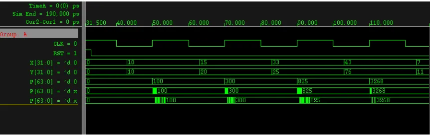
netlist of the design and SDF files for the best-case and worst-case conditions. The post-synthesis simulation of this verilog netlist did not generate any timing violation. The pre-synthesis and post-pre-synthesis output waveforms are shown in Figure 4-1 where X and Y are the 32 bit inputs and P is the 64 bit output. The first P output in Figure 4-1 corresponds to the pre synthesis simulation. The second P output is the post synthesis simulation for the best-case and the third corresponds to the post-synthesis simulation for the worst-case. The delay in the output P for the second and third waveform specifies the actual best-case and worst-case delays of the design.
Figure 4-1: Simulation waveforms for the 32-bit multiplier.
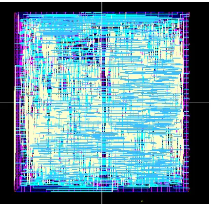
Figure 4-2: Layout of the 32-bit multiplier.
waveforms for the IP forwarding engine specifying the DRAM row and column number is shown in Figure 4-3. The entry in the corresponding row and column of the DRAM specifies the next hop address. Figure 4-4 shows the layout of the IP forwarding engine.
Figure 4-3: Simulation waveform for IP forwarding engine.
Chapter 5 Conclusion and Future Work
The ASIC technology library has been developed for the TSMC 0.25µm standard cell library provided by the VTVT group. The library includes all the basic cells that are needed for synthesis of any design using the Synopsys synthesis tool. All the modifications necessary to incorporate the new TSMC 0.25µm deep submicron technology (provided by the VTVT group) has been made to the NCSU CDK. A tutorial to do placement and routing using Silicon Ensemble has been written for academic use at NC State University. A new Synopsys setup file has been created to link the synthesis tool to the new technology and an example synthesis script has been provided to perform synthesis using Synopsys Design Analyzer.
5.1 Future Work
The cells in the standard cell library were characterized for timing to enable the synthesis tool to check for timing violations in a design. As an extension of this work, the cells can be characterized for the power consumed, modeled for various operating conditions, and modeled for wire loads.
5.1.1 Power
5.1.1.1 Leakage power
Leakage power is the static power dissipated when a gate is not switching. It is important to model leakage power for designs that are in an idle state most of the time. The leakage power information is represented with the cell level
cell_leakage_power attribute and the leakage_power group attribute. The
leakage_power group specifies the leakage power for all the possible steady states of a cell. The cell_leakage_power attribute is the average of all the possible power values for the different states. The power value is in the unit set by the power_unit
attribute. An example of the leakage_power group is shown below where ip1 and ip2 are the inputs of a cell and the value refers to the total leakage power when (ip1, ip2) is (0,0).
leakage_power (){ when: "ip1'*ip2'“; value: 1.1766e-08 }
5.1.1.2 Internal Power
Internal power is the power dissipated within the boundary of the gate. It does not distinguish between the short-circuit power and the switching power.
Short-Circuit Power
Switching Power
Switching power is the power dissipated by the capacitive load on a net whenever the net makes a logical transition. Power is dissipated when the capacitive load at the net is charged or discharged. Switching power along with internal power is used to compute the design’s total dynamic power dissipation.
The CMOS non-linear delay model can be used to describe the power dissipation, in which case the power_lut_template group should be used to create templates of common information that multiple lookup tables can use similar to the
lu_table_template for timing. The table template specifies the table parameters and the breakpoints for each axis. The total power dissipated can be found by giving the output pins a real capacitance, which cause them to be included in the switching power, and modeling only the short-circuit power as the cell's internal power in the
internal_power group. The template variables should be the total output load capacitance and the input transition time similar to the lu_table_template. HSPICE simulations should be run to find the power dissipated for various output loads and input transition times.
5.1.2 Operating Conditions
operating_condition group and a number of groups can be created for various operating conditions. The cell library should be characterized for every new operating condition. Delay scaling factors (k-factors) should then be introduced for each cell to scale the library values defined for nominal operating conditions.
5.1.3 Modeling Wire Load
Bibliography
[1]J.B.Sulistyo and D.S.Ha: Developing standard cells for TSMC 0.25µm technology under MOSIS DEEP rules, Department of Electrical and Computer engineering, Virginia Tech, Technical Report VISC-2002-01, Jan 2002.
[2]Library compiler user guide, volume 1 & 2 v2001.08 Synopsys online documentation [3]Library compiler reference guide, volume 1,2&3 v2001.08 Synopsys online
documentation
[4]Avant! Star HSPICE manual, chapter 27, release 1998.2, Jul 1998
[5]Pronita Mehrotra and Paul D. Franzon: Novel hardware implementation for fast address lookup
Appendix
A1: Inverter worst case library file
/* NCSU TSMC 0.25um Synopsys(TM) library file for worst case. */
library(ncsulib25_worst){
technology (cmos);
delay_model : "table_lookup";
lu_table_template(rise_delay_table) {
variable_1 : total_output_net_capacitance ; variable_2 : input_net_transition ;
index_1("0.0, 20.0, 50.0, 250.0") ;
index_2("34.7291, 146.3404, 368.0077, 872.8222") ; }
lu_table_template(fall_delay_table) {
variable_1 : total_output_net_capacitance ; variable_2 : input_net_transition ;
index_1("0.0, 20.0, 50.0, 250.0") ;
index_2("30.2682, 119.7121, 306.7688, 727.2811") ; }
lu_table_template(rise_delay_table_cd) {
variable_1 : total_output_net_capacitance ; variable_2 : input_net_transition ;
index_1("0.0, 200.0, 1000.0, 5000.0") ;
index_2("35.895, 306.09, 584.445, 1694.23") ; }
lu_table_template(fall_delay_table_cd) {
variable_1 : total_output_net_capacitance ; variable_2 : input_net_transition ;
index_1("0.0, 200.0, 1000.0, 5000.0") ;
index_2("29.453, 258.413, 490.876, 1429.816") ; }
lu_table_template(constraint_table) {
variable_1 : constrained_pin_transition ; variable_2 : related_pin_transition ; index_1("150.0, 600.0, 1200.0") ; index_2("150.0, 600.0, 1200.0") ; }
default_inout_pin_cap : 5.0; default_input_pin_cap : 5.0; default_output_pin_cap : 0.0; default_fanout_load : 1.0;
k_process_wire_cap : 0.0; k_process_wire_res : 1.0; k_temp_pin_cap : 0.0; k_temp_wire_cap : 0.0; k_temp_wire_res : 0.0; k_volt_pin_cap : 0.0; k_volt_wire_cap : 0.0; k_volt_wire_res : 0.0;
input_threshold_pct_fall : 50.0; output_threshold_pct_fall : 50.0; input_threshold_pct_rise : 50.0; output_threshold_pct_rise : 50.0; slew_derate_from_library : 1.00; slew_lower_threshold_pct_fall : 20.0; slew_upper_threshold_pct_fall : 80.0; slew_lower_threshold_pct_rise : 20.0; slew_upper_threshold_pct_rise : 80.0;
time_unit : "1ps"; voltage_unit : "1V"; current_unit : "1mA";
pulling_resistance_unit : "1kohm"; capacitive_load_unit (1.0, "ff");
nom_process : 1.0;
nom_temperature : 125.0;
nom_voltage : 2.25;
cell(inv_1) { area : 41.9904 ; vhdl_name : "inv_1" ;
pin(ip) {
direction : input; capacitance : 4.9614; fanout_load : 1; }
pin(op) {
direction : output; max_capacitance : 250; max_fanout : 50;
function : "ip'";
timing() {
related_pin : "ip";
cell_fall(rise_delay_table) {
values("34.069, 63.316, 58.809, 30.385",\
"109.430, 142.350, 202.760, 209.830",\
"214.060, 254.990, 312.630, 442.820",\
"955.390, 992.520, 1065.800, 1286.200");}
cell_rise(fall_delay_table) {
values("31.295 55.569, 52.091, 84.112",\
"1099.200, 1043.100, 1109.600, 1192.400");}
fall_transition(rise_delay_table) {
values("30.382, 79.778, 138.530, 207.750",\
"129.880, 157.380, 277.980, 365.840",\
"297.480, 310.000, 341.100, 618.780",\
"1510.200, 1486.000, 1410.300, 1480.800");}
rise_transition(fall_delay_table) {
values("37.353, 85.546, 83.193, 210.420",\
"191.480, 166.800, 225.130, 553.980",\
"418.230, 327.740, 377.490, 683.950",\
"1810.500, 1541.000, 1630.700, 1636.200");}
} } } }
A2: Spice file for simulating inverter
* # FILE NAME: /AFS/UNITY.NCSU.EDU/USERS/V/VSUNDAR/CADENCE/SIMULATION/ * inv_1/hspiceS/extracted/netlist/inv_1.c.raw
.PARAM TD=10N PW=10N TRR=5N TRF=5N VDD=2.25 .GLOBAL VDD
.TEMP 125
.SUBCKT INPUT IN OUT
M111 IO IN VDD VDD tsmc25P L=240E-9 W=1.68E-6 AD=1.00799999857432E-12 +AS=1.10880000927377E-12 PD=2.88000001091859E-6 PS=3.00000010611257E-6 M=1
M311 IO IN 0 0 tsmc25N L=240E-9 W=840E-9 AD=503.999999287158E-15 +AS=554.400004636885E-15 PD=2.04000002668181E-6 PS=2.15999989450211E-6 M=1
C55 IN 0 148.06080331468E-18 M=1.0 C75 IN VDD 62.8559989100265E-18 M=1.0 C95 0 IO 296.788803894E-18 M=1.0
C115 VDD IO 165.215999823438E-18 M=1.0
EONE IN2 0 IO 0 1.0
M112 OUT IN2 VDD VDD tsmc25P L=240E-9 W=1.68E-6 AD=1.00799999857432E-12
+AS=1.10880000927377E-12 PD=2.88000001091859E-6 PS=3.00000010611257E-6 M=1
C54 IN2 0 148.06080331468E-18 M=1.0 C74 IN2 VDD 62.8559989100265E-18 M=1.0 C94 0 OUT 296.788803894E-18 M=1.0
C114 VDD OUT 165.215999823438E-18 M=1.0
.ENDS
.SUBCKT INV IP OUT
M1 OUT IP VDD VDD tsmc25P L=240E-9 W=1.68E-6 AD=1.00799999857432E-12 +AS=1.10880000927377E-12 PD=2.88000001091859E-6 PS=3.00000010611257E-6 M=1
M3 OUT IP 0 0 tsmc25N L=240E-9 W=840E-9 AD=503.999999287158E-15 +AS=554.400004636885E-15 PD=2.04000002668181E-6 PS=2.15999989450211E-6 M=1
C5 IP 0 148.06080331468E-18 M=1.0 C7 IP VDD 62.8559989100265E-18 M=1.0 C9 0 OUT 296.788803894E-18 M=1.0
C11 VDD OUT 165.215999823438E-18 M=1.0
.ENDS
.lib "/tsmc025.l" SS .lib "/tsmc025.l" NMOS .lib "/tsmc025.l" PMOS
V0 VDD 0 VDD
VIP1 20 0 PULSE(0, VDD, 0, 2P, 2P, 10N, 20NS) XIP1 20 30 INPUT
CinA 30 0 0fF EA 40 0 30 0 1.0 XAND 40 50 INV CL1 50 0 0fF
.MEASURE in_tran_fall TRIG V(40) VAL="0.8*VDD" FALL=2
+ TARG V(40) VAL="0.2*VDD" FALL=2
.MEASURE in_tran_rise TRIG V(40) VAL="0.2*VDD" RISE=2
+ TARG V(40) VAL="0.8*VDD" RISE=2
.MEASURE cell_fall TRIG V(40) VAL="0.5*VDD" RISE=2 + TARG V(50) VAL="0.5*VDD" FALL=2
.MEASURE cell_rise TRIG V(40) VAL="0.5*VDD" FALL=2
+ TARG V(50) VAL="0.5*VDD" RISE=2
.MEASURE fall_transition TRIG V(50) VAL="0.8*VDD" FALL=2
+ TARG V(50) VAL="0.2*VDD" FALL=2
.MEASURE rise_transition TRIG V(50) VAL="0.2*VDD" RISE=2
+ TARG V(50) VAL="0.8*VDD" RISE=2
********Cin = 0fF******** ********CL = 20fF********
.ALTER
CL1 50 0 20fF CinA 30 0 0fF
********CL = 50fF********
.ALTER
CL1 50 0 50fF CinA 30 0 0fF
********CL = 250fF********
.ALTER
CL1 50 0 250fF CinA 30 0 0fF
********Cin = 20fF******** ********CL = 0fF********
.ALTER
CL1 50 0 0fF CinA 30 0 20fF
********CL = 20fF********
.ALTER
CL1 50 0 20fF CinA 30 0 20fF
********CL = 50fF********
.ALTER
CL1 50 0 50fF CinA 30 0 20fF
********CL = 250fF********
.ALTER
CL1 50 0 250fF CinA 30 0 20fF
********Cin = 50fF******** ********CL = 0fF********
.ALTER
CL1 50 0 0fF CinA 30 0 50fF
********CL = 20fF********
.ALTER
********CL = 50fF********
.ALTER
CL1 50 0 50fF CinA 30 0 50fF
********CL = 250fF********
.ALTER
CL1 50 0 250fF CinA 30 0 50fF
********Cin = 150fF******** ********CL = 0fF********
.ALTER
CL1 50 0 0fF CinA 30 0 150fF
********CL = 20fF********
.ALTER
CL1 50 0 20fF CinA 30 0 150fF
********CL = 50fF********
.ALTER
CL1 50 0 50fF CinA 30 0 150fF
********CL = 250fF********
.ALTER
CL1 50 0 250fF CinA 30 0 150fF
*************************************************** ***************************************************
.OP .save
A3: Synthesis script and synopsys setup file
Example synthesis script
/********************************************************/ /* */ /* Basic NCSU Synthesis Script */ /* Set up for the 0.25u library */ /* */ /* Revision History */ /* 12/15/02: Author S. Vishwanath */ /* */ /********************************************************/ /********************************************************/ /* */ /* Read in Verilog file and map (synthesize) */ /* onto a generic library */ /* */ /********************************************************/
Read -f Verilog mult.v
/********************************************************/ /* */ /* Our first Optimization 'compile' is intended to */ /* produce a design that will meet hold-time */ /* under worst-case conditions: */ /* - slowest process corner */ /* - highest operating temperature and lowest Vcc */ /* - expected worst case clock skew */ /* */ /********************************************************/
/*---*/ /* Specify the worst case (slowest) libraries. */
/* The library has not been characterized */
/* for Operating conditions. */
/*---*/
target_library = {"ncsulib25_worst.db"} link_library = {"ncsulib25_worst.db"}
/*---*/ /* specify a 5000 ps clock period with 50% duty cycle */ /* and a skew of 300 ps */ /*---*/
Create_clock -period 5000 -waveform {0 2500} clock set_clock_skew -uncertainty 300 clock
/* 2. What type of cells are driving the inputs */ /* 3. What type of cells and how many (fanout) must it */ /* be able to drive */ /* */ /********************************************************/
/*---*/ /* ASSUME being driven by a slowest D-flip-flop */ /* The DFF cell has a worst clock-Q delay of 900 ps */ /* Allow another 200 ps for wiring delay */ /* NOTE: THESE ARE INITIAL ASSUMPTIONS ONLY */ /*---*/
set_input_delay 1100 -clock clock all inputs() - clock
/*---*/ /* ASSUME this module is driving a D-flip-flip */ /* The DFF cell has a worst set-up time of 750 ps */ /* Allow another 200 ps for wiring delay */ /* NOTE: THESE ARE INITIAL ASSUMPTIONS ONLY */ /*---*/
set_output_delay 950 -clock clock all_outputs()
/*---*/ /* ASSUME being driven by a D-flip-flop */ /*---*/
set_driving_cell -cell "dp_2" -pin "q" all_inputs() - clock
/*---*/ /* ASSUME the worst case output load is */ /* 3 D-flip-flop (D-inputs) and */ /* and 0.5 units of wiring capacitance */ /*---*/
port_load = 0.5 + 3 * load_of (ncsulib25_worst/dp_2/ip)
set_load port_load all_outputs ()
/********************************************************/ /* */ /* Now set the GOALS for the compile */ /* */ /* In most cases you want minimum area, so set the */ /* goal for maximum area to be 0 */ /* */ /********************************************************/
set_max_area 0
/* DesignWare components. i.e. Make one flat design */ /* 'replace_synthetic' is the cleanest way of doing this*/
/* */
/*---*/
replace_synthetic -ungroup
/*---*/ /* check the design before optimization */ /*---*/
check_design check_timing
/********************************************************/ /* */ /* Now resynthesize the design to meet constraints, */ /* and try to best achieve the goal, and using the */ /* CMOSX parts. In large designs, compile can take */ /* a long time */ /* */ /********************************************************/
/*---*/ /* -map_effort specifies how much optimization effort */ /* there is low, medium, and high */ /* use high to squeeze out those last picoseconds */ /* -verify_effort specifies how much effort to spend */ /* making sure that the input and output designs */ /* are equivalent logically */ /*---*/
compile -map_effort medium -verify -verify_effort medium
/*---*/ /* Now trace the critical (slowest) path and see if */ /* the timing works. */ /* */ /* If the slack is NOT met, you HAVE A PROBLEM and */ /* need to redesign or try some other minimization */ /* tricks that Synopsys can do */ /*---*/
report_timing
/********************************************************/ /* */ /* Now resynthesize the design for the fastest corner */ /* making sure that hold time conditions are met */ /* */ /********************************************************/
target_library = {"ncsulib25_best.db"} link_library = {"ncsulib25_worst.db"} translate
/*---*/ /* Set the design rule to 'fix hold time violations' */ /* Then compile the design again, telling Synopsys to */ /* Only change the design if there are hold time */ /* violations. */ /*---*/
set_fix_hold clock
compile -only_design_rule -incremental
/*---*/ /* Report the fastest path. Make sure the hold */ /* is actually met. */ /*---*/
report_timing -delay min
/*---*/ /* Write out the 'fastest' (minimum) timing file */ /* in Standard Delay Format. We might use this in later*/ /* verification. */ /*---*/
write_timing -output count_min.sdf -format sdf
/*---*/ /* Since Synopsys has to insert logic to meet hold */ /* violations, we might find that we have setup */ /* violations now. SO lets recheck with the slowest */ /* corner etc. */ /* */ /* YOU have problems if the slack is NOT MET */ /* 'translate' means 'translate to new library' */ /*---*/
target_library = {"ncsulib25_worst.db"} link_library = {"ncsulib25_worst.db"} translate
report_timing
/*---*/ /* Write out the resulting netlist in Verliog format */ /*---*/
write -f verilog -o count_final.v
/*---*/ /* Write out the resulting heirarchial netlist */
/* in Verliog format. We will need this */
/* for Silicon Ensemble */
write -hierarchy -format verilog -output count_heirarchy.v
/*---*/ /* Write out the 'slowest' (maximum) timing file */ /* in Standard Delay Format. We might use this in later*/ /* verification. */ /*---*/
write_timing -output count_max.sdf -format sdf
Synopsys setup file: .synopsys_dc.setup designer = "User Name" ;
company = "NCSU " ; /* Search Path variables */
search_path = "/afs/eos.ncsu.edu/dist/cad445/local/TSMC025_deep /afs/eos.ncsu.edu/dist/synopsys35a/packages/IEEE/lib" + search_path
/* Library Variables */
target_library = { ncsulib25_worst.db } link_library = { ncsulib25_worst.db }
symbol_library = { ncsulib25_symbols.sdb basic.sdb } /* IO Port variables */
edifin_lib_in_port_symbol = "ipin" edifin_lib_out_port_symbol = "opin" edifin_lib_inout_port_symbol = "iopin" edifin_lib_in_osc_symbol = "iooff" edifin_lib_out_osc_symbol = "ooff" edifin_lib_inout_osc_symbol = "ioff" edifin_lib_logic_1_symbol = "vdd" edifin_lib_logic_0_symbol = "gnd" edifin_lib_ripper_bus = "bus_end" edifin_lib_route_grid = 1024 edifin_lib_templates=
{{A,landscape,Asize},{A,portrait,Asize.book},{B,landscape,Bsize},{C,landscape,Csize} ,{D,landscape,Dsize},{E,landscape,Esize},{F,landscape,Fsize}}
/* Power and Ground Variables */ edifin_ground_net_name = "gnd!" edifin_ground_net_property_name = "" edifin_ground_net_property_value = "" edifout_ground_name = "gnd"
edifout_ground_net_property_value = "" edifout_ground_pin_name = "gnd!" edifin_power_net_name = "vdd!" edifin_power_net_property_name = "" edifin_power_net_property_value = "" edifout_power_name = "vdd"
edifout_power_net_name = "vdd!" edifout_power_net_property_name = "" edifout_power_net_property_value = "" edifout_power_pin_name = "vdd!"
edifout_power_and_ground_representation = "net" /* Net to Port Connection variables */
edifin_autoconnect_ports = "true" single_group_per_sheet = "true" use_port_name_for_oscs = "false"
write_name_nets_same_as_ports = "true" /* Output variables */
edifout_netlist_only = "false" edifout_target_system = "cadence" edifout_instantiate_ports = "true"
A4: Part of post synthesis library file
The post synthesis library file for an inverter and D-Flipflop is shown below.
/* ************************************************************ */
/* FUNCTION: INV */
/* ************************************************************ */
`celldefine
module inv_1(op, ip);
output op; input ip;
specify
specparam ip_op = 0; (ip=>op)=(ip_op); endspecify
not(op, ip);
/* ************************************************************ */
/* FUNCTION: DFF */
/* ************************************************************ */
`celldefine
module dp_2(q, ck, ip);
output q; input ck, ip;
specify
specparam ck_q = 0; specparam temp = 0;
(ck=>q)= (ck_q);
$setup(edge[01] ip, edge[01] ck, temp); $setup(edge[10] ip, edge[01] ck, temp); $hold(edge[01] ck, ip, temp);
$width(negedge ck, temp); $width(posedge ck, temp);
endspecify
prim_dff U1(q,ck,ip);
endmodule `endcelldefine
/* ************************************************************ */
/* FUNCTION : DFF Primitive table */
/* ************************************************************ */ primitive prim_dff(q,cp,d); output q; reg q; input cp,d; table
/* user defined primitive "prim_dff" as a table --useful for
accelerated simulation and compiling a synthesis library */
// cp d : q : q+
// clocking data on the rising edge
r 1 : ? : 1;
r 0 : ? : 0;
// ignoring the falling edge of the clock
n ? : ? : -;
// ignoring the edges on data
* 0 : 0 : 0;
* 1 : 1 : 1;
? * : ? : -;