A
Planar
Capacitive Micro Positioning Sensor
H i r o a k i c E
Production Engineering Research Laboratory, Hitachi,Ltd.
292 Yoshida-cho,Totsuka-ku,Yokohama 244, Japan
RonaldS. Fearing
Dept. of Electrical Engineering and Computer Sciences, University of California at Berkeley,
Berkeley, CA 94720, USA
Abstrad: A planar capacitive micro positioning sensor has been designed and fabricated for positioning a small
moving object, for example, a micro mobile robot and small parts(under about 5 millimeters). The sensor system consists of a sensor array, formed by driving and sensing electrodes, and a platform(m0ving object) with conductive plates. The principle of detecting position is based on the capacitance change proportional to the platform position. The capacitance between the conductive plate and the sensing electrode varies in proportion to the platform displacement. To detect X,Y positions independently and incrementally, sensing electrodes are divided into four kinds of areas, and to improve the linearity of output signals, the area of driving electrode
is maximized. Using a prototype 30 X 30 mm sensor formed by a printed circuit board, the positioning accuracy is about k 10 micrometers. As for a Si base micro machined 4X 4 mm sensor, the accuracy is estimated within k 3 micrometers. We also made an absolute type sensor array. As these sensor systems enable us to detect positions by simply adding electrode patterns, it will be very useful for micro positioning and assembly.
1. INTRODUCTION
In recent years, small mechanical or electronic components have been miniaturized rapidly. In order
to handle these small parts for assembly and testing purposes, miniature manipulator systems have been researched in the micro electro mechanical system field, for example [1]-[8]. There are many advantages to shrinking robots, actuators and sensors to the same size as the parts to be manipulated. One of the advantages is to "ize the workspace area for manipulator systems. Conventional assembly systems need larger workspace areas in spite of the size of
small parts. Especially the case of workspace in clean rooms, the system size is one of the important factors.
The goal of this research is to develop a micro robot system for assembly and testing. The micro robots can
cooperatively move and manipulate small parts.
Our
&-st research step is to make small and simple sensors
for this purpose.
In many systems, optical sensors, for example TV
cameras for image processing, are often used for
position detection, but the systems need larger space for placing sensors. Considering from the standpoint of system size, capacitive sensing is known to be advantageous and can be used to accurately detect the
presence and position of dielectric and conductive materials[9]. For example, a capacitive incremental position measurement system is used to detect the required position for control two dimensional planar motors on an air bearings[lO][ll]. This system needs individual and complicated sensor patterns for detecting perpendicular directions. Other capacitive planar position sensors have been designedE121. This sensor has predicted resolution of 0.1 pm, but is rather large (18" X 18mm), and requires electrid
connections to the floating platform, which is not possible in our system concept.
A planar capacitive micro positioning sensor is proposed in this paper. The positioning system concept, as shown in Figure 1, mainly consists of a capacitive sensor array for detecting position, a coil array as an actuator for moving objects, a platform as a moving object and an air bearing to reduce fciction between the sensor array and the platform. The capacitive sensor array is designed to be simple to manufacture. It is suitable for fabrication by micro machining technologies and can be miniaturized to less than
millimeter order.
Coil Array for moving Platform
Figure 1. Positioning System Concept
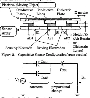
2. PRINCIPLE OF DETECTING POSITION The capacitive micro positioning sensor system consists of a sensor array and a platform as a moving object, as shown in Figure 2. The sensor array is
formed by driving and sensing electrodes on a dielectric plate. Driving and sensing electrodes are arranged at regular intervals. The platform is formed by conductive plates connecting each other electxically with conductive lines on a dielectric plate.
The principle of detecting position is based on the capacitance change proportional to the platform position. The equivalent electrical circuit of this sensor co&guration is shown in Figure 3. The capacitance
(CDip+Cm) between dr;ving electrodes (D1 and DZ) and conductive plates on the platform is almost constant when the platform moves in X direction. Because the total capacitive area (ADl+ADZ) between driving electrodes and conductive plates is constant.
On the other hand the capacitance (Cpsi) between the conductive plate on the platform and the sensing electrode (Sl) varies in proportion to the platform X displacement, because the capacitive area (ASl), which is composed of capacitor between the conductive plate
and the sensing electrode, varies in proportion to the platform X position.
The total capacitance C, between the driving electrodes and the sensing electrode through conductive plates, can be calculated as below:
and the coupling current Isi from the sensor is a
function of the platform position. [Platform moving Object)
I
c
= (CDlF'+ cD2P)CPSl/(CDlP+ CD2P+ CBI)\ Conductive Conductive Dielectric ~
A D 2 (&Bearing
-
orSensing Eledrode Driving Electrodes Dielectric
Laver) Figure 2. Capacitive Sensor Co&guration(cross &&on)
1
constant proportional-
change
-
-
Figure 3. Equivalent Circuit of Sensor
3. INCREMENTAL POSITIONING SENSOR
3.1 X,Y Position Measurement
In
order to detect X,Y positions independently and incrementally, the sensing electrodes are divided into fourkinds
of areas and arranged at regular intervals each other. They are arranged a t other intervals against driving electrodes, as shown in Figure 4.In
this case the platform has 3 X 3 conductive plates connecting each other with conductive lines. When the platform is moving inX
direction above the sensor array, as shown by the dotted lines in Figure 4, the capacitive area between the driving electrodes and the conductive plates is always the same as 1 driving electrode area. On the other hand the capacitive areas between the conductive plates and the sensing electrodes (Sl, S2, S3, S4) are changing like triangular waves. The capacitive area above the sensing electrodes (Sl) is added to another capacitive area above the sensing electrodes (S3) so that the total capacitive area won't become zero according to the platform Y position. Other capacitive areas are also added to other areas, for example, S2+S4, Sl+S2, s3+s4.To calculate the X position and moving direction, the
total capacitive area above (Sl+S3) should be compared
with
the total capacitive area above (SZ+S4). The moving direction inX(+)
orX(-)
direction is detected by the phase difference, the same as in usual incremental encoders. TheX
displacement is a function of the relation between values of a and b, changes of capacitive areas above (Sl+S3) and (S2+S4). In practice the coupling currents are measured as the capacitance changes above (Sl+S3) and (SZ+S4), and the X position can be calculated as a non-linear function of the capacitive areas.At the same time the ratio of the capacitive areas above (Sl+S2) and (S3+S4) should be calculated. If the platform moves only in
X
direction, the ratio should be constant, but if the platform moves in X andY
directions, the ratio wilI be changed and the Y
displacement can be calculated same a s the X
displacement.
3.2 Z Height Measurement
I n the proposed concept positioning system, an air
bearing is used. Compared with the minimum size of the electrode (less than about 100 p), the bearing gap usually should be less than about
low.
A
self-pressurizing squeeze-film air bearing is suitable and the gap is less than about
low.
In the case of small gap(less than l o w ) , the float height Z can be found asa function of the absolute values of measured currents when the platform stops above one point.
Capacitive Area change of Sensing Electmde l(S1) 0 X X Sensing Electrode Z(S2) 0 Sensing Electrode 3(53) Sensing Electmde 4(M)
'
0 X 0 X (Sl+S2) & (S3+S4) 24
Sl+S2 s3+a . Y-
(
m
)
Figure 4. Capacitive Sensor and Capacitive Area Change
3.3 Improvement of Output Signal Linearity
In order to simplify the calculation of the position, the output signal should change linearly. As stated before, the total capacitance C is a fundion of the constant capacitance
CDP,
between the driving electrodes and conductive plates, and the changing capacitance Cps, between the conductive plates and sensing electrodes, as below:C = CDPXCPS/(CDP+ CPS)
If CDP
is large enough, C can be approximately a linearfunction of the CPS. To maximize the capacitive area on
driving electrode, the area of driving electrode can be increased by 5 times as shown in Figure 5.
Compared to the capacitance change with the
capacitive area change, the linearity of the capacitance change w i l l be improved by maximization of driving electrode area as shown in Figure 6.
lectrodes
4
lectrode Xy4
... A . .:..,.. , . . ...- . .Figure 5. Maximization of Driving Electrode Area
-
Capacitive Area Change- . - - - -
Capcitance Change (Driving Electrode Area=l)-
Capcitance Change (Driving Electrode Area=5)0 1 2
X Displacement (relative position)
Figure 6. Capacitive Area Change and Capacitance Change
3.4 Experiments
(1) Prototype Sensor Experiment
To verify the possibility of position detection, Srstly we made and tested a prototype 30x30" sensor formed by a printed circuit board.
The experimental system is schematically shown in Figure 7. The prototype capacitive sensor array is k e d on a plane and the platform is covered with about
5 0 p of plastic tape to give a smooth surface and an
isolation layer instead of using an air bearing. The platform is pushed by a rod connecting to a positioning stage. A sine wave is injected into driving area, the capacitive coupling current (Isi) is measured on one of
4 sensing areas, and the other 3 unaddressed sensing areas are grounded. Using a current to voltage converter and A/D converter, the capacitance change of 0.01-0.001pF can be measured.
\
Capacitive
,
,
,
VO
Driving Area Plastic TapeSensor Array
'0"
Figure 7. Experimental System
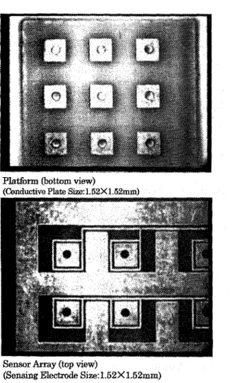
The prototype sensor array and platform is shown
in Figure 8. The size of each conductive plate and
sensing electrode is 1.52 X 1.52 111111. T h e capacitance of prototype sensor is calculated to be on the order of 1pF. The surfaces of conductive plates on the platform and sensor array are not smooth, as shown in Figure 9, and the height diEference is about 2 0 ~ . To eliminate stray capacitance between the driving electrodes and the sensing electrodes on the sensor array, grounded lines are arranged between these electrodes.
Plaffom (bottom view)
K!onductive Plate Shx1.52X1.52mm)
Sensor Array (top view)
(Sensing Electrode SiZe:1.62X1.52mm)
Figure 8. Prototype Sensor h a y and Platform
Sensor Array Through Holes Conductive Plate
100
80
20
0
Figure 9. Roughness of Prototype Sensor Array
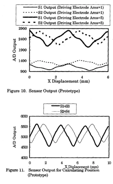
Figure 10 shows the measured relations between the
X
displacement and the 2 kinds of sensor outputsignals. The capacitance changes of output signals from the maximized driving electrode area (=5) are larger than those from driving electrode area (=l), but the output signals have distortion of wave shape between the peak and the valley. This distortion is caused by the through holes on the conductive plates and electrodes. These holes are used for electric connecting lines between other conductive plates and electrodes.
The wave distortion is improved by minimizing these hole effect, and the triangular waves are observed as shown in Figure 11. The output value of capacitance measurement has 10 bits on the A/D converter, about
1000 levels and can be resolved to better than 1%.
The half cycle of platform displacement is 1.52 mm, so
the positioning accuracy is about +1Opm order (.f 1 5 2 0 / ( 1 0 0 - 2 0 0 ) = ~ 1 5 - 8 ~ ) in spite of the rough surface.
S1 Output (Driving Electrode Area=l)
-S2 Output (Driving Electrode Area=l)
S1 Output (Driving Electrode Area=5)
52 Output (Driving Electrode Area=5)
0 2 4 6
X Displacement (mm)
Figure 10. Sensor Output (Protetype)
0 2 4 6 8 10
X Di lacement (mm) Figure 11. Sensor Output for Calc&ting Position
(Prototype)
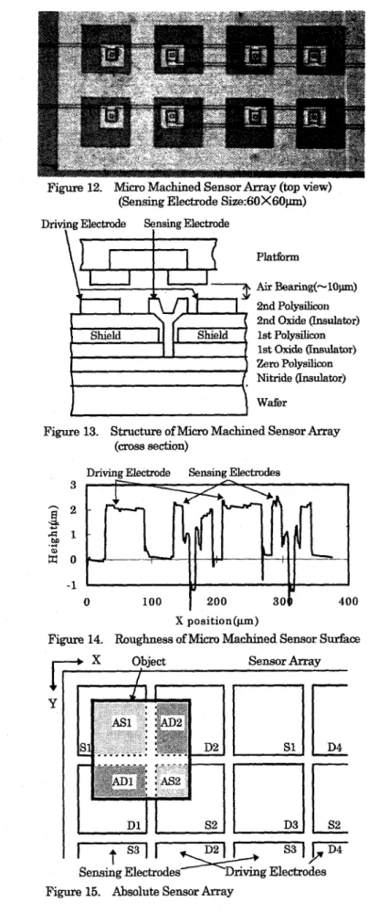
(2)
Micro
Machined Sensor ExperimentAfter the verification of prototype sensor, we made
and
tested a Si base micro machined 4 X 4 mm sensor ,as shown in Figure 12. The
size
of sensing electrodes is 60X60p.m and 25 times as small as the size of the prototype one. The structure of the micro machined sensor array is shown in Figure 13.The thickness of each layers (1-2p1) is very thin
compared with the space between electrodes (15- 4 5 ~ ) . To eliminate stray capacitance, shield layers are arranged between driving electrodes and Zero
polysilicon layer(as an electric connecting line between sensing electrodes). The roughness of sensor array surface is less than 2p.m as shown in Figure 14. The relations between the
X
displacement and sensor output were measured by the same experimental system as before. Instead of using a platform with conductive plates, a dielectric platform without conductive plates was used, because it's diftlcult tocover the platform with a thin dielectric layer. The positioning accuracy is estimated within k3p.m.
4.
ABSOLUTE
POSITIONING SENSORThe incremental sensor is suitable for positioning certain types of objects. For example in the case of moving robots, the size is known and the conductive
plate patterns can be added. As for more general objects, for example small mechanical or electric components, an absolute sensor is preferable in some cases. So an absolute sensor has been made using the similar detecting principle.
The absolute positioning sensor consists of an array formed by driving electrode groups (Y direction) and sensing electrode groups Q direction) running perpendicularly each other, as shown in Figure 15. A sine wave is injected into one of driving electrode groups, and the capacitive coupllng current is measured on one of sensing electrode groups. The array is scanned and the object is detected roughly by the capacitance changes of sensing electrode p u p s .
When the object size is larger than each electrode size, the moving object is dways on multiple electrodes (this case is on 4 electrodes). Capacitive areas (AS, AS2, ADl, AD2) between electrodes on the sensor array and object will be a fundion of object position. To
detect X position precisely, the ratio of the capacitive area (ADl+ASl) and (AD2+AS2) should be compared.
To detect
Y
position, the ratio of (AD2+AS1) and(ADl+AS2) should be compared. This sensor needs many electrode groups depending on the positioning accuracy and sensor size. The possibility of position detection was confirmed by prototype and micro machined sensors.
Figure 12. Micro Machined Sensor Array (top view) (Sensing Electrode Size:GOX60p) D r i T g Electrode Sensing Electrode
i
Zero Polysilimn Nitride (Insulator)
~~
Figure 13. Structure of Micro Machined Sensor Array (cross section)
Drivine Electrode Sensine Electrodes
0 100
I
200 30b 400X position(pm)
Figure 14. Roughness of Micro Machined Sensor Surface
Object Sensor Array
I
Sensing Electrodes
Figure 15. Absolute Sensor Array
5. CONCLUSION AND FUTURE WORX This paper has shown the possibility of using planar capacitive micro positioning sensors €or detecting a
small object. According to the experiment results, the positioning accuracy
can
be obtained almost 1/20-1/100 of electrode size. With better characterization of the sensitivity of coupling currents and the roughness of the surface, it should be possible to improve the
positioning accuracy.
The main points of designing sensor are as follows:
1. detecting method (incremental or absolute)
2. sensor size and positioning accuracy
3. sensor signal characteristic (sensitivity, linearity and stray capacitance).
Our
further research is to optimize the sensor patterns for detecting plural objects and rotational motion. Furthermore, it‘s necessary to combine the sensor with actuator systems.References
[I] K. Pister, R. Fearing and R. Howe, “A planar air levitated eledrostatic actuator system”, IEEE Micro Electro Mechanical Systems, Napa Valley, CA, pp.67-71, Feb.1990.
[2] R. Fearing, “A miniature mobile platform on an air
bearinf, 3rd Int. Symp. on Micromachine and Human Science, Nagoya, Japan, pp.111-127, Oct. 1992.
[3] S. Konishi and H. Fujita, “A conveyance system using air flow based on the concept of distributed micro motion systems”, Int. Conf on Solid-state Sensors and Actuators, Yokohama, Japan, pp.28-31, June 1993.
[4] M. Ataka, A. Omodaka, N. Takeshima, and H. Fujita, “Fabrication and Operation of a Polyimide Bimorph Actuators for a C h r y Motion System,” Jnl. of Micro electro mechanical Systems, vo1.2,no.4, pp.146-150, Dec. 1993. [5] K. Boehringer, B. Donald, R. Milhailovich, N. MacDonald, “Sensorless Manipulation Using Massively Parallel Mimhbricated Actuator Arrays”, IEEE Int. Conf. on Robotics and Automation, San Diego, CA, pp.826-833, May 1994. [6] R. Fearing, “A Planar Milli-Robot System on an
Air
Bearing”, 7th Int. Symp. on Robotics Research, Herrsching, Germany, Oct. 1995.
T. Inoue, K Iwatani, I. Shimoyama and H. Miura, ‘Wimmanipulation Using Magnetic Field”,
IEEE
Int. C o d on Robotics and Automation,Nagoya, Japan,pp.679-684,May 1995 [SI W. Liu and P. Will, ”Parts Manipulation on an Intellgent Motion Surface“, Proc. IEEE-RSJ Intelligent Robots and Systems, Pittsburgh, PA, pp.399-404, Aug. 1995.[9] K Klaassen and J. Van Feppen, “Linear Capacitive
Microdisplacement transduction using phase read out”, Sensors and Actuators, vol. 3, pp.209-220, 1983.
[lo]
G.Miller,“Capacitive incremental position measurement and motion control”, United States Patent 4893071, Jan.1990. [ll] G. Miller, “Capacitively commutated brusbless DCservomotors”, United States Patent 495811, Sep. 1990. [12] M. Bonse, F. Zhu, and J. Spronck, “A New Two
Dimensional Capacitive Position Transducer”, Sensors and Actuators, vol. 41-42, pp.29-32, 1994.